الشبكة الفائقة الجرافينية النانوية المسامية الوظيفية Functional nanoporous graphene superlattice

المجلة: Nature Communications، المجلد: 15، العدد: 1
DOI: https://doi.org/10.1038/s41467-024-45503-9
PMID: https://pubmed.ncbi.nlm.nih.gov/38346953
تاريخ النشر: 2024-02-12

الشبكة الفائقة الجرافينية النانوية المسامية الوظيفية

تاريخ الاستلام: 19 يوليو 2023
تم القبول: 26 يناير 2024
نُشر على الإنترنت: 12 فبراير 2024
(ت) تحقق من التحديثات

هوليانغ لو يوشينغ ياو © مينغ يوي يوان غوانيو تشين يوتشاو وانغ لونغجون راو شوقونغ أوفوما I. كارا روبرت ل. دوبونت تشنغ زانغ بويوان تشين بو ليو شياودي زو رينبينغ وو سليمان أدييرا رينتشاو تشي شينغتساي تشانغ شياوجوانغ وانغ

الملخص

لقد ظهرت السوبرلاتيس ثنائية الأبعاد (2D)، التي تتكون من تكديس تحت الشبكات لمواد ثنائية الأبعاد، كمنصة قوية لتعديل وتعزيز خصائص المواد بما يتجاوز خصائصها الجوهرية. ومع ذلك، فإن طرق التخليق التقليدية محدودة بالشبكات الفرعية لمواد ثنائية الأبعاد النقية، مما يشكل تحديًا عمليًا كبيرًا عندما يتعلق الأمر بتكديس الشبكات الفرعية المعدلة كيميائيًا. هنا، نبلغ عن طريقة تخليق كيميائية تتغلب على هذا التحدي من خلال إنشاء سوبرلاتيس جرافين ثنائية الأبعاد فريدة، حيث يتم تكديس الشبكات الفرعية للجرافين مع مسام مربعة الشكل بحجم نانومتر وحيدة التوزيع وعناصر مشوبة بشكل استراتيجي عند حواف المسام. تظهر السوبرلاتيس الناتجة من الجرافين ارتباطات ملحوظة بين الأطوار الكمومية على كل من مستويات الإلكترون والفونون، مما يؤدي إلى وظائف متنوعة، مثل درع الكهرومغناطيسية، وجمع الطاقة، والإلكترونيات الضوئية، والإلكترونيات الحرارية. بشكل عام، لا توفر نتائجنا فقط مبادئ التصميم الكيميائي لتخليق وفهم السوبرلاتيس ثنائية الأبعاد الوظيفية، بل توسع أيضًا من وظيفتها المعززة وإمكانات تطبيقها الواسعة مقارنة بنظيراتها النقية.

لقد ظهرت الهياكل الفائقة ثنائية الأبعاد (2D)، المكونة من طبقات فرعية مكدسة من المواد ثنائية الأبعاد، كمنصة قوية لتصميم مواد ذات خصائص فريدة ومخصصة غير موجودة في المواد الأصلية. تؤدي التباينات الهيكلية والتركيبية في السوبرلاتيس ثنائي الأبعاد إلى ظواهر إلكترونية وفونونية مرتبطة بقوة، تشمل مراحل كمومية متنوعة. مثال بارز هو السوبرلattice موير الغرافين، الذي تم تحقيقه من خلال تكديس طبقات الغرافين مع التحكم الدقيق في زوايا الالتواء أو الشبكة.
درجات عدم المحاذاة ، مما يؤدي إلى ظواهر مثل انتقال المعدن-العازل، والمغناطيسية الحديدية، وتأثير هول الكمي الشاذ، والنيماتية، وحالات بلورة ويجنر القابلة للتعديل والعزل موت تتركز الأبحاث الحالية حول الهياكل الفائقة ثنائية الأبعاد بشكل أساسي على نمو وتكديس الشبكات الفرعية للمواد ثنائية الأبعاد النقية، من خلال تكديس شبكات فرعية مختلفة بشكل دوري أو من خلال تكديس غير متماسك لشبكات فرعية متطابقة، باستخدام تقنيات مثل ترسيب الشعاع الجزيئي، ترسيب البخار الكيميائي، أو ترسيب الطبقات الذرية. . ومع ذلك، فإن تخليق
تقدم الهياكل الفائقة ثنائية الأبعاد المكونة من شبكات فرعية لمواد ثنائية الأبعاد معدلة كيميائيًا، مثل تلك التي تحتوي على فراغات أو مسام دورية، تحديًا كبيرًا. . بشكل خاص، استكشاف هياكل السوبرلاتس ثنائية الأبعاد في الجرافين المسامي النانوي، وهو عضو بارز من المواد ثنائية الأبعاد المعدلة كيميائيًا ذات الوظائف الفريدة والتطبيقات المحتملة لا يزال غير مستكشف إلى حد كبير.
في هذه الدراسة، نقدم نهجًا كيميائيًا لتصنيع مجموعة من هياكل السوبرلاتيس ثنائية الأبعاد من خلال تكديس الجرافين مع مسام مربعة الشكل بحجم نانومتر وحيدة التوزيع كطبقات فرعية لإدخال درجات حرية إضافية لتشكيل الهيكل الإلكتروني وهيكل الفونون للسوبرلاتيس. من خلال استخدام النمو في الموقع وحفر جزيئات أكسيد المعادن ذات الشكل المكعب على سطح الجرافين، نحقق كثافة عالية من المسام النانوية المربعة وحيدة التوزيع. كما يتم توليد دورية تركيبية من خلال إضافة عناصر محددة إلى حواف المسام بشكل انتقائي. تشير التحليلات النظرية إلى أن هيكل السوبرلاتيس ثنائي الأبعاد يحفز إعادة بناء الهياكل الإلكترونية والفونونية للجرافين، مما يؤدي إلى تسطيح نطاق الطاقة الإلكترونية، وظهور فجوة في نطاق الفونون، وزيادة كبيرة في اقتران الإلكترون والفونون. نتيجة لذلك، يظهر السوبرلاتيس الجرافيني خصائص فريدة، مثل الاسترخاء العازل عند الترددات المنخفضة، وانخفاض الموصلية الحرارية، وانخفاض الانبعاثية تحت الحمراء، وزيادة تأثير سيبيك، وتأثير الفوتولومينسنس، مما يجعله مادة جذابة لمجموعة متنوعة من التطبيقات بما في ذلك تعديل الموجات الكهرومغناطيسية، وجمع الطاقة، وإدارة الحرارة، والإلكترونيات الضوئية، والإلكترونيات الحرارية. تقدم استراتيجيات التخليق المعروضة في هذه الدراسة أساسًا لتطوير
الطبقات الفائقة من خلال تكديس المواد ثنائية الأبعاد المسامية، مما يمهد الطريق لتصميم طبقات فائقة ثنائية الأبعاد بخصائص قابلة للتعديل ووظائف غير مسبوقة مقارنةً بنظيراتها النقية.

النتائج

تركيب سوبرلاتيس الجرافين المسامي

قمنا بإنشاء شبكات فرعية من الجرافين من خلال إنشاء كثافة عالية من المسام النانوية ذات الشكل المربع والمتجانسة في الحجم على الجرافين. تتضمن العملية ثلاث خطوات، كما هو موضح في الشكل 1a: (i) النمو في الموقع لجزيئات نانوية من أكسيد الحديد المكعب. ) قالب على أسطح الجرافين (الشكل التكميلي 1)؛ (ii) حفر في الموقع لذرات الكربون من خلال تفاعل الاختزال بين الجرافين و الجزيئات النانوية؛ و (iii) إزالة قوالب الجسيمات النانوية بواسطة حمض الهيدروكلوريك. أكدت حيود الأشعة السينية (XRD) تطور الطور للكربون عند الاختزال (الشكل التكميلي 2). توضح الصور الميكروسكوبية الإلكترونية الناقلة التمثيلية في الشكل 1ب الجرافين أحادي الطبقة الناتج الذي يمتلك مسام مربعة متجانسة بحجم متوسط من نفس حجم المكعب جزيئات نانوية.
قمنا بتوسيع طريقتنا لتكديس الشبكات الفرعية للجرافين لإدخال نانوثقوب على الجرافين ثنائي الطبقة، حيث تتداخل الثقوب في طبقة واحدة جزئيًا مع تلك الموجودة في الطبقة الأخرى (الشكل 1c-e). تُعزى الثقوب المتداخلة جزئيًا إلى وجود جزيئات أحادية التوزيع غير المتراصة. جزيئات النانو في كل من الطبقات العليا والسفلى. إن تكديس هذين الشبكتين المسامتين من الجرافين بشكل غير متناسق يخلق ترتيبًا مميزًا لذرات الكربون مع دورية تبلغ

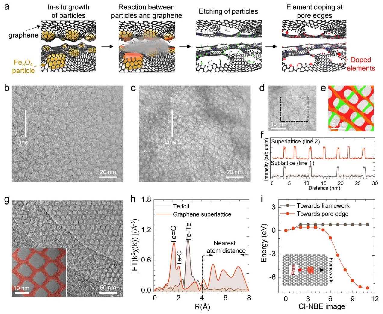
سوبرلattice الجرافين. تمثيل تخطيطي لعملية تخليق سوبرلattice الجرافين. تتضمن العملية لإنشاء سوبرلattice الجرافين المدعوم بالعناصر زراعة جزيئات أكسيد الحديد على الجرافين، تليها حفر الكربون، وإزالة الجزيئات النانوية باستخدام حمض الهيدروكلوريك، وتدعيم العناصر في سوبرلattice الجرافين. صور مجهرية إلكترونية ناقلة تظهر (ب) سوبرلattice الجرافين أحادي الطبقة مع مسام نانوية مربعة الشكل متجانسة الحجم و(ج-هـ) سوبرلattice الجرافين ثنائي الطبقة مع مسام نانوية مربعة الشكل متداخلة جزئيًا. الطبقات العليا والسفلى في سوبرلattice الجرافين في (هـ) هي
متميز بالأحمر والأخضر، على التوالي. الترتيب الدوري لذرات الكربون في (ب) شبكة أحادية الطبقة من الجرافين و (ج) شبكة ثنائية الطبقات من الجرافين. (ز) صورة مجهر إلكتروني ناقل تمثل الجرافين مع مسام مربعة متداخلة. الصورة المصغرة في (ز) تقدم صورة مجهر إلكتروني ناقل مكبرة للجرافين. طيف الامتصاص الممتد للأشعة السينية (EXAFS) الملائم لرقائق التيلوريوم ورقائق الجرافين المدعومة بالتيلوريوم. i حسابات نظرية الوظائف الكثيفة (DFT) لطاقة الانتشار لذرات التيلوريوم المدعومة نحو حافة المسام أو الإطار. الصورة المصغرة في (i) توضح مسار الانتشار الذري للعنصر المدعوم على سطح الجرافين.
(الشكل 1f). لفحص تأثير تكديس الشبكات الفرعية غير المتراصة، قمنا بتخليق الجرافين مع مسام نانوية متداخلة تمامًا (الشكل 1g). تعتبر المسطحات العالية للجرافين، ومجموعة كثيفة من الهياكل النانوية ذات الحجم المتجانس، ومدة تفاعل تقليل الكربون المثلى ضرورية لإنشاء مسام نانوية مرتبة. يُعزى التشوه أو التوزيع المتعدد في المسام النانوية إلى الظروف غير المثلى أو القوالب غير المنتظمة (الأشكال التكميلية 3 و4). هنا نشير إلى الجرافين ثنائي الطبقة مع مسام مربعة متداخلة جزئيًا باسم الجرافين السوبرلattice.
لتحقيق تباين تركيبي، نقوم بضبط نوع المجموعات الوظيفية بدقة عند حواف المسام من خلال إضافة العناصر. كانت حواف المسام في السوبرلattice الجرافيني الذي تم الحصول عليه تحتوي على روابط غير متحكم فيها بين الكربون (C) والأكسجين (O)، بما في ذلك -CO- و-COOH، كما تم تحديده بواسطة مطيافية الأشعة تحت الحمراء بتحويل فورييه (FT-IR) ومطيافية طاقة الإلكترون بالأشعة السينية (XPS) ورسم خرائط العناصر باستخدام المجهر الإلكتروني الناقل (TEM) (الشكل التكميلي 5). لتحضير الجرافين المسامي المدعوم بالهيدروجين (H) والمدعوم بالأكسجين (O)، قمنا بتسخين الجرافين في وجود جو من غاز الهيدروجين عند و ، على التوالي، لتحويل جميع الروابط الحافة إلى و روابط (الشكل التكميلي 6). تم تحقيق إضافة عناصر متعددة، بما في ذلك التيلوريوم (Te) والسيلينيوم (Se) والنيتروجين (N) والفوسفور (P) والكبريت (S) والبورون (B)، من خلال معالجة حرارية ثانوية لاستبدال روابط -C-H عند حواف المسام في الجرافين المسامي المدعوم بالهيدروجين.
استخدمنا السوبرلattice الجرافيني المدعوم بالتيلوريوم كمثال لتحليل حالة وتوزيع العناصر المدعومة على أسطح الجرافين. أظهر تحليل هيكل الامتصاص الممتد للأشعة السينية (EXAFS) (الشكل 1h والشكل التكميلي 7) نوعين من روابط التيلوريوم الموجودة عند حواف المسام بطول و ، بما يتماشى مع حسابات نظرية الكثافة الوظيفية (DFT) (الشكل التكميلي 8). يشير ظهور قمم متتالية تتراوح من
إلى ، بما يتجاوز الطول النموذجي للروابط التساهمية أو الأيونية، إلى تكوين روابط تيلوريوم معلقة عند حواف المسام. كشفت حسابات DFT باستخدام طريقة الحزام المرن المدفوع بالصورة المتسلقة أن انتشار ذرات التيلوريوم نحو حافة المسام له حاجز طاقة أقل (0.42 eV) ورابطة أقوى (-7.41 eV) مقارنة بالانتشار نحو الإطار، مما يشير إلى تفضيل إضافة العناصر عند حواف المسام (الشكل 1i، الشكل التكميلي 9 والملاحظة 1).

الهيكل الإلكتروني والصوتي للسوبرلattice الجرافيني

استخدمنا حسابات DFT لمقارنة الهياكل الإلكترونية للجرافين الثنائي الطبقة النقي مع السوبرلattice الجرافيني. يوضح الشكل 2a أن السوبرلattice الجرافيني يظهر تسطيحًا ملحوظًا للشرائط بالقرب من مستوى فيرمي، يتميز بتشتت شرائط ضئيل (أقل من 1 ميلي إلكترون فولت). ينشأ هذا الهيكل ذو الشرائط المسطحة من العلاقة الضعيفة لتشتت الطاقة الحركية الناتجة عن إعادة بناء إلكترونية دورية ناتجة عن الضغط الذري بين المناطق الكربونية المتداخلة والمكشوفة، مما يؤدي إلى ظهور قمة انتقال جديدة في امتصاص الأشعة السينية لحافة C K (الشكل التكميلي 10 والملاحظة 2). تؤدي هذه إعادة البناء الإلكترونية إلى تكوين جدران مجال الإلكترون التي تحصر إلكترونات فيرمي على كلا الجانبين، مما يؤدي إلى سطح فيرمي متساوي الجهد وحواجز طاقة مع الأسطح المجاورة . يؤدي تأثير احتجاز الإلكترون إلى قرب أكبر من الإلكترونات التكافؤية في السوبرلattice الجرافيني إلى مستوى فيرمي، مما يؤدي إلى تكوين العديد من التفردات في فان هوف ، كما يتضح من توزيع كثافة الحالة الإلكترونية في الشكل 2b.
تؤدي المواد المدعومة في السوبرlattice الجرافيني إلى زيادة كثافة الحالة الإلكترونية على كلا الجانبين من مستوى فيرمي، وزيادة ملحوظة في تفاعل الإلكترون-إلكترون، وزيادة في اقتران الدوران-المدار ، مما يؤدي إلى ضعف العلاقة بين الإلكترونات والطاقة الحركية، مما ينتج عنه نظام إلكتروني مع
الشكل 2 | حساب نظرية الكثافة الوظيفية (DFT) للهيكل الإلكتروني والصوتي للسوبرlattice الجرافيني. أ هيكل الشريط وكثافة الحالة المتوقعة للجرافين النقي والسوبرlattice الجرافيني. يمثل مستوى فيرمي. تشير الأسهم في (أ) إلى التفردات في فان هوف. ب فرق كثافة الشحنة بين ذرات الكربون المتداخلة والمكشوفة في السوبرlattice الجرافيني.
ج-هـ كثافة الحالة الصوتية، هيكل شريط الصوت، وسرعة مجموعة الصوت للسوبرlattice الجرافيني. تم تعيين نسبة تداخل المسام في السوبرlattice الجرافيني، المحددة بنسبة مساحة المسام المغطاة بواسطة طبقة جرافين مجاورة إلى إجمالي مساحة المسام، إلى 0.5. تم إضافة التيلوريوم إلى السوبرlattice الجرافيني. تمثل المناطق المظللة باللون الأخضر، المشار إليها بالأسهم في (د)، فجوة شريط الصوت.
كتلة لانهائية وزيادة في تفاعل كولوم بين الإلكترونات، مما يساهم في تسطيح الشريط المعزز. تدعم هذه التحليلات الحسابية قياسات تركيز حامل هول، مما يكشف عن زيادة تقريبية بنسبة في تركيز الحامل وانخفاض كبير بنسبة 99.8% في حركة الحامل في السوبرlattice الجرافيني مقارنة بالجرافين النقي (الشكل التكميلي 11). تكشف الدراسة الحسابية أن تسطيح الشريط الإلكتروني يتأثر بعوامل مختلفة، مثل الدورية الهيكلية، وأنواع ونسب المواد المدعومة، وأشكال المسام (الأشكال التكملية 12-16 والملاحظة 3). يفتقر الجرافين الثنائي الطبقة مع مسام دائرية متداخلة جزئيًا أو مسام مربعة متداخلة تمامًا إلى هيكل شريط مسطح بسبب غياب مجال إلكتروني دوري محدد جيدًا، مما يعزى إلى الضغط الكبير بين ذرات الكربون المكشوفة والمتداخلة، مما يعطل تكوين جدران مجال الإلكترون في هذه الهياكل الجرافينية.
درسنا تأثير هيكل السوبرlattice على هيكل الصوت في الجرافين. بسبب الاهتزاز التوافقي لشبكة الذرات ، يظهر الجرافين النقي بشكل أساسي أصوات ذرات مع تردد 50 تيراهيرتز (الشكل 2c). على النقيض من ذلك، فإن التداخل الدوري لذرات الكربون في السوبرlattice الجرافيني الثنائي الطبقة يثبط الاهتزازات التوافقية، مما يؤدي إلى أنماط صوتية مميزة في المناطق المتداخلة والمكشوفة. تمتلك المواد المدعومة عند حواف المسام نفس أنماط الاهتزاز الصوتي التي يمكن أن تؤدي إلى تجمعات من أصوات جديدة ، كما يتضح من كثافة الاهتزاز للحالات (الشكل التكميلي 17 والملاحظة 4). يظهر انتقال تجمعات الصوت في السوبرlattice الجرافيني تداخلًا متماسكًا كبيرًا وتشتتًا مرنًا ، مما يؤدي إلى ضعف طاقة تجمعات الصوت وظهور سلسلة من الموجات الثابتة المستمرة في النطاق الترددي المنخفض من ، بينما تختفي الأصوات عالية التردد الأصلية.
إن غياب الأصوات عالية التردد يؤدي إلى انكماش حجم المنطقة الأولى من بريلوان، مما يسبب طي وضغط فروع الصوت الصوتية ويؤدي إلى فجوات شريط الصوت في النطاق الترددي العالي ، مقارنة بالجرافين النقي (الشكل 2d والشكل التكميلي 18). تشير الحسابات إلى أن نسب المشاركة الذرية في السوبرlattice الجرافيني هي أقل من تلك الخاصة بالجرافين النقي (الشكل التكميلي 19)، مما يؤكد أن انخفاض نسبة الذرات المشاركة في نفس النمط الصوتي يؤدي مباشرة إلى تقليل طاقة الصوت وسرعات التجمعات (الشكل 2e). تؤدي النتيجة المتمثلة في توطين الأصوات وتأثير احتجاز الإلكترون إلى اقتران قوي بين الإلكترون والصوت، حيث تمتص الإلكترونات الأصوات، وتخضع للحركة، وتشتت لإثارة أصوات جديدة . تعطي هذه الدورة المستمرة تأثير سحب صوتي بارز، مما يؤثر بشكل كبير على المسارات وخصائص نقل الإلكترونات في السوبرlattice الجرافيني . باختصار، يظهر السوبرlattice الجرافيني ارتباطات كمية ملحوظة على كلا المستويين الإلكتروني والصوتي، مما يؤدي إلى مجموعة متنوعة من الوظائف التي تتجاوز تلك التي لوحظت في الجرافين النقي. تمهد استراتيجيات التخليق لدينا الطريق لتصميم المواد ثنائية الأبعاد ، وخاصة السوبرlattices ثنائية الأبعاد ذات الخصائص القابلة للتعديل والوظائف غير المسبوقة مقارنة بالنظائر النقية.

تعديل الموجات الكهرومغناطيسية للسوبرlattice الجرافيني

أثارت التقدمات المتزايدة في الاتصالات اللاسلكية، وخاصة الجيل الخامس من شبكة الهاتف المحمول (5G)، مخاوف بشأن عدم الاستفادة الكافية من الموجات الكهرومغناطيسية والتداخل المزعج للإشارات تتمتع المواد الكهرومغناطيسية الحالية بحدود في فعاليتها، خاصة مع السماكات التي تصل إلى عشرات الميكرومترات. نحن نبحث في السوبرلاتيسات من الجرافين لتنظيم الموجات الكهرومغناطيسية بكفاءة واستغلال الطاقة الكهرومغناطيسية المكانية. توضح الشكل 3أ والشكل التكميلي 20 سلوك تشتت عازل ملحوظ في الترددات المنخفضة. المنطقة، التي تتوافق مع نطاق الاتصالات اللاسلكية الحالي، الملاحظة في السوبرلاتيس الجرافيني المدعوم بالعناصر. تنشأ هذه التشتت العازل المميز من إعادة تكوين إلكترونية ناتجة عن الضغط الذري عند التقاطعات.
من كل من المناطق الكربونية المتداخلة والمكشوفة. يبدأ هذا إعادة التكوين بإنشاء جدران مجال الإلكترون، مما يؤدي إلى احتجاز إلكترونات فيرمي على كلا الجانبين وتوليد فرق جهد بين السطوح المجاورة. عند تعرضها لحقول كهرومغناطيسية معدلة، يعيد هذا الجهد توجيهه ديناميكيًا استجابةً للمجال الكهربائي المعدل، مما يؤدي إلى سلوك استرخاء الاستقطاب. يتميز هذا السلوك الاسترخائي بانخفاض حاد في السماحية الحقيقية ( ) وقمة رنين العازل في السماحية التخيلية ( )، مما أدى إلى زيادة كبيرة في امتصاص الموجات الكهرومغناطيسية، مما يساهم في تبديد الموجات الكهرومغناطيسية كحرارة جول وتقليل انعكاس الموجات الكهرومغناطيسية والتداخل الثانوي. نُنسب ذلك إلى استرخاء الاستقطاب العازل، كما يتضح من منحنى كول-كول (الشكل التكميلي 21 والملاحظة 5)، الذي ينشأ من جدران المجال الإلكتروني الدورية. .
هذا السلوك التشتتي يؤدي إلى كفاءة امتصاص لشبكة الجرافين الفائقة في المنطقة، ضمن نطاق السماكة ، التي تتجاوز تلك الخاصة بالجرافين النقي بمقدار مرتين (الشكل 3ب). حتى عند سمك يبلغ فقط يمكن أن يتجاوز الامتصاص نظرًا لارتفاع معامل امتصاص الموجات الكهرومغناطيسية، يمكن أن تصل فعالية الحماية الكهرومغناطيسية المتوسطة لطبقات الجرافين الفائقة إلى 99.99% (مما يتوافق مع فعالية الحماية الكهرومغناطيسية )، مما يعالج بشكل فعال التداخل الكهرومغناطيسي الناتج عن الانعكاس الثانوي. تتجاوز قدرات امتصاص الكهرومغناطيسية لشبكة الجرافين الفائقة في نطاق سمك الميكرومتر تلك الخاصة بجميع المواد الكهرومغناطيسية الموجودة (الجدول التكميلي 1). أظهر المقارنة المباشرة لقدرة الحماية الكهرومغناطيسية أن فعالية الحماية الكهرومغناطيسية وكفاءة امتصاص الكهرومغناطيسية لكل سمك مادة لشبكة الجرافين الفائقة كانت أعلى بمقدار من مرتبتين إلى أربع مراتب من المواد ثنائية الأبعاد التقليدية، بما في ذلك MXene وغيرها من الجرافين المعدل كيميائيًا، كما هو موضح في الشكل 3c. لقد أظهرنا القدرة على ضبط كفاءة امتصاص الكهرومغناطيسية من خلال تعديل كميات العناصر المشوبة وتحويل تردد الامتصاص الكهرومغناطيسي الأقصى من خلال اختيار نوع العنصر المشوب (الشكل التكميلي 22). تمتص هذه الشبكة الفائقة من الجرافين الموجات الكهرومغناطيسية بشكل انتقائي عند طول موجي محدد بينما تسمح بانتقال نطاقات أخرى، مما يقلل من فقدان الإشارة ويقدم إمكانية التكامل في الدوائر المصغرة لامتصاص كهرومغناطيسي فعال.
إن إعادة بناء الإلكترون التي triggered بواسطة المجال الإلكتروني لا تؤثر فقط على امتصاص EM ولكنها تقلل أيضًا بشكل ملحوظ من النفاذية المعقدة النسبية. ). هذا التخفيض يحسن بشكل كبير من مطابقة المقاومة، مما يسمح لموجات الكهرومغناطيسية الواردة باختراق المادة بشكل أكثر فعالية، على عكس السلوك السطحي المعتاد الذي يُلاحظ مع الجرافين النقي. وفقًا لمبادئ تصميم الهوائيات، يعمل فيلم السوبرلاتيس الجرافيني لدينا كهوائي، محولًا الموجات الواردة إلى تيارات ومولدًا ناتجًا كهربائيًا كبيرًا. توضح الشكل 3d، جنبًا إلى جنب مع الأشكال التكميلية 23 و24 والملاحظة 6، بشكل أنيق تصميم وعملية تصنيع جهاز السوبرلاتيس الجرافيني. كما هو موضح في الشكل 3e، فإن الجهد المفتوح المقاس ( ) من السوبرلattice الجرافين زادت من 0.1 فولت إلى 6.4 فولت مع زيادة في قوة انبعاث الموجات الكهرومغناطيسية من 1 مللي واط إلى 10 واط، على التوالي. أظهر الجهاز القائم على السوبرلattice الجرافين أقصى قدرة إنتاجية تبلغ 0.31 واط مع مقاومة تحميل قدرها عند التعرض لمصدر طاقة بقوة 10 واط (الشكل التوضيحي 25)، وإنتاج كهرباء مستقر حتى بعد 1000 دورة انحناء أو في حالات انحناء مختلفة (الشكل التوضيحي 26). علاوة على ذلك، تم حساب الكفاءة العامة لتحويل EM-DC لتكون عند قدرة انبعاث EM تبلغ 100 مللي واط، كما هو موضح في الشكل 3f. من الجدير بالذكر أن جهازنا كان قادرًا على جمع وتحويل موجات EM من هاتف خلوى 5G، وجهاز توجيه الواي فاي، وبرج الاتصالات، وميكروويف إلى كهرباء تيار مستمر يمكن استخدامها لتشغيل الأجهزة الإلكترونية مثل الصمامات الثنائية الباعثة للضوء (LEDs) ومقاييس الرطوبة والحرارة الرقمية، كما هو موضح في الشكل 3g والأفلام التكميلية 1-4.

تطبيقات موسعة لشبكة الجرافين الفائقة

بالإضافة إلى تعديل EM، تكشف السوبرلاتيسات من الجرافين عن خصائص إلكترونية وفونونية فريدة، مما يشير إلى تطبيقات محتملة في
الشكل 3 | السماحية وتعديل الموجات الكهرومغناطيسية للجرافين
شبكة فائقة. سماحية تعتمد على التردد لشبكة الجرافين الفائقة. و تمثل الجزء الحقيقي والجزء التخيلي من النفاذية، على التوالي. الخط العمودي المتقطع يحدد التردد الذي يتوافق مع ذروة فقدان العزل.
b كفاءة امتصاص الموجات الكهرومغناطيسية (EM) المعتمدة على السمك لثنائي طبقات الجرافين النقي وسوبرلاتيس الجرافين. تمثل أشرطة الخطأ الانحرافات المعيارية من ثلاث قياسات مستقلة على نفس العينات الفيزيائية. ج مقارنة فعالية درع EM ( وكفاءة امتصاص EM ) متوسط بسمك مادة امتصاص EM من السوبرلattice الجرافين مع أنابيب الكربون النانوية (CNTs) ومواد ثنائية الأبعاد (2D) أخرى. النقاط البيانية المقارنة في (c) مأخوذة من المراجع التكميلية 82-96. d إعداد تجريبي لمحول الكهرباء EM القائم على السوبرلattice الجرافيني. e دائرة مفتوحة
جهد كهربائي ( ) و تحويل EM-electivity للغرافيت النقي ومحول EM-electricity القائم على السوبرلاتيس الغرافيتي كدالة لقوة انبعاث EM. يتم تعريف كفاءة تحويل EM إلى كهرباء كنسبة القدرة الناتجة عن جهاز الغرافيت، الذي يحول الطاقة EM المدخلة إلى تيار مستمر، إلى قوة EM المدخلة. تمثل أشرطة الخطأ الانحرافات المعيارية من ثلاث قياسات مستقلة على نفس العينات الفيزيائية. صور فوتوغرافية لتحويل EM-electricity بواسطة محول EM-electricity القائم على السوبرلاتيس الغرافيتي من هاتف خلوى 5G، جهاز توجيه Wi-Fi، برج الاتصالات، وميكروويف (الأفلام التكميلية 1-4). يمكن استخدام الكهرباء المستمرة الناتجة لتشغيل الأجهزة الإلكترونية مثل مقياس الرطوبة والحرارة الرقمي ومجموعة من مصابيح LED مرتبة في نمط ‘OSU’. تم تخديم السوبرلاتيس الغرافيتي بالتيتانيوم.
البصريات، الإلكترونيات، والعلوم الحرارية (انظر الملاحظة التكميلية 7 للارتباطات التفصيلية). أولاً، تظهر السوبرلاتيسات الجرافينية العديد من التفردات المتتالية لفان هوف بالقرب من مستوى فيرمي (الشكل 2أ). قمنا بتطوير نافذة ذكية لموجات EM تعتمد على السوبرلاتيس الجرافيني، والتي يمكن أن تنقل، وتمتص، وتحمي من موجات EM بشكل انتقائي من خلال تطبيق جهد منخفض يصل إلى 1.0 فولت (الشكل 4أ). ثانياً، في السوبرلاتيس الجرافيني، يؤدي زيادة انقسام مستوى الطاقة والفروق المحتملة عبر جدار المجال الإلكتروني إلى فصل الإلكترونات والثقوب، مما يسبب تأثير فوتولومينيسنس ملحوظ ضمن نطاق طول موجة الضوء المرئي. ) في السوبرلattice الجرافيني، لم يتم ملاحظته في الجرافين النقي (الشكل 4ب). تسلط هذه النتائج الضوء على الحساسية العالية لنقل الحاملات في السوبرلattice الجرافيني ذو الفجوات الصغيرة تجاه المجالات الكهربائية الخارجية، مما يجعلها مرشحة واعدة للتطبيقات في مفاتيح EM والإلكترونيات الضوئية.
ثالثًا، في السوبرلattice الجرافيني، يؤدي وجود تداخل متماسك كبير وتشتت الصوت المرن إلى تقليل كبير في الموصلية الحرارية لشبكة البلورة في المستوى، مما يؤدي إلى
انخفاض في الموصلية الحرارية العامة، كما هو موضح في الشكل 4c، الشكل التوضيحي 27 والملاحظة 8. تتراوح هذه الموصلية الحرارية بين يشكل فقط من القيم التي لوحظت في الجرافين النقي. هذه الموصلية الحرارية المنخفضة للغاية لا توفر فقط عزلًا حراريًا مرغوبًا ولكنها أيضًا تنتج انبعاثية تحت الحمراء منخفضة ( في نطاق الأشعة تحت الحمراء القريبة)، مما يجعل السوبرلات الجرافينية مرشحًا مثاليًا لطلاءات التمويه تحت الحمراء (الشكل التكميلي 28). علاوة على ذلك، فإن التأثيرات المجمعة لاحتجاز الإلكترونات وسحب الفونونات تعزز بشكل كبير معامل سيبيك في المستوى الأفقي للسوبرلات الجرافينية بنسبة مقارنة بالجرافين النقي في نطاق درجات الحرارة من (الشكل 4 د). في الوقت نفسه، انخفضت الموصلية الكهربائية بنسبة فقط (الشكل التكميلي 29).
تظهر المواد الحرارية الكهربائية الرائدة حاليًا عادةً معاملات سيبيك ضمن نطاق ، فقط حوالي مرتين إلى أربع مرات معامل سيبيك للسوبرلات الجرافينية التي طورناها. ومع ذلك، فإنها تمتلك موصلية حرارية أقل، عادةً حوالي ، أقل بكثير من السوبرلات الجرافينية لدينا. إنه
الشكل 4 | تطبيقات موسعة للسوبرلات الجرافينية. أ نقل EM قابل للتعديل من نافذة ذكية تعتمد على السوبرلات الجرافينية عبر جهد مطبق. تشير أشرطة الخطأ إلى الانحرافات المعيارية من ثلاث قياسات مستقلة على نفس العينات الفيزيائية. ب مقارنة شدة الفوتولومينسنس بين الجرافين النقي والسوبرلات الجرافينية. و تمثل مستوى فيرمي وفجوة الطاقة، على التوالي. تمثل طاقة الفوتون. تشير الأسهم الصاعدة إلى اتجاه انتقال الإلكترون، بينما تمثل السهم المنقط المتجه لأسفل اتجاه انتقال الإلكترون من مدار طاقة أعلى إلى مدار طاقة أقل. ج، د الموصلية الحرارية في المستوى الأفقي المعتمدة على درجة الحرارة
ومعامل سيبيك في المستوى الأفقي للجرافين النقي والسوبرلات الجرافينية. تشير أشرطة الخطأ إلى الانحرافات المعيارية من ثلاث قياسات مستقلة على نفس العينات الفيزيائية. هـ مقارنة لقيم معامل الشكل في المستوى الأفقي ( ) للسوبرلات الجرافينية مع المواد الحرارية الكهربائية الرائدة. النقاط البيانية المقارنة في (هـ) مأخوذة من المراجع التكملية 92-126. تم تخديم السوبرلات الجرافينية بالتيتانيوم. حققت السوبرلات الجرافينية أقصى من 0.33، حتى عند درجة حرارة منخفضة تبلغ 500 كلفن، متجاوزة الجرافين النقي بأربعة أوامر من حيث الحجم وتظهر قابلية للمقارنة مع المواد الحرارية الكهربائية غير العضوية الرائدة.
من المهم ملاحظة أن المواد الجرافينية النموذجية تختلف بشكل كبير عن المواد الحرارية الكهربائية الرائدة في معامل سيبيك والموصلية الحرارية – حيث يكون الأول غالبًا أقل بمقدار أمرين من حيث الحجم والأخير أعلى بمقدار ثلاثة إلى أربعة أوامر من حيث الحجم. ومع ذلك، فإن السوبرلات الجرافينية لدينا تتفوق في الموصلية الكهربائية، متجاوزة الجرافين التقليدي تقريبًا بمقدار أمر من حيث الحجم. هذه الفجوة الكبيرة تبرز الأداء الحراري الكهربائي للسوبرلات الجرافينية لدينا، مما يؤدي إلى قيم معامل الشكل في المستوى الأفقي الملحوظة حتى 0.33، حتى عند درجة حرارة متواضعة نسبيًا تبلغ 500 كلفن (تأثيرات المعلمات خارج المستوى مفصلة في الأشكال التكملية 29 و30 والملاحظة 9). هذه القيمة أكبر بأربعة أوامر من حيث الحجم مقارنة بالجرافين النقي، مما يضع السوبرلات الجرافينية لدينا بين أكثر المواد الحرارية الكهربائية فعالية، كما يتضح في الشكل 4هـ.

نقاش

لقد قمنا بتخليق كيميائي لسوبرلات جرافينية ثنائية الطبقة نانوية المسام مع مسام متداخلة جزئيًا، مما يكشف عن علاقات ملحوظة بين مراحل الإلكترون والفونون الكمومية ويمكّن تطبيقات متنوعة تتجاوز الجرافين النقي، بما في ذلك امتصاص EM فائق الرقة، وجمع وتحويل الطاقة EM، والأداء الحراري الكهربائي عند درجات حرارة منخفضة إلى متوسطة، والفوتولومينسنس، والأجهزة الضوئية الإلكترونية. توفر دراستنا مبدأ كيميائي لتصميم وتخليق عائلة فريدة من السوبرلاتات ثنائية الأبعاد، مما يوسع فهمنا لهذه الهياكل ويمهد الطريق لتطوير تقنيات متطورة. ستركز جهود البحث المستقبلية على التحكم الدقيق في عدم تطابق الشبكة في السوبرلاتات الجرافينية النانوية للحصول على رؤى حول تأثيرها على الخصائص الفريدة والوظائف للسوبرلاتة. يمكن توسيع منهجيتنا لإنشاء سوبرلاتات ثنائية الأبعاد باستخدام مواد ثنائية الأبعاد تقليدية أخرى، مما يوسع نطاق المواد بما في ذلك المواد ثنائية الأبعاد والمواد المسامية بخصائص مصممة وتطبيقات متنوعة.

طرق

مواد

أسيتيل أسيتونات الحديد، حمض الأوليك، أمين الأوليل، الأمونيا ( في الماء)، بيروكسيد الهيدروجين ( في الماء)، كلوريد الصوديوم، موليبدات الصوديوم المائية، ثيويوريا، كلوريد الحديد، أسيتات الكوبالت، إيثيلين غليكول، أسيتات الزنك، أكسيد اللانثانوم، نترات الكوبالت، رباعي إيثيل أورثوسيليكات، هيدروكسيد الصوديوم، حمض الأكساليك، كربونات السترونتيوم، أكسالات الكوبالت، نترات البزموت خماسية الماء، ثلاثي أكسيد البورون، 1-بيوتيل-3-ميثيل إيميدازوليوم هكسافلوروفسفات ( )، نترات الفضة، كلوريد القصدير، مسحوق الكبريت، حمض الإيثيلين ثنائي الأمين رباعي الأسيتيك ثنائي الصوديوم، نترات النحاس، بروميد هكساديسيل تريميثيل أمونيوم، فورمالديهايد، أكسيد الزئبق، الزئبق، سيكلوهكسان، إيزوبروبانول، خماسي كربونيل الحديد، 1،3-ثنائي ميثيل إيميدازولين-2-سيلينون، حمض الهيدروكلوريك ( في الماء)، مسحوق التيلوريوم، مسحوق السيلينيوم، هيدروكسيد البوتاسيوم، حمض الكبريتيك ومسحوق الكبريتيد تم شراؤها من سيغما-ألدريتش. تم الحصول على الجرافين الخام وأنابيب الكربون متعددة الجدران من شركة XF-NANO Tech. جميع المواد الكيميائية هي مواد نقية تحليلية وتم استخدامها دون مزيد من التنقية. تم شراء فيلم بولي ديميثيل سيليوكسان (PDMS) من شركة شنغهاي موكي تكنولوجي. تم تنقية الماء المقطر المستخدم في جميع التجارب باستخدام نظام تنقية المياه Milli-Q من Simplicity C9210.

تخليق السوبرلات الجرافينية

في البداية، تم إعداد خليط من أسيتيل أسيتونات الحديد (1.4 غ)، الجرافين الثنائي الطبقة الخام تم تخليقه عبر ترسيب البخار الكيميائي (CVD)، حمض الأوليك ، وأمين الأوليل وتم تحريكه لمدة 30 دقيقة. ثم تم تسخين الخليط تحت تدفق النيتروجين في نطاق درجة حرارة من مع تحريك قوي لمدة ساعتين. بعد ذلك، تم زيادة درجة الحرارة إلى بمعدل تسخين قدره وتم الاحتفاظ بها لمدة 30 دقيقة، تلاها تسخين إلى لمدة 30 دقيقة إضافية بمعدل . بعد التبريد إلى درجة حرارة الغرفة، تم جمع الجرافين المغطى بجزيئات المكعبة عن طريق الطرد المركزي
بعد التشتت في السيكلوهكسان والإيزوبروبانول. تم إخضاع الجرافين الناتج المغطى بجزيئات المكعبة لمعالجة حرارية عند لمدة 60 دقيقة تحت تدفق نيتروجين مستمر لإزالة المذيبات العضوية. بعد ذلك، تم زيادة درجة الحرارة تدريجيًا إلى بمعدل وتم الحفاظ عليها لمدة 0.5 ساعة لتحفيز تشكيل مسام مربعة الشكل بحجم نانومتر على سطح الجرافين الثنائي الطبقة. بعد التبريد، تم تشتت الجرافين في محلول حمض الهيدروكلوريك مع درجة حموضة من لإزالة جزيئات المغطاة، مما أدى إلى تشكيل مسام مربعة. من خلال استخدام الجرافين الخام مع أعداد طبقات مختلفة، يمكن تصنيع جرافين مسامي مع أعداد طبقات متنوعة.

تخليق الجرافين مع مسام متداخلة بالكامل

قمنا بإنتاج جرافين مع مسام متداخلة بالكامل باستخدام نهج من الأسفل إلى الأعلى يتضمن التحلل الحراري لجزيئات كلوريد الصوديوم المغلفة بالحديد من حمض الأوليك. في البداية، تم غمر 0.1 غ من جزيئات NaCl، التي تتراوح من 5 إلى ، في 10 مل من محلول حمض الأوليك الحديدي. تضمن هذه الخطوة امتصاص حمض الأوليك الحديدي على جزيئات NaCl، مما أدى إلى طبقة مغلفة من حمض الأوليك الحديدي على سطح NaCl. أثناء التحلل الحراري عند مع تدفق غاز نيتروجين، يتحول أوليات الحديد على سطح NaCl إلى جزيئات المكعبة. في الوقت نفسه، تتشكل أوراق الكربون، محاطة بهذه الجزيئات المكعبة ودمج في أوراق الكربون النانوية. بعد التحلل الحراري، يتم غمر المادة المركبة في الماء لإذابة وإزالة ركيزة NaCl. يتبع ذلك غسل حمضي، يستخرج بشكل انتقائي ، مما يؤدي إلى إنتاج أوراق كربون مسامية ومتراصة. أخيرًا، تم الحصول على جرافين مع مسام متداخلة بالكامل عن طريق التجفيف في فرن مفرغ لمدة 12 ساعة، تلاها تقليل حراري عند لمدة ساعتين في تدفق غاز الهيدروجين.
تطعيم العناصر الانتقائية عند حواف المسام لشبكة الجرافين الفائقة. لتحقيق التطعيم الانتقائي للعناصر عند حواف المسام لشبكة الجرافين الفائقة، تم استخدام عملية تلدين تدريجية. تم تعريض شبكة الجرافين الفائقة للتلدين عند , و , و لمدة ساعة واحدة لتفكيك تدريجي لمجموعات , و -COOH عند حواف المسام، على التوالي. تم إجراء أول خطوتين من التلدين تحت تدفق غاز النيتروجين، بينما تم إجراء الخطوة النهائية في خليط غازي يتكون من هيدروجين و 95 نيتروجين. تم تحقيق التطعيم الانتقائي للأكسجين والهيدروجين عند حواف المسام للجرافين المسامي ثنائي الطبقة بعد الخطوة الثانية والثالثة ( ) من التلدين، على التوالي. علاوة على ذلك، تم تحقيق التطعيم الانتقائي لعناصر أخرى مثل

, و Se عند حواف المسام للجرافين من خلال التحلل الحراري عند درجات حرارة مختلفة (الجدول التكميلي 2).

التوصيف الهيكلي للجرافين المسامي تم إجراء تحديد مرحلة شبكة الجرافين الفائقة باستخدام جهاز Bruker D8 ADVANCE XRD المزود بـ
إشعاع (طول موجي 0.15406 نانومتر). تم التحقيق في شكل الجسيمات النانوية والجرافين المسامي باستخدام مجهر إلكتروني نافذ (TEM) من نوع Joel JEM 2100 F مع انبعاث ميداني 200 كيلوفولت. تم إجراء تحليلات طيفية للأشعة السينية باستخدام جهاز Escalab 250Xi. تم تقييم جودة الجرافنة باستخدام جهاز Jobin Yvon HR 800 لرصد رامان التداخلي. تم إجراء تحليل هيكل امتصاص الأشعة السينية القريب من الحافة (XANES) في Beamline 33BM-C في قسم XOR لمصادر الفوتون المتقدمة. تم إجراء قياسات امتصاص الأشعة السينية الممتدة في beamline 7-BM من مصدر الضوء الوطني II، مختبر بروكهافن الوطني. تم إجراء تحليل الروابط الكيميائية للجرافين باستخدام جهاز Nicolet iS50 لطيف الأشعة تحت الحمراء بتحويل فورييه (FT-IR). تم تسجيل أداء الفوتولومينيسنس في درجة حرارة الغرفة باستخدام جهاز LifeSpec II لقياس عمر الفلورسنت

المزود بجهاز ليزر ثنائي ينبعث عند طول موجي 365 نانومتر. تم قياس الانبعاثية تحت الحمراء باستخدام جهاز PerkinElmer Spotlight 200i FT-IR مع كرة تكاملية للأشعة تحت الحمراء.

تقييم الحماية الكهرومغناطيسية وامتصاص شبكة الجرافين الفائقة تم قياس معلمات التشتت المعتمدة على تردد EM (أي، و ) وسمية الجرافين باستخدام طريقة الخط الواحد المحوري باستخدام محلل الشبكة المتجه Agilent PNA N5224A. يمكن حساب كفاءة الامتصاص المقابلة ( ) وفعالية الحماية كالتالي
: نلاحظ هنا أن عدم اليقين في قياسات السمية ومعلمات التشتت يبلغ حوالي

بسبب التغيرات الناتجة عن نعومة أسطح العينات.

توصيف الموصلية الحرارية في المستوى، الموصلية الكهربائية ومعامل سيبيك لشبكة الجرافين الفائقة للحصول على معامل سيبيك في المستوى والموصلية الكهربائية، تم تفريق كمية دقيقة من مسحوق الجرافين ثنائي الطبقة في محلول إيثانول. تم إنشاء فيلم بسمك حوالي باستخدام الترشيح الفراغي. تم تشكيل هذا الفيلم المصفى إلى شرائط بطول وعرض. تم توجيه حوالي 15 من هذه الشرائط وتكديسها لتشكيل فيلم بسمك 3 مم. تم تقييم معامل سيبيك والموصلية الكهربائية على طول طول الفيلم باستخدام جهاز ULVAC-RIKO ZEM-3 في جو هيليوم بمعدل تسخين قدره
. لتقييم الموصلية الحرارية في المستوى، تم تقسيم الفيلم المصفى إلى شرائط بطول 15 مم وعرض 5 مم. تم تكديس حوالي خمسين من هذه الشرائط لإنشاء فيلم بسمك حوالي 10 مم. تم توجيه انتقال الحرارة على طول طول الفيلم المكدس أثناء التقييم باستخدام جهاز Netzsch HFM446 لقياس تدفق الحرارة، مما يضمن قياس دقيق للموصلية الحرارية في المستوى. بناءً على معامل سيبيك في المستوى، الموصلية الكهربائية، والموصلية الحرارية، تم حساب رقم الجدارة (ZT) كالتالي
: حيث يمثل الموصلية الكهربائية، يدل على معامل سيبيك، يتوافق مع الموصلية الحرارية، و

هو درجة الحرارة.

توفر البيانات

References

  1. Zhou, J. et al. Heterodimensional superlattice with in-plane anomalous hall effect. Nature 609, 46-51 (2022).
  2. Cao, Y. et al. Unconventional superconductivity in magic-angle graphene superlattices. Nature 556, 43 (2018).
  3. Chen, D. et al. Excitonic insulator in a heterojunction moiré superlattice. Nat. Phys. 18, 1171-1176 (2022).
  4. Septianto, R. et al. Enabling metallic behavior in two-dimensional superlattice of semiconductor colloidal quantum dots. Nat. Commun. 14, 2670 (2023).
  5. Chen, P. et al. Chemical synthesis of two-dimensional atomic crystals, heterostructures and superlattice. Chem. Soc. Rev. 467, 3129 (2018).
  6. Pantaleon, P. A. et al. Superconductivity and correlated phases in non-twisted bilayer and trilayer graphene. Nat. Rev. Phys. 5, 304-315 (2023).
  7. Zhang, Z. W. et al. Robust epitaxial growth of two-dimensional heterostructures, multi-heterostructures, and superlattices. Science 357, 788 (2017).
  8. Zhang, S. et al. Domino-like stacking order switching in twisted monolayer-multilayer graphene. Nat. Mater. 21, 621 (2022).
  9. Geuchies, J. J. et al. In-situ study of the formation mechanism of two-dimensional superlattices from PbSe nanocrystals. Nat. Mater. 15, 1248 (2016).
  10. Huang, T. Y. et al. Observation of chiral and slow plasmons in twisted bilayer graphene. Nature 605, 63 (2022).
  11. Shen, C. et al. Dirac spectroscopy of strongly correlated phases in twisted trilayer graphene. Nat. Mater. 22, 316 (2023).
  12. Merida, J. D. et al. Symmetry-broken josephson junctions and superconducting diodes in magic-angle twisted bilayer graphene. Nat. Commun. 14, 2396 (2023).
  13. Zhang, Y. et al. Every-other-layer dipolar excitons in a spin-valley locked superlattice. Nat. Nanotechnol. 18, 501 (2023).
  14. Chio, S. H. et al. Large-scale synthesis of graphene and other 2D materials towards industrialization. Nat. Commun. 13, 1484 (2022).
  15. Xu, F. et al. Atomic Sn-enabled high-utilization, large-capacity, and long-life Na anode. Sci. Adv. 8, eabm7489 (2022).
  16. Cui, J. et al. Supermolecule cucurbituril subnanoporous carbon supercapacitor (SCSCS). Nano Lett. 21, 2156-2164 (2021).
  17. Ghorashi, S. A. et al. Topological and stacked flat bands in bilayer graphene with a superlattice potential. Phys. Rev. Lett. 130, 196201 (2023).
  18. Hu, H. et al. Doping-driven topological polaritons in graphene/ heterostructures. Nat. Nanotechnol. 17, 940 (2022).
  19. Chen, W. et al. Heteroatom-doped flash graphene. ACS Nano 16, 6646 (2022).
  20. Bie, C. et al. Design, fabrication, and mechanism of nitrogen-doped graphene-based photocatalyst. Adv. Mater. 33, 2003521 (2021).
  21. Choi, Y. W. et al. Dichotomy of electron-phonon coupling in graphene Moiré flat bands. Phys. Rev. Lett. 127, 167001 (2021).
  22. Wei, K. et al. Acoustic phonon recycling for photocarrier generation in graphene- heterostructures. Nat. Commun. 11, 3876 (2020).
  23. Sadeghi, M. et al. Tunable electron-flexural phonon interaction in graphene heterostructures. Nature 617, 282 (2023).
  24. Lian, B. et al. Twisted bilayer graphene: a phonon-driven superconductor. Phys. Rev. Lett. 122, 257002 (2019).
  25. Bodapati, A. et al. Vibrations and thermal transport in nanocrystalline silicon. Phys. Rev. B. 24, 74 (2006).
  26. Nathawat, J. et al. Signatures of hot carriers and hot phonons in the re-entrant metallic and semiconducting states of Moire-gapped graphene. Nat. Commun. 14, 1507 (2023).
  27. Gadelha, A. et al. Localization of lattice dynamics in low-angle twisted bilayer graphene. Nature 590, 405 (2021).
  28. Li, J. et al. 2D MOF periodontitis photodynamic ion therapy. J. Am. Chem. Soc. 143, 15427-15439 (2021).
  29. Hu, T. et al. Layered double hydroxide-based nanomaterials for biomedical applications. Chem. Soc. Rev. 51, 6126 (2022).
  30. Iqbal, A. et al. Anomalous absorption of electromagnetic waves by 2D transition metal carbonitride (MXene). Science 369, 446 (2020).
  31. Lv, H. et al. A flexible electromagnetic wave-electricity harvester. Nat. Commun. 12, 834 (2021).
  32. Wu, Y. et al. Broadband multispectral compatible absorbers for radar, infrared and visible stealth application. Prog. Mater. Sci. 135, 101088 (2023).
  33. Xia, Y. et al. A review on graphene-based electromagnetic functional materials: electromagnetic wave shielding and absorption. Adv. Funct. Mater. 32, 2204591 (2022).
  34. Ji, X. et al. Capturing functional two-dimensional nanosheets from sandwich-structure vermiculite for cancer theranostics. Nat. Commun. 12, 1124 (2021).
  35. Meng, J. et al. Universal approach to fabricating graphenesupported single-atom catalysts from doped ZnO solid solutions. ACS Cent. Sci. 6, 1431 (2020).
  36. Zhu, Y. et al. Emerging porous organic polymers for biomedical applications. Chem. Soc. Rev. 51, 1377 (2022).
  37. Wu, J. et al. Porous polymers as multifunctional material platforms toward task-specific applications. Adv. Mater. 31, 1802922 (2019).
  38. Cui, J. et al. Ganoderma Lucidum-derived erythrocyte-like sustainable materials. Carbon 196, 70 (2022).
  39. Zheng, B. et al. Emerging functional porous polymeric and carbonaceous materials for environmental treatment and energy storage. Adv. Funct. Mater. 30, 1907006 (2020).
  40. Xie, Y. et al. Synergistic cobalt sulfide/eggshell membrane carbon electrode. ACS Appl. Mater. Interfaces 11, 32244 (2019).
  41. Zhang, Y. et al. Controlled distributed hollow microspheres on thermally conductive polyimide composite films for excellent electromagnetic interference shielding. Adv. Mater. 35, 2211642 (2023).
  42. Lv, H. et al. Staggered circular nanoporous graphene coverts electromagnetic waves into electricity. Nat. Commun. 14, 1982 (2023).
  43. Zheng, Z. H. et al. Harvesting waste heat with flexible thermoelectric thin film. Nat. Sust. 6, 180 (2023).

البيانات ذات الصلة التي تدعم النتائج الرئيسية لهذه الدراسة متاحة ضمن المقالة وملف المعلومات التكميلية. جميع البيانات الخام التي تم إنشاؤها خلال الدراسة الحالية متاحة من المؤلفين المقابلين عند الطلب.

الشكر والتقدير

يود X.W. أن يعرب عن شكره للدعم المالي من صندوق بدء التشغيل لجامعة ولاية أوهايو (OSU)، ومنحة معهد استدامة OSU، وبرنامج منحة بحث المواد OSU، الممول من مركز المواد الناشئة، NSF-MRSEC، منحة DMR-2011876، ومركز استكشاف المواد المعقدة الجديدة، ومعهد أبحاث المواد.

مساهمات المؤلفين

H.L.، R.W.، C. Z.؛ R.C.، S.A.، M.Y.، X. Zhang، وX.W. تصوروا وصمموا التجارب، وأشرفوا على البحث، وساهموا في كتابة المخطوطة. H.L.، M.Y.، Y.Y.، S.L.، R.L.D.، U.I.K.، B.C.، C.Z.، X.Zhou، Y.W.، وR.W. قاموا بإجراء تخليق المواد وأداء مختلف التوصيفات. C.Z.، Y.W. وL.R. صمموا جهاز الجرافين وقاسوا ناتج الكهرباء الكهرومغناطيسية. H.L.، L.R.، B.C.، وX.Zhou قاموا بإجراء توصيفات السمية، الموصلية الحرارية، تأثير هول، ومعامل سيبيك. H.L. وB.L. قاموا بإجراء محاكاة الديناميات الجزيئية. G.C. وB.L. قاموا بإجراء محاكاة نظرية الكثافة الأولية وتحليل الديناميكا المودولية. ساهم جميع المؤلفين في تفسير البيانات، والمناقشات، وإعداد المخطوطة. H.L.، Y.Y.، M.Y.، G.C.، وY.W. ساهموا بالتساوي في هذا العمل.

المصالح المتنافسة

يعلن المؤلفون عدم وجود مصالح متنافسة.

معلومات إضافية
المعلومات التكميلية النسخة الإلكترونية تحتوي على
المواد التكميلية المتاحة علىhttps://doi.org/10.1038/s41467-024-45503-9
. يجب توجيه المراسلات والطلبات للحصول على المواد إلى تشينغ زانغ، رينبينغ وو، رينتشاو تشي، شينغكاي زانغ أو شياوغوانغ وانغ.
معلومات مراجعة الأقران تشكر Nature Communications Wenzhuo Wu والمراجع الآخر، المجهول، على مساهمتهم في مراجعة الأقران لهذا العمل. يتوفر ملف مراجعة الأقران.
معلومات إعادة الطبع والتصاريح متاحة على
http://www.nature.com/reprints
ملاحظة الناشر تظل Springer Nature محايدة فيما يتعلق بالمطالبات القضائية في الخرائط المنشورة والانتماءات المؤسسية.
الوصول المفتوح هذه المقالة مرخصة بموجب رخصة المشاع الإبداعي للاستخدام والمشاركة والتكيف والتوزيع وإعادة الإنتاج في أي وسيلة أو تنسيق، طالما أنك تعطي الائتمان المناسب للمؤلفين الأصليين والمصدر، وتوفر رابطًا لرخصة المشاع الإبداعي، وتوضح ما إذا كانت هناك تغييرات قد تم إجراؤها. الصور أو المواد الأخرى من طرف ثالث في هذه المقالة مشمولة في رخصة المشاع الإبداعي للمقالة، ما لم يُشار إلى خلاف ذلك في سطر ائتمان للمادة. إذا لم تكن المادة مشمولة في رخصة المشاع الإبداعي للمقالة واستخدامك المقصود غير مسموح به بموجب اللوائح القانونية أو يتجاوز الاستخدام المسموح به، ستحتاج إلى الحصول على إذن مباشرة من صاحب حقوق الطبع والنشر. لعرض نسخة من هذه الرخصة، قم بزيارة http://creativecommons.org/licenses/by/4.0/.
© المؤلفون 2024

  1. قسم الهندسة الكيميائية والبيومولكولية، جامعة ولاية أوهايو، كولومبوس، أوهايو 43210، الولايات المتحدة الأمريكية. معهد البصريات الإلكترونية، مختبر المواد المتقدمة، أكاديمية الهندسة والتكنولوجيا، قسم علوم المواد، جامعة فودان، شنغهاي 200438، جمهورية الصين الشعبية. قسم الكيمياء وعلم الأحياء الكيميائية، جامعة هارفارد، كامبريدج، ماساتشوستس O2138، الولايات المتحدة الأمريكية. قسم الكيمياء والهندسة الكيميائية، معهد كاليفورنيا للتكنولوجيا، باسادينا، كاليفورنيا 91125، الولايات المتحدة الأمريكية. المختبر الرئيسي للمواد لليزر عالي الطاقة، معهد شنغهاي للبصريات والميكانيكا الدقيقة، الأكاديمية الصينية للعلوم، شنغهاي 201800، جمهورية الصين الشعبية. مدرسة الهندسة، معهد ماساتشوستس للتكنولوجيا، كامبريدج، ماساتشوستس 02139، الولايات المتحدة الأمريكية. كلية الهندسة الميكانيكية والمركبات، جامعة هونان، تشانغشا 410082، جمهورية الصين الشعبية. قسم الهندسة الميكانيكية، جامعة ميتشيغان، آن آربر، ميشيغان 48109، الولايات المتحدة الأمريكية. كلية الهندسة والعلوم التطبيقية، جامعة هارفارد، كامبريدج، ماساتشوستس 02138، الولايات المتحدة الأمريكية. معهد الاستدامة، جامعة ولاية أوهايو، كولومبوس، أوهايو 43210، الولايات المتحدة الأمريكية. البريد الإلكتروني: czhangseu@foxmail.com; rbwu@fudan.edu.cn; rcche@fudan.edu.cn; zhangxingcai@wteao.com; wang.12206@osu.edu

Journal: Nature Communications, Volume: 15, Issue: 1
DOI: https://doi.org/10.1038/s41467-024-45503-9
PMID: https://pubmed.ncbi.nlm.nih.gov/38346953
Publication Date: 2024-02-12

Functional nanoporous graphene superlattice

Received: 19 July 2023
Accepted: 26 January 2024
Published online: 12 February 2024
(T) Check for updates

Hualiang Lv , Yuxing Yao © , Mingyue Yuan , Guanyu Chen , Yuchao Wang , Longjun Rao , Shucong , Ufuoma I. Kara , Robert L. Dupont , Cheng Zhang , Boyuan Chen , Bo Liu , Xiaodi Zhou , Renbing Wu , Solomon Adera , Renchao Che , Xingcai Zhang Xiaoguang Wang

Abstract

Two-dimensional (2D) superlattices, formed by stacking sublattices of 2D materials, have emerged as a powerful platform for tailoring and enhancing material properties beyond their intrinsic characteristics. However, conventional synthesis methods are limited to pristine 2D material sublattices, posing a significant practical challenge when it comes to stacking chemically modified sublattices. Here we report a chemical synthesis method that overcomes this challenge by creating a unique 2D graphene superlattice, stacking graphene sublattices with monodisperse, nanometer-sized, square-shaped pores and strategically doped elements at the pore edges. The resulting graphene superlattice exhibits remarkable correlations between quantum phases at both the electron and phonon levels, leading to diverse functionalities, such as electromagnetic shielding, energy harvesting, optoelectronics, and thermoelectrics. Overall, our findings not only provide chemical design principles for synthesizing and understanding functional 2D superlattices but also expand their enhanced functionality and extensive application potential compared to their pristine counterparts.

Two-dimensional (2D) superlattices, composed of stacked sublattices from 2D materials, have emerged as a robust platform for engineering materials with unique and tailored properties not presented in intrinsic materials . The structural and compositional heterogeneities in 2D superlattices result in strongly correlated electronic and phonon phenomena, encompassing diverse quantum phases . A notable example is the graphene Moiré superlattice, achieved by stacking graphene layers with precise control of twist angles or lattice
misalignment degrees , leading to phenomena such as metal-insulator transition, ferromagnetism, anomalous quantum Hall effect, nematicity, and tunable Wigner crystal and Mott insulating states . Current research on 2D superlattices predominantly focuses on the growth and stacking of pristine 2D material sublattices, by periodically stacking different sublattices or through misaligned stacking of identical sublattices, using techniques like molecular beam epitaxy, chemical vapor deposition, or atomic layer deposition. . However, the synthesis of
2D superlattice structures composed of chemically modified 2D material sublattices, such as those incorporating periodic vacancies or pores, presents a significant challenge . In particular, the exploration of 2D superlattice structures in nanoporous graphene, a prominent member of chemically modified 2D materials with unique functionalities and potential applications , remains largely unexplored.
In this study, we present a chemical approach for the fabrication of a family of 2D superlattice structures by stacking graphene with monodisperse, nanometer-sized, square-shaped pores as sublattices to introduce additional degrees of freedom for tailoring the electronic and phonon structure of the superlattice. By employing in-situ growth and etching of cubic-shaped metal oxide nanoparticles on the graphene surface, we achieve a high density of monodisperse square nanopores. Compositional periodicity is also generated with selective doping of the pore edges with specific elements. Theoretical analysis indicates that the 2D superlattice structure induces a reconstruction of the electronic and phonon structures of graphene, leading to a flattened electronic band, the emergence of a phonon bandgap, and a significant electron-phonon coupling. As a result, the graphene superlattice exhibits unique properties, such as low-frequency dielectric relaxation, low thermal conductivity, low infrared emissivity, enhanced Seebeck effect, and photoluminescence effect, making it an attractive material for various applications including electromagnetic (EM) wave modulation, energy harvesting, thermal management, optoelectronics, and thermoelectrics. The synthesis strategies presented in this study offer a foundation for the development of
superlattices by stacking nanoporous 2D materials, paving the way for the design of 2D superlattices with tunable properties and unprecedented functionalities compared to pristine counterparts.

Results

Synthesis of porous graphene superlattices

We created graphene sublattices through the creation of a high density of monodisperse, square-shaped, nanometer-sized pores on graphene. The process involves three steps, as illustrated in Fig. 1a: (i) in-situ growth of cubic iron oxide nanoparticles ( ) template on the graphene surfaces (Supplementary Fig. 1); (ii) in-situ etching of the carbon atoms via the reduction reaction between graphene and nanoparticles; and (iii) removal of nanoparticle templates by hydrochloric acid. X-ray diffraction (XRD) confirmed the phase evolution of carbon upon reduction (Supplementary Fig. 2). Representative transmission electron micrographs in Fig. 1b demonstrate the resulting monolayer graphene possessing monodisperse, square nanopores with an average size of , same as the size of cubic nanoparticles.
We expanded our method for stacking graphene sublattices to introduce nanopores on bilayer graphene, where the pores in one layer partially overlap with those in the other layer (Fig. 1c-e). The partially overlapped pores are ascribed to the presence of misaligned monodisperse nanoparticles at both the upper and lower layers. This misaligned stacking of two porous graphene sublattices creates a distinct arrangement of carbon atoms with a periodicity of

graphene superlattice. a Schematic representation of the synthesis process for graphene superlattice. The process to create element-doped graphene superlattice involves growing iron oxide nanoparticles on graphene, followed by carbon etching, nanoparticle removal with hydrochloric acid, and element doping of the graphene superlattice. b-e Transmission electron micrographs showing (b) monolayer graphene sublattice with monodisperse square-shaped nanopores and (c-e) bilayer graphene superlattice with partially overlapped square nanopore. The top and bottom layers in the graphene superlattice in (e) are
distinguished in red and green, respectively. The periodic arrangement of carbon atoms in (b) monolayer graphene sublattice and (c) bilayer graphene superlattice. g Representative transmission electron micrograph of graphene with overlapped square nanopore. The inset in (g) presents a magnified transmission electron micrograph of graphene. Fitted extended X-ray absorption fine structure (EXAFS) spectra of Te foil and Te-doped graphene superlattice. i Density functional theory (DFT) calculation of the energy of diffusion for doped Te atoms towards either a pore edge or a framework. The inset in (i) depicts the atomic diffusion path of doped element on the graphene surface.
(Fig. 1f). To examine the influence of misaligned sublattice stacking, we synthesized graphene with completely overlapped nanopores (Fig. 1g). High graphene flatness, a dense array of monodisperse nanometersized structures, and optimal carbon reduction reaction duration are crucial for creating ordered nanopores. Distortion or polydispersity in the nanopores is attributed to suboptimal conditions or irregular templates (Supplementary Figs. 3 and 4). Here we refer to bilayer graphene with partially overlapped square nanopores as graphene superlattice.
To achieve compositional heterogeneity, we precisely tune the type of functional groups at the pore edges through element doping. The pore edges of the obtained graphene superlattice possessed uncontrolled carbon ( C )-oxygen ( O ) bonds, including – CO – and -COOH, as determined by Fourier transform infrared spectroscopy (FT-IR), X-ray photoelectron energy spectroscopy (XPS) and transmission electron microscopy (TEM) element mapping (Supplementary Fig. 5). To prepare hydrogen (H)-doped and O-doped nanoporous graphene, we annealed the graphene in the presence of a hydrogen gas atmosphere at and , respectively, to transform all the edge bonds into and bonds (Supplementary Fig. 6). Further doping of a range of elements, including tellurium (Te), selenium (Se), nitrogen (N), phosphorus (P), sulfur (S), and boron (B), was achieved by a secondary thermal treatment to replace the -C-H bonds at the pore edges of H -doped porous graphene.
We employed Te-doped porous graphene superlattices as an example to analyze the state and distribution of doped elements on graphene surfaces. The extended X-ray absorption fine structure (EXAFS) analysis (Fig. 1h and Supplementary Fig. 7) showed two types of Te bonds located at the pore edges with lengths of and , in agreement with density functional theory (DFT) calculations (Supplementary Fig. 8). The appearance of consecutive peaks ranging from
to , beyond the typical length of covalent or ionic bonds, suggests the formation of dangling Te bonds at the pore edges. DFT calculations using the climbing image nudged elastic band method revealed that Te atom diffusion towards the pore edge has a lower energy barrier ( 0.42 eV ) and stronger bonding ( -7.41 eV ) compared to diffusion towards the framework, indicating preferential element doping at the pore edges (Fig. 1i, Supplementary Fig. 9 and Note 1).

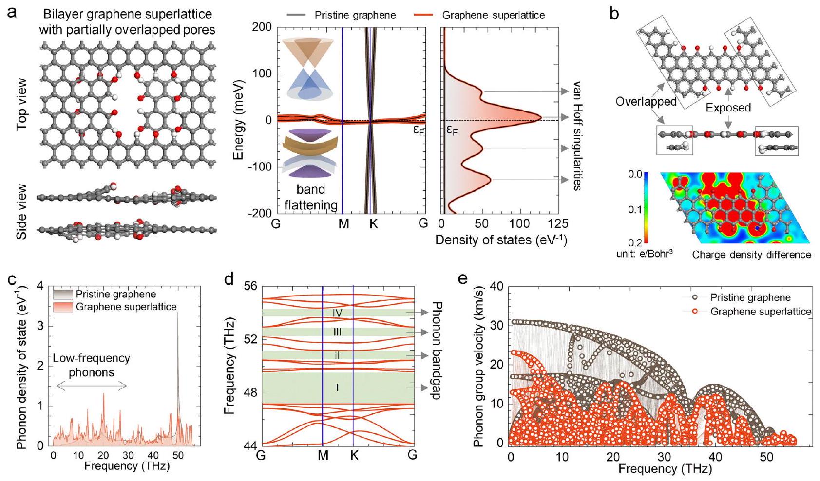
Electronic and phonon structure of graphene superlattice

We employed DFT calculations to compare the electronic structures of pristine bilayer graphene with graphene superlattices. Figure 2a illustrates that graphene superlattices exhibit a remarkable flattening of bands near the Fermi level, characterized by negligible band dispersion (less than 1 meV ). This flat-band structure arises from the weak dispersion relation of kinetic energy resulting from the periodic electronic reconstruction caused by atomic stress between the overlapped and exposed carbon regions, leading to the emergence of a new transition peak in X-ray absorption of the C K-edge (Supplementary Fig. 10 and Note 2). This electronic reconstruction leads to the formation of electron domain walls that confine Fermi electrons on either side, resulting in an equipotential Fermi surface and energy barriers with neighboring surfaces . The electron trapping effect leads to a closer proximity of valence electrons in graphene superlattice to the Fermi level, resulting in the formation of multiple van Hoff singularities , as demonstrated by the distribution of electronic density of states in Fig. 2b.
Dopants in graphene superlattices result in an elevated electronic density of states on both sides of the Fermi level, a notable enhancement of electron-electron interaction, and an intensified spin-orbit coupling , leading to a weakening of the dispersion relation between electrons and kinetic energy, resulting in an electron system with
Fig. 2 | Density functional theory (DFT) calculation of electronic and phonon structure of graphene superlattice. a Band structure and projected density of states of pristine graphene and graphene superlattice. represents the Fermi level. Arrows in (a) correspond to van Hoff singularities. b Charge density difference between the overlapped and exposed carbon atoms in graphene superlattice.
c-e Phonon density of states, phonon band structure, and phonon group velocity of graphene superlattice. The overlap ratio of nanopores in graphene superlattice, defined by the ratio of the pore area covered by a neighboring graphene layer to the total pore area, was set to 0.5 . The graphene superlattice was Te-doped. The green shaded areas, indicated by arrows in (d), represent the phonon bandgap.
infinite mass and an increased Coulomb interaction between electrons, thereby contributing to the enhanced band flattening. This computational analysis is supported by Hall carrier concentration measurements, revealing an approximate increase in carrier concentration and a significant 99.8% decrease in carrier mobility in graphene superlattices compared to pristine graphene (Supplementary Fig. 11). Computational study reveals that electronic band flattening is influenced by various factors, such as structural periodicity, types and ratios of the dopants, and pore geometries (Supplementary Figs. 12-16 and Note 3). Bilayer graphene with partially overlapped circular nanopores or totally overlapped square nanopores lacks a flatband structure due to the absence of a well-defined periodicity electron domain, attributing to the significant stress between the exposed and overlapped carbon atoms, which disrupts the formation of electron domain walls in these graphene structures.
We studied the effect of superlattice structure on the graphene phonon structure. Due to the harmonic oscillation of the atomic lattice , pristine graphene exhibits predominantly atom-propagated phonons with a frequency of 50 THz (Fig. 2c). In contrast, the periodic overlap of carbon atoms in bilayer graphene superlattices suppresses harmonic vibrations, leading to distinct phonon modes in the overlapped and exposed regions. The dopants at pore edges possess the same phonon vibrational modes that can give rise to clusters of new phonons , as evident by the vibrational density of states (Supplementary Fig. 17 and Note 4). The transmission of phonon clusters in graphene superlattices exhibits substantial coherent interference and elastic scattering , resulting in phonon cluster energy weakening and the emergence of a series of continuous standing waves in the lowfrequency range of , while the original high-frequency phonons disappear.
The absence of high-frequency phonons induces volume contraction of the first Brillouin zone, causing folding and compression of the phonon acoustic branches and resulting in phonon bandgaps in the high-frequency range , as compared to the pristine graphene (Fig. 2d and Supplementary Fig. 18). Calculations indicate that atomic participation ratios of graphene superlattices are lower than those of pristine graphene (Supplementary Fig. 19), confirming that a decrease in the proportion of atoms participating in the same phonon mode directly leads to a reduction in phonon energy and cluster velocities (Fig. 2e). The resulting localization of phonons and the electron trapping effect leads to strong electron-phonon coupling, wherein electrons absorb phonons, undergo motion, and scatter to excite new phonons . This continuous cycle gives rise to a prominent phonon drag effect, which significantly affects the trajectories and transport properties of electrons in graphene superlattice . In summary, the graphene superlattice exhibits remarkable quantum phase correlations at both the electron and phonon levels, resulting in a diverse range of functionalities that surpass those observed in pristine graphene. Our synthesis strategies pave the way for the design of 2D materials , especially 2D superlattices with tunable properties and unprecedented functionalities compared to pristine counterparts.

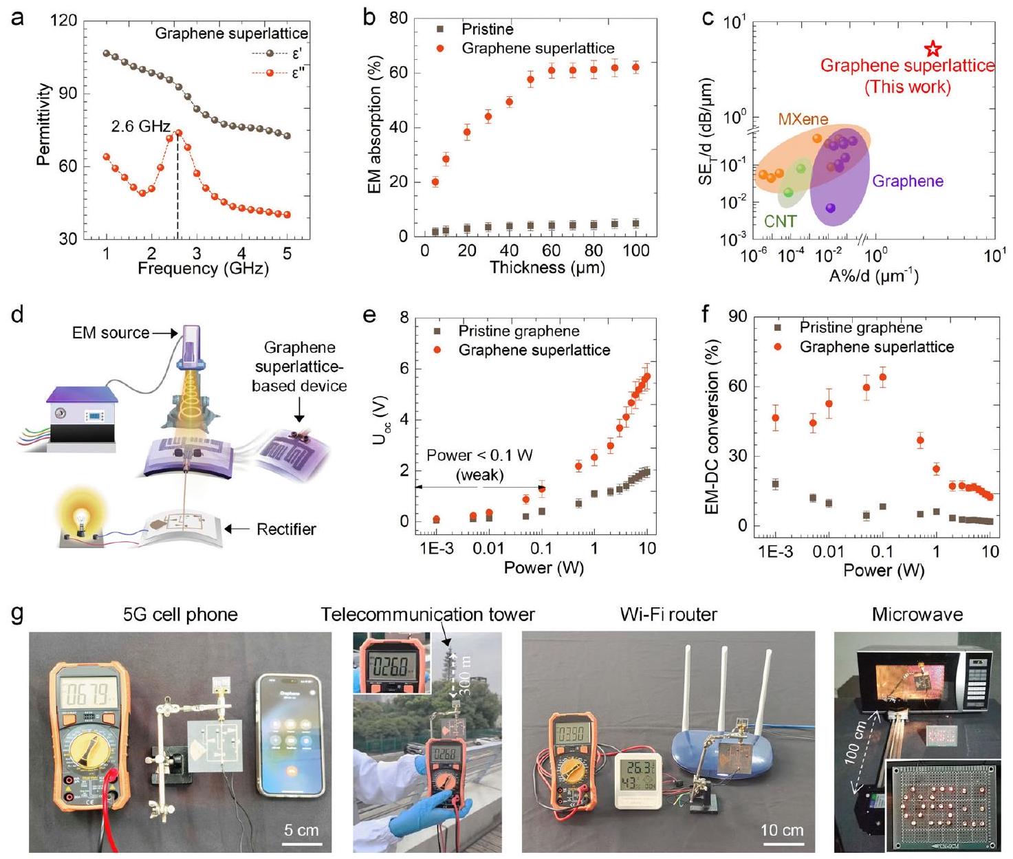
Electromagnetic wave modulation of graphene superlattice

The burgeoning advancements in wireless communications, particularly the fifth generation of mobile cellular network ( 5 G ), have raised concerns over the underutilization of EM waves and disruptive signal interference . Existing EM materials have limitations in their effectiveness, particularly with thicknesses of tens of micrometers. We investigate graphene superlattices to efficiently regulate EM waves and harness spatial EM energy. Figure 3a and Supplementary Fig. 20 demonstrate a remarkable dielectric dispersion behavior in the lowfrequency region, which corresponds to the current wireless communication band, observed in the element-doped graphene superlattice. This distinctive dielectric dispersion arises from an electronic reconfiguration triggered by atomic stress at the intersections
of both overlapping and exposed carbon regions. This reconfiguration initiates the creation of electron domain walls, effectively capturing Fermi electrons on both sides and generating an interfacial potential difference between adjacent surfaces. When subjected to altered EM fields, this potential dynamically reorients in response to the modified electric field, giving rise to a behavior of polarization relaxation. This relaxation behavior is characterized by a sharp decrease in real permittivity ( ) and a dielectric resonance peak in imaginary permittivity ( ), resulting in a substantial increase in EM absorption, effectively dissipating the EM waves as joule heat and minimizing EM wave reflection and secondary interference . We attribute this to the dielectric polarization relaxation, as demonstrated by the Cole-Cole curve (Supplementary Fig. 21 and Note 5), which arises from the periodic electron domain walls .
This dispersive behavior leads to an absorption efficiency of graphene superlattice in the region, within the thickness range of , that surpasses that of pristine graphene by two orders of magnitude (Fig. 3b). Even at a thickness of only , the absorption can exceed . Due to its high EM absorption coefficient, the average EM shielding effectiveness of graphene superlattice can reach 99.99% (corresponding to an EM shielding effectiveness ), effectively addressing secondary reflection-induced EM interference. The EM absorption capabilities of graphene superlattice in the micrometer thickness range surpass those of all existing EM materials (Supplementary Table 1). Direct comparison of EM shielding ability revealed that the EM shielding effectiveness and EM absorption efficiency per material thickness of graphene superlattice were two to four orders of magnitude higher than conventional 2D materials, including MXene and other chemically modified graphene, as shown in Fig. 3c. We demonstrated the ability to tune the EM absorption efficiency by adjusting the amounts of doped elements and shift the maximum EM absorption frequency by selecting the doped element type (Supplementary Fig. 22). This graphene superlattice selectively absorbs EM waves at a specific wavelength while allowing transmission of other bands, minimizing signal loss and offering potential integration into miniaturized circuits for efficient EM absorption.
The electron reconstruction triggered by the electronic domain not only impacts EM absorption but also notably reduces the relative complex permittivity ( ). This reduction significantly improves impedance matching, allowing incoming EM waves to penetrate the material more effectively, unlike the typical surface-skimming behavior observed with pristine graphene. In line with antenna design principles, our graphene superlattice film operates akin to an antenna, converting incoming waves into currents and generating a substantial electrical output. Figure 3d, along with Supplementary Figs. 23 and 24 and Note 6, elegantly illustrate the design and fabrication process of the graphene-superlattice device. As shown in Fig. 3e, the measured open circuit voltage ( ) of graphene superlattice increased from 0.1 V to 6.4 V with an increase in EM wave emission power from 1 mW to 10 W , respectively. The graphene superlattice-based device demonstrated a maximum power output of 0.31 W with a load resistance of when exposed to a 10 W source (Supplementary Fig. 25), and stable electricity output even after 1000 bending cycles or in different bending states (Supplementary Fig. 26). Furthermore, the overall efficiency of EM-DC conversion was calculated to be at an EM emission power of 100 mW , as shown in Fig. 3f. Notably, our device was able to efficiently harvest and convert EM waves from a 5 G cell phone, a wireless fidelity (Wi-Fi) router, a telecommunication tower, and a microwave to DC electricity that can be used to power electronic devices such as light-emitting diodes (LEDs) and digital hygro-thermometers, as shown in Fig. 3g and Supplementary Movies 1-4.

Expanded applications of graphene superlattice

Beyond EM modulation, graphene superlattices unveil unique electronic and phonon characteristics, suggesting potential applications in
Fig. 3 | Permittivity and electromagnetic wave modulation of graphene
superlattice. a Frequency-dependent permittivity of graphene superlattice. and represent the real and imaginary part of permittivity, respectively. The vertical dashed line marks the frequency corresponding to the dielectric loss peak.
b Thickness-dependent electromagnetic (EM) wave absorption efficiency of pristine bilayer graphene and graphene superlattice. Error bars represent standard deviations from three independent measurements on the same physical samples. c Comparison of EM shielding effectiveness ( ) and EM absorption efficiency ( ) averaged by EM absorbing material thickness of graphene superlattice with carbon nanotubes (CNTs) and other two-dimension (2D) materials. The data points compared in (c) are sourced from Supplementary References 82-96. d Experimental setup of graphene superlattice-based EM-electricity converter. e Open circuit
voltage ( ) and EM-electivity conversion of pristine graphene and graphene superlattice-based EM-electricity converter as a function of EM emission power. The EM-to-electricity conversion efficiency is defined as the ratio of power generated by a graphene device, which converts input EM energy into direct current, to the input EM power. Error bars represent standard deviations from three independent measurements on the same physical samples. g Photographs of EM-electricity conversion by graphene superlattice-based EM-electricity converter from a 5 G cell phone, a Wi-Fi router, a telecommunication tower, and a microwave (Supplementary Movies 1-4). The output DC electricity can be used to power electronic devices such as a digital hygro-thermometer and a collection of LEDs arranged in an ‘OSU’ pattern. The graphene superlattice was Te-doped.
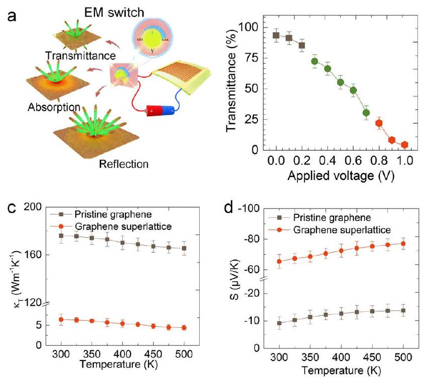
optics, electronics, and thermal sciences (see Supplementary Note 7 for detailed correlations). First, graphene superlattices exhibit multiple consecutive van Hoff singularities appear near the Fermi level (Fig. 2a). We developed a graphene superlattice-based smart EM wave window, which can selectively transmit, absorb, and shield EM waves by applying a voltage as low as 1.0 V (Fig. 4a). Second, in graphene superlattice, an increase in the energy level splitting and potential differences across the electron domain wall leads to the separation of electrons and holes, causing a remarkable photoluminescence effect within the visible light wavelength range ( ) in graphene superlattice, not being observed in pristine graphene (Fig. 4b). These findings highlight the high sensitivity of carrier transport in graphene superlattice with small bandgaps to external electric fields, making them promising candidates for applications in EM switch and optoelectronics.
Third, in the graphene superlattice, the presence of substantial coherent interference and phonon elastic scattering significantly diminishes in-plane lattice thermal conductivity, thereby leading to a
decrease in the overall thermal conductivity, as evidenced in Fig. 4c, Supplementary Fig. 27 and Note 8. This thermal conductivity, ranging between , constitutes only of the values observed in pristine graphene. This ultralow thermal conductivity not only provides desirable thermal insulation but also yields low infrared emissivity ( at the near-infrared band), making the graphene superlattice an ideal candidate for infrared stealth coatings (Supplementary Fig. 28). Furthermore, the combined effects of electron trapping and phonon drag significantly enhance the in-plane Seebeck coefficient of the graphene superlattice by compared to pristine graphene in the temperature range of (Fig. 4 d ). Meanwhile, the electrical conductivity decreased by only (Supplementary Fig. 29).
Current leading thermoelectric materials typically exhibit Seebeck coefficients within the range, only around two to four times the Seebeck coefficient of our developed graphene superlattice. However, they possess lower thermal conductivities, typically around , significantly less than our graphene superlattice. It is
Fig. 4 | Expanded applications of graphene superlattice. a Tunable EM transmission of a graphene superlattice-based smart window via applied voltage. Error bars indicate standard deviations from three independent measurements on the same physical samples. b Photoluminescence intensity comparison between pristine graphene and graphene superlattice. and represent the Fermi level and bandgap, respectively. represents the energy of a photon. Upward arrows indicate the direction of electron transition, while the dashed downward arrow represents the direction of an electron transitioning from a higher energy orbital to a lower energy orbital. c, d Temperature-dependent in-plane thermal conductivity
and in-plane Seebeck coefficient of pristine graphene and graphene superlattice. Error bars indicate standard deviations from three independent measurements on the same physical samples. e Comparison of in-plane figure of merit ( ) values of graphene superlattice with state-of-the-art thermoelectric materials. The data points compared in (e) are sourced from Supplementary References 92-126. The graphene superlattice was Te-doped. The graphene superlattice achieved a maximum of 0.33 , even at a low temperature of 500 K , surpassing pristine graphene by four orders of magnitude and demonstrating comparability to leading inorganic thermoelectric materials.
important to note that typical graphene materials differ significantly from leading thermoelectric materials in their Seebeck coefficient and thermal conductivity – the former often being two orders of magnitude lower and the latter three to four orders of magnitude higher. Yet, our graphene superlattice leads in electrical conductivity, surpassing traditional graphene by almost an order of magnitude. This substantial difference accentuates the thermoelectric performance of our graphene superlattice, resulting in remarkable in-plane figure-of-merit values up to 0.33 , even at a relatively modest temperature of 500 K (the effects on the out-of-plane parameters are detailed in Supplementary Figs. 29 and 30 and Note 9). This value is four orders of magnitude greater than pristine graphene, positioning our graphene superlattice among the most effective thermoelectric materials, as evidenced in Fig. 4e.

Discussion

We have chemically synthesized a nanoporous bilayer graphene superlattice with partially overlapping pores, revealing remarkable correlations between electron and phonon quantum phases and enabling diverse applications beyond pristine graphene, including ultrathin EM absorption, EM energy harvesting and conversion, thermoelectric performance at low-to-intermediate temperatures, photoluminescence, and optoelectronic devices. Our study provides a chemical principle for the design and synthesis of a unique family of 2D superlattices, expanding our understanding of these structures and paving the way for the development of cutting-edge technologies. Future research efforts will focus on precise control of the lattice mismatching in nanoporous graphene sublattices to gain insights into their influence on the unique properties and functionalities of the superlattice. Our methodology can be extended to the creation of 2D superlattices using other conventional 2D materials, further broadening the range of materials including 2D and porous materials with tailored properties and diverse applications.

Methods

Materials

Iron acetylacetonate, oleic acid, oleyl amine, ammonia ( in water), hydrogen peroxide ( in water), sodium chloride, sodium molybdate dehydrate, thiourea, ferrous chloride, cobalt acetate, ethylene glycol, zinc acetate, lanthanum oxide, cobalt nitrate, tetraethyl orthosilicate, sodium hydroxide, oxalic acid, strontium carbonate, cobalt oxalates, bismuth nitrate pentahydrate, diboron trioxide, 1-butyl-3-methlyimidazolium hexafluorophosphate ( ), silver nitrate, stannous chloride, sulfur powder, ethylenediaminetetraacetic acid disodium, copper nitrate, hexadecyltrimethylammonium bromide, formaldehyde, mercury oxide, mercury, cyclohexane, isopropanol, iron pentacarbonyl, 1,3-dimethylimidazoline-2-selenone, hydrochloric acid ( in water), tellurium power, selenium powder, potassium hydroxide, sulfuric acid and sulfide powder were purchased from Sigma-Aldrich. Raw graphene and multiwall carbon nanotubes were obtained from XF-NANO Tech. Co. All chemical reagents are analytical pure reagents and were used without further purification. Polydimethylsiloxane (PDMS) film was purchased from Shanghai Muke Technol. Co. Deionized water used in all the experiments was purified using a Simplicity C9210 Milli-Q water purification system.

Synthesis of graphene superlattice

Initially, a mixture of iron acetylacetonate ( 1.4 g ), raw bilayer graphene synthesized via chemical vapor deposition (CVD), oleic acid , and oleyl amine was prepared and stirred for 30 min . The mixture was then heated under a nitrogen flow at a temperature range of with vigorous stirring for 2 h . Subsequently, the temperature was increased to at a heating rate of and held for 30 min , followed by heating to for an additional 30 min at a rate of . After cooling to room temperature, the graphene coated with cubic nanoparticles was collected by centrifugation
after dispersion in cyclohexane and isopropanol. The obtained graphene coated with cubic nanoparticles was subjected to a heat treatment at for 60 min under a continuous nitrogen flow to remove organic solvents. Subsequently, the temperature was gradually increased to at a rate of and maintained for 0.5 h to induce the formation of square-shaped nanometer-sized pores on the bilayer graphene surface. After cooling, the graphene was dispersed in a hydrochloric acid solution with a pH of to remove the coated nanoparticles, resulting in the formation of squared nanopores. By employing raw graphene with different layer numbers, porous graphene with various layer numbers can be fabricated.

Synthesis of graphene with completed overlapped nanopores

We produced graphene with fully overlapped nanopores using a bottom-up approach involving the thermal decomposition of oleic acid iron-coated sodium chloride ( NaCl ) particles. Initially, 0.1 g of NaCl particles, ranging from 5 to , were submerged in 10 mL of oleic acid iron solution. This step ensures the adsorption of the oleic acid iron onto the NaCl particles, resulting a coated layer of oleic acid iron on the NaCl surface. During thermal decomposition at with a nitrogen gas flow, the iron oleate on the NaCl surface undergoes a transformation into cubic nanoparticles. Simultaneously, carbon sheets form, encapsulating these cubic nanoparticles and incorporating the into carbon nanosheets. Subsequent to the thermal decomposition, the composite material is immersed in water to dissolve and remove the NaCl substrate. An acid wash follows, selectively extracting the , resulting in the production of aligned, porous carbon nanosheets. Lastly, graphene with completely overlapped nanopores was obtained by drying in a vacuum oven for 12 hours, followed by thermal reduction at for 2 hours in a hydrogen gas flow.
Selective element doping at pore edges of graphene superlattice To achieve selective doping of elements at the pore edges of the graphene superlattice, a stepwise annealing process was employed. The graphene superlattice was subjected to annealing at , and for 1 h to progressively decompose the , and -COOH groups at the pore edges, respectively. The first two annealing steps were carried out under a nitrogen gas flow, while the final step was conducted in a mixture gas consisting of hydrogen and 95 nitrogen. Selective doping of O and H at the pore edges of the bilayer porous graphene was achieved after the second and third step ( ) of annealing, respectively. Furthermore, the selective doping of other elements such as , and Se at the pore edges of graphene was achieved through thermal decomposition at various temperatures (Supplementary Table 2).

Structural characterization of porous graphene

Graphene superlattice phase identification was conducted using a Bruker D8 ADVANCE XRD equipped with radiation (wavelength of 0.15406 nm ). The morphology of the nanoparticles and porous graphene was investigated using a Joel JEM 2100 F transmission electron microscope (TEM) with a 200 kV field emission. X-ray photoelectron spectroscopy (XPS) analyses were carried out using an Escalab 250Xi spectrometer. The graphitization quality was evaluated using a Jobin Yvon HR 800 confocal Raman spectroscope. Synchrotron X-ray absorption near-edge structure (XANES) analysis was performed at Beamline 33BM-C in the XOR Division of the Advanced Photon Sources. Extended X-ray absorption measurements were conducted at beamline 7-BM of the National Synchrotron Light Source II, Brookhaven National Laboratory. Chemical bonding analysis of graphene was carried out using a Nicolet iS50 Fourier Transform Infrared Spectrometer (FT-IR). Photoluminescence performance was recorded at room temperature using a LifeSpec II fluorescence lifetime spectrometer
equipped with a diode laser emitting at a wavelength of 365 nm . Infrared emissivity was measured using a PerkinElmer Spotlight 200i FT-IR spectrometer along with an IR integrating sphere.

Evaluation of electromagnetic shielding and absorption of graphene superlattice

The EM frequency-dependent scattering parameters (i.e., and ) and permittivity of graphene were measured via the single coaxial-line method using an Agilent PNA N5224A vector network analyzer. The corresponding absorption efficiency ( ) and shielding effectiveness can be calculated as :
We note here that the uncertainty in the permittivity and scattering parameter measurements is about due to variations originating from the smoothness of sample surfaces.

Characterization of in-plane thermal conductivity, electric conductivity and Seebeck coefficient of graphene superlattice

To obtain the in-plane Seebeck coefficient and electrical conductivity, a precise amount of bilayer graphene powder was dispersed in an ethanol solution. A film approximately thick was created using vacuum filtration. This filtered film was shaped into strips measuring in length and width. Around 15 of these strips were oriented and stacked to form a film with 3 mm thick. The Seebeck coefficient and electrical conductivity were evaluated along the length of the film using the ULVAC-RIKO ZEM-3 apparatus in a helium atmosphere at a heating rate of .
To assess the in-plane thermal conductivity, the filtered film was sectioned into strips measuring 15 mm in length and 5 mm in width. Approximately fifty of these strips were stacked to create a film approximately 10 mm thick. Heat conduction was directed along the length of the stacked film during the evaluation using the Netzsch HFM446 heat flow thermal instrument, ensuring precise measurement of in-plane thermal conductivity. Based on the in-plane Seebeck coefficient, electrical conductivity, and thermal conductivity, figure of merit (ZT) was calculated as :
where represents electrical conductivity, denotes the Seebeck coefficient, corresponds to thermal conductivity, and is the temperature.

Data availability

Relevant data supporting the key findings of this study are available within the article and the Supplementary Information file. All raw data generated during the current study are available from the corresponding authors upon request.

References

  1. Zhou, J. et al. Heterodimensional superlattice with in-plane anomalous hall effect. Nature 609, 46-51 (2022).
  2. Cao, Y. et al. Unconventional superconductivity in magic-angle graphene superlattices. Nature 556, 43 (2018).
  3. Chen, D. et al. Excitonic insulator in a heterojunction moiré superlattice. Nat. Phys. 18, 1171-1176 (2022).
  4. Septianto, R. et al. Enabling metallic behavior in two-dimensional superlattice of semiconductor colloidal quantum dots. Nat. Commun. 14, 2670 (2023).
  5. Chen, P. et al. Chemical synthesis of two-dimensional atomic crystals, heterostructures and superlattice. Chem. Soc. Rev. 467, 3129 (2018).
  6. Pantaleon, P. A. et al. Superconductivity and correlated phases in non-twisted bilayer and trilayer graphene. Nat. Rev. Phys. 5, 304-315 (2023).
  7. Zhang, Z. W. et al. Robust epitaxial growth of two-dimensional heterostructures, multi-heterostructures, and superlattices. Science 357, 788 (2017).
  8. Zhang, S. et al. Domino-like stacking order switching in twisted monolayer-multilayer graphene. Nat. Mater. 21, 621 (2022).
  9. Geuchies, J. J. et al. In-situ study of the formation mechanism of two-dimensional superlattices from PbSe nanocrystals. Nat. Mater. 15, 1248 (2016).
  10. Huang, T. Y. et al. Observation of chiral and slow plasmons in twisted bilayer graphene. Nature 605, 63 (2022).
  11. Shen, C. et al. Dirac spectroscopy of strongly correlated phases in twisted trilayer graphene. Nat. Mater. 22, 316 (2023).
  12. Merida, J. D. et al. Symmetry-broken josephson junctions and superconducting diodes in magic-angle twisted bilayer graphene. Nat. Commun. 14, 2396 (2023).
  13. Zhang, Y. et al. Every-other-layer dipolar excitons in a spin-valley locked superlattice. Nat. Nanotechnol. 18, 501 (2023).
  14. Chio, S. H. et al. Large-scale synthesis of graphene and other 2D materials towards industrialization. Nat. Commun. 13, 1484 (2022).
  15. Xu, F. et al. Atomic Sn-enabled high-utilization, large-capacity, and long-life Na anode. Sci. Adv. 8, eabm7489 (2022).
  16. Cui, J. et al. Supermolecule cucurbituril subnanoporous carbon supercapacitor (SCSCS). Nano Lett. 21, 2156-2164 (2021).
  17. Ghorashi, S. A. et al. Topological and stacked flat bands in bilayer graphene with a superlattice potential. Phys. Rev. Lett. 130, 196201 (2023).
  18. Hu, H. et al. Doping-driven topological polaritons in graphene/ heterostructures. Nat. Nanotechnol. 17, 940 (2022).
  19. Chen, W. et al. Heteroatom-doped flash graphene. ACS Nano 16, 6646 (2022).
  20. Bie, C. et al. Design, fabrication, and mechanism of nitrogen-doped graphene-based photocatalyst. Adv. Mater. 33, 2003521 (2021).
  21. Choi, Y. W. et al. Dichotomy of electron-phonon coupling in graphene Moiré flat bands. Phys. Rev. Lett. 127, 167001 (2021).
  22. Wei, K. et al. Acoustic phonon recycling for photocarrier generation in graphene- heterostructures. Nat. Commun. 11, 3876 (2020).
  23. Sadeghi, M. et al. Tunable electron-flexural phonon interaction in graphene heterostructures. Nature 617, 282 (2023).
  24. Lian, B. et al. Twisted bilayer graphene: a phonon-driven superconductor. Phys. Rev. Lett. 122, 257002 (2019).
  25. Bodapati, A. et al. Vibrations and thermal transport in nanocrystalline silicon. Phys. Rev. B. 24, 74 (2006).
  26. Nathawat, J. et al. Signatures of hot carriers and hot phonons in the re-entrant metallic and semiconducting states of Moire-gapped graphene. Nat. Commun. 14, 1507 (2023).
  27. Gadelha, A. et al. Localization of lattice dynamics in low-angle twisted bilayer graphene. Nature 590, 405 (2021).
  28. Li, J. et al. 2D MOF periodontitis photodynamic ion therapy. J. Am. Chem. Soc. 143, 15427-15439 (2021).
  29. Hu, T. et al. Layered double hydroxide-based nanomaterials for biomedical applications. Chem. Soc. Rev. 51, 6126 (2022).
  30. Iqbal, A. et al. Anomalous absorption of electromagnetic waves by 2D transition metal carbonitride (MXene). Science 369, 446 (2020).
  31. Lv, H. et al. A flexible electromagnetic wave-electricity harvester. Nat. Commun. 12, 834 (2021).
  32. Wu, Y. et al. Broadband multispectral compatible absorbers for radar, infrared and visible stealth application. Prog. Mater. Sci. 135, 101088 (2023).
  33. Xia, Y. et al. A review on graphene-based electromagnetic functional materials: electromagnetic wave shielding and absorption. Adv. Funct. Mater. 32, 2204591 (2022).
  34. Ji, X. et al. Capturing functional two-dimensional nanosheets from sandwich-structure vermiculite for cancer theranostics. Nat. Commun. 12, 1124 (2021).
  35. Meng, J. et al. Universal approach to fabricating graphenesupported single-atom catalysts from doped ZnO solid solutions. ACS Cent. Sci. 6, 1431 (2020).
  36. Zhu, Y. et al. Emerging porous organic polymers for biomedical applications. Chem. Soc. Rev. 51, 1377 (2022).
  37. Wu, J. et al. Porous polymers as multifunctional material platforms toward task-specific applications. Adv. Mater. 31, 1802922 (2019).
  38. Cui, J. et al. Ganoderma Lucidum-derived erythrocyte-like sustainable materials. Carbon 196, 70 (2022).
  39. Zheng, B. et al. Emerging functional porous polymeric and carbonaceous materials for environmental treatment and energy storage. Adv. Funct. Mater. 30, 1907006 (2020).
  40. Xie, Y. et al. Synergistic cobalt sulfide/eggshell membrane carbon electrode. ACS Appl. Mater. Interfaces 11, 32244 (2019).
  41. Zhang, Y. et al. Controlled distributed hollow microspheres on thermally conductive polyimide composite films for excellent electromagnetic interference shielding. Adv. Mater. 35, 2211642 (2023).
  42. Lv, H. et al. Staggered circular nanoporous graphene coverts electromagnetic waves into electricity. Nat. Commun. 14, 1982 (2023).
  43. Zheng, Z. H. et al. Harvesting waste heat with flexible thermoelectric thin film. Nat. Sust. 6, 180 (2023).

Acknowledgements

X.W. would like to acknowledge the financial support from the startup fund of The Ohio State University (OSU), OSU Sustainability Institute Seed Grant, OSU Materials Research Seed Grant Program, funded by the Center for Emergent Materials, an NSF-MRSEC, grant DMR-2011876, the Center for Exploration of Novel Complex Materials, and the Institute for Materials Research.

Author contributions

H.L., R.W., C. Z.; R.C., S.A., M.Y., X. Zhang, and X.W. conceived and designed the experiments, supervised the research, and contributed to manuscript writing. H.L., M.Y., Y.Y., S.L., R.L.D., U.I.K., B.C., C.Z., X.Zhou, Y.W., and R.W. conducted material synthesis and performed various characterizations. C.Z., Y.W. and L.R. designed the graphene device and measured its EM-electricity output. H.L., L.R., B.C., and X.Zhou conducted permittivity, thermal conductivity, Hall effect, and Seebeck characterizations. H.L. and B.L. performed molecular dynamics simulations. G.C. and B.L. carried out first-principles density functional theory simulation and modular dynamic analysis. All authors contributed to data interpretation, discussions, and manuscript preparation. H.L., Y.Y., M.Y., G.C., and Y.W. contributed equally to this work.

Competing interests

The authors declare no competing interests.

Additional information

Supplementary information The online version contains
supplementary material available at
https://doi.org/10.1038/s41467-024-45503-9.
Correspondence and requests for materials should be addressed to Cheng Zhang, Renbing Wu, Renchao Che, Xingcai Zhang or Xiaoguang Wang.
Peer review information Nature Communications thanks Wenzhuo Wu and the other, anonymous, reviewer for their contribution to the peer review of this work. A peer review file is available.
Reprints and permissions information is available at
http://www.nature.com/reprints
Publisher’s note Springer Nature remains neutral with regard to jurisdictional claims in published maps and institutional affiliations.
Open Access This article is licensed under a Creative Commons Attribution 4.0 International License, which permits use, sharing, adaptation, distribution and reproduction in any medium or format, as long as you give appropriate credit to the original author(s) and the source, provide a link to the Creative Commons license, and indicate if changes were made. The images or other third party material in this article are included in the article’s Creative Commons license, unless indicated otherwise in a credit line to the material. If material is not included in the article’s Creative Commons license and your intended use is not permitted by statutory regulation or exceeds the permitted use, you will need to obtain permission directly from the copyright holder. To view a copy of this license, visit http://creativecommons.org/ licenses/by/4.0/.
© The Author(s) 2024

  1. William G. Lowrie Department of Chemical and Biomolecular Engineering, The Ohio State University, Columbus, OH 43210, USA. Institution of Optoelectronic, Laboratory of Advanced Materials, Academy for Engineering & Technology, Department of Materials Science, Fudan University, Shanghai 200438, P. R. China. Department of Chemistry and Chemical Biology, Harvard University, Cambridge, MA O2138, USA. Division of Chemistry and Chemical Engineering, California Institute of Technology, Pasadena, CA 91125, USA. Key Laboratory of Materials for High-Power Laser, Shanghai Institute of Optics and Fine Mechanics, Chinese Academy of Sciences, Shanghai 201800, P. R. China. School of Engineering, Massachusetts Institute of Technology, Cambridge, MA 02139, USA. College of Mechanical and Vehicle Engineering, Hunan University, Changsha 410082, P. R. China. Department of Mechanical Engineering, University of Michigan, Ann Arbor, MI 48109, USA. School of Engineering and Applied Sciences, Harvard University, Cambridge, MA 02138, USA. Sustainability Institute, The Ohio State University, Columbus, OH 43210, USA. e-mail: czhangseu@foxmail.com; rbwu@fudan.edu.cn; rcche@fudan.edu.cn; zhangxingcai@wteao.com; wang.12206@osu.edu