الميمريستورز ذات التبديل فائق السرعة المستندة إلى المواد ثنائية الأبعاد Ultra-fast switching memristors based on two-dimensional materials

المجلة: Nature Communications، المجلد: 15، العدد: 1
DOI: https://doi.org/10.1038/s41467-024-46372-y
PMID: https://pubmed.ncbi.nlm.nih.gov/38485722
تاريخ النشر: 2024-03-14

الميمريستورز ذات التبديل فائق السرعة المستندة إلى المواد ثنائية الأبعاد

تاريخ الاستلام: 9 مارس 2023
تاريخ القبول: 26 فبراير 2024
تاريخ النشر على الإنترنت: 14 مارس 2024
(D) تحقق من التحديثات

S. S. Teja Nibhanupudi © , أنوبام روي (B) , ديمتري فيكسلر , ماثيو كوين © , كيفن سي. ماثيوز © , ماثيو ديسينا , أنش¹، جاتين في. سينغ © , لوانا ر. جيربا-دولوكان , جيمي وارنر , جاي ديب ب. كولكارني، جينادي بيرسوكير & سانجاي ك. بانيرجي

الملخص

تقدم القدرة على تقليل سمك المواد ثنائية الأبعاد (2D) إلى طبقة أحادية فرصة واعدة لتحقيق متغيرات سريعة وفعالة من حيث الطاقة. هنا، نبلغ عن متغير سريع للغاية تم تصنيعه باستخدام أوراق رقيقة ذرية من نيتريد البورون السداسي ثنائي الأبعاد، مما يظهر أسرع سرعة تبديل تم ملاحظتها (120 بيكو ثانية) بين المتغيرات ثنائية الأبعاد وطاقات تبديل منخفضة (2 بيكو جول). علاوة على ذلك، ندرس ديناميات التبديل لهذه المتغيرات باستخدام نبضات جهد فائقة القصر ( )، وهو نطاق تردد ذو صلة كبيرة في سياق الدوائر الحديثة من أشباه الموصلات المعدنية المؤكسدة التكميلية (CMOS). نستخدم التحليل الإحصائي للخصائص العابرة للحصول على رؤى حول آلية تبديل المتغير. تؤكد بيانات التحمل الدائري على قدرة التبديل السريعة للغاية لهذه المتغيرات، مما يجعلها جذابة لتطبيقات الحوسبة والتخزين والدوائر ذات الترددات الراديوية (RF) من الجيل التالي.

في عصر الرقمية اليوم، أصبح دور تقنية الذاكرة جزءًا لا يتجزأ، خاصة في سياق تطبيقات الذكاء الاصطناعي (AI). تعتمد العديد من مهام الذكاء الاصطناعي، مثل التصنيف، والتعرف، ومعالجة اللغة الطبيعية، والتنبؤ، وما إلى ذلك، بشكل كبير على قدرة التخزين والمعالجة الكبيرة للذاكرة في الأجهزة الأساسية . تعتبر تقنيات الذاكرة التقليدية مثل ذاكرة الوصول العشوائي الثابتة (SRAM) أو ذاكرة الوصول العشوائي الديناميكية (DRAM) غير فعالة من حيث الطاقة لتنفيذ هذه التطبيقات التي تتطلب بيانات كثيفة بسبب طبيعتها المتقلبة، مما يؤدي إلى فقدان الطاقة الديناميكية والثابتة. هذه المتطلبات الطاقية أكثر صرامة للأجهزة المحمولة، والالكترونيات القابلة للارتداء، وأجهزة إنترنت الأشياء (IoT) التي تعمل بالبطارية . على الرغم من أن الذاكرة الفلاش غير متقلبة، فإن سرعة البرمجة البطيئة ( ميكروثانية) تجعلها غير عملية لهذه التطبيقات . للاستفادة بشكل فعال وتعظيم إمكانيات الذكاء الاصطناعي وغيرها من التطبيقات الناشئة، فإن ذاكرة غير متقلبة سريعة للغاية ضرورية.
تعتبر المتغيرات أجهزة واعدة في مشهد الذاكرة غير المتقلبة الناشئة التي أظهرت إمكانيات كبيرة بفضل حجمها الصغير ( )، وسرعة التشغيل، واستهلاك الطاقة المنخفض .
استكشفت العديد من الدراسات استخدام المتغيرات للتخزين، والحوسبة المتركزة على الذاكرة ، وتطبيقات RF عالية التردد . في العقد الماضي، تم تصنيع المتغيرات باستخدام مجموعة متنوعة من المواد مثل أكاسيد المعادن الانتقالية (TMO) ، والكالكوجينيدات ، والمواد العضوية وقد تم دراستها بشكل مكثف. أثبتت دراسات TEM بشكل قاطع أن التبديل المقاوم في المتغيرات يمكن أن يُعزى إلى وجود خيوط نانوية موصلة . بناءً على الملاحظات التجريبية، تم التقاط ديناميات التبديل في المتغيرات باستخدام تقنيات نمذجة مختلفة . عادةً ما تتبدل المتغيرات المتاحة تجاريًا في النطاق، مما يجعلها أبطأ من DRAM المتطورة . على الرغم من أن بعض الدراسات قد أفادت بوجود متغيرات أسرع في التبديل ( ، إلا أن ديناميات التبديل السريعة لم يتم دراستها بشكل شامل.
هنا، نقدم متغيرًا سريعًا للغاية تم تصنيعه باستخدام مادة ثنائية الأبعاد (2D)، أي نيتريد البورون السداسي (hBN) كطبقة تبديل . تسهل الطبيعة الرقيقة ذرية للمادة ثنائية الأبعاد ديناميات خيوط سريعة مما يمكّن من متغير سريع وفعال من حيث الطاقة. ندرس هذه المتغيرات باستخدام نبضات فائقة القصر
( ) في إعداد اختبار RF مصمم خصيصًا. علاوة على ذلك، نظرًا لأن تشكيل/ذوبان الخيوط في المتغيرات هو عملية عشوائية ، فإننا نستخدم التحليل الإحصائي للخصائص العابرة لدراسة هذه المتغيرات. قدمت البيانات الإحصائية رؤى حاسمة حول آلية التبديل والعشوائية الكامنة في ديناميات الخيوط. على حد علمنا، هذه هي الدراسة الأولى من نوعها ليس فقط في المتغيرات ثنائية الأبعاد ولكن بين العديد من التقارير العلمية المستندة إلى متغيرات TMO. بالإضافة إلى ذلك، من خلال الاستفادة من الإشارات من البيانات الإحصائية، نقوم بنمذجة ديناميات التبديل السريعة باستخدام مزيج من حل الفيزياء القائم على العناصر المحدودة، والمعادلات التجريبية، والتحليلية.

النتائج

تصنيع الجهاز والأداء الكهربائي المستمر

تظهر الميزات الهيكلية للمتغير المصنع مع طبقات hBN متعددة الطبقات المحصورة بين أقطاب نشطة (Ti) وغير نشطة (Au) في الشكل 1a، b. تم تصنيع طبقات hBN المتبدلة باستخدام ترسيب البخار الكيميائي (CVD) على ورق نحاسي وتم نقلها إلى ركيزة لتصنيع الجهاز (انظر الشكل التكميلي 1 وقسم الطرق للحصول على التفاصيل). تم تأكيد الهيكل النهائي للجهاز باستخدام المجهر الإلكتروني الماسح (SEM) (الشكل 1c) وصور المجهر الإلكتروني الناقل المقطعي (TEM) (الشكل 1d). تتكون أفلام hBN المصنعة من 7-8 طبقات بسمك مع مسافة بين الطبقات تبلغ 0.33 نانومتر، كما يتضح من صور TEM (الشكل التكميلي 2،3). تحتوي هذه الأفلام المزروعة بواسطة CVD على عيوب داخلية بعرض ذرة واحدة وذرات قليلة، كما هو موضح في الشكل 1e. تسهل هذه العيوب تشكيل خيوط موصلة، مما يمكّن بدوره من سلوك التبديل المقاوم المطلوب. من الجدير بالذكر أن الدراسات السابقة قد أفادت بعدم وجود ظاهرة تبديل مقاوم في الرقائق المتقشرة التي تفتقر إلى العيوب الداخلية . تم تأكيد التركيب البلوري والتركيب الكيميائي لأفلام hBN المصنعة باستخدام تقنيات مطياف رامان ومطياف الأشعة السينية (XPS) (الشكل التكميلي 4). بالإضافة إلى ذلك، تم دراسة المتغيرات المصنعة بأفلام hBN أرق ( طبقات) (الشكل التكميلي 5)، المصنعة عن طريق ضبط معلمات النمو للمقارنة.
تم تصنيع أجهزة بمساحات مقطع عرضي مختلفة تتراوح من إلى (الشكل التكميلي 6) وتم تصنيفها. تظهر الغالبية العظمى من الأجهزة المصنعة (العذراء) ( ) مقاومة عالية ( )، مما يشير إلى الجودة الممتازة لأفلام hBN المصنعة (الشكل التكميلي 7.1). من المحتمل أن تحتوي الأجهزة المتبقية
ذات المقاومة الأولية المنخفضة على حدود حبيبية أو عيوب بعرض عدة ذرات تم إدخالها على الأرجح أثناء عمليات التصنيع. تم التخلص من هذه الأجهزة المتسربة ولم تؤخذ في الاعتبار لمزيد من التحليل. يولد الجهد العالي المطبق على القطب Ti أثناء عملية التشكيل الخيط الموصل داخل المتغير. يظهر الشكل التكميلي 7.2 أن مقدار جهد التشكيل مرتبط مباشرة بالمقاومة الأولية للمتغير. وبالتالي، تتطلب الأجهزة ذات المقاومة الأولية الأعلى، المميزة بعيوب أقل، جهدًا أعلى لتأسيس الخيط الموصل. من الواضح أن هذا الاتجاه صحيح لجميع الأجهزة، بغض النظر عن مقطع الجهاز العرضي. لضمان أن المقاومة الأولية المقاسة والتبديل المقاوم اللاحق لم تتأثر بطبقة غير مقصودة عند الواجهة (طبقة Ti القابلة للأكسدة)، تم قياس الأجهزة المصنعة بدون طبقة hBN (الشكل التكميلي 8). تظهر هذه الأجهزة توصيلًا أومياً بمقاومة منخفضة ( )، مما يؤكد عدم وجود أي طبقة كبيرة.
بعد عملية التشكيل، تظهر المتغيرات خصائص تبديل مقاوم ثنائي القطب مع تطبيق جهد إيجابي وسلبي على القطب العلوي Ti لعمليات SET (الانتقال إلى مقاومة أقل) وRESET (الانتقال إلى مقاومة أعلى)، على التوالي. يظهر الشكل 2a عمليات سحب التيار المستمر ( ) التمثيلية لجهاز المتغير مع حد امتثال للتيار قدره . يتم تقديم عمليات السحب الإضافية ( ) المقاسة من عدة أجهزة في الشكل التكميلي 9. البيانات المجمعة من 200 مثل هذه تم تحليل الآثار لتحديد كمية التغير في خصائص الجهاز. تُظهر التحليلات الإحصائية أن الحد الأدنى للفصل بين حالة المقاومة العالية (HRS) وحالة المقاومة المنخفضة (LRS) هو ~50x (الشكل 2b)، مع الأخذ في الاعتبار التغيرات. وبالمثل، يتميز التغير في جهدي SET وRESET بتوزيعات غاوسية ذات قيم متوسطة ( ) من 1.73 فولت و -0.85 فولت، على التوالي (الشكل 2c). يظهر توزيع جهد SET تشتتًا أعلى (الانحراف المعياري ( ) من 0.5 فولت ) يُعزى بشكل رئيسي إلى التباينات بين الأجهزة (انظر الشكل التوضيحي 10 للمناقشة). بالمقارنة، فإن توزيع جهد إعادة الضبط ضيق إلى حد ما مع من 0.27 فولت. يمكن تقليل هذا التغير في جهد التبديل بشكل أكبر من خلال ضمان جودة بلورية عالية للمادة ثنائية الأبعاد المُصنَّعة ومن خلال استخدام طرق تصنيع أجهزة متفوقة يمكن أن تقلل من خشونة سطح الأقطاب.
لدراسة آليات النقل المسؤولة عن عملية التبديل، SET تم رسم المسح على مقياس لوغاريتمي-لوغاريتمي
الشكل 1 | هيكل الجهاز لمقاوم الذاكرة ثنائي الأبعاد hBN المُصنّع. أ رسم تخطيطي لجهاز مقاوم الذاكرة. مخطط مقطع عرضي يوضح الاتصال المعدني المستخدم للأقطاب العلوية (تيتانيوم) والسفلية (ذهب). ج صورة SEM للجهاز بعد التصنيع (صورة مصغرة) صورة مكبرة حيث الأقطاب العلوية والسفلية.
صورة TEM بتباين الطور للجهاز تُظهر مقطع عرضي بسمك 8 طبقات من hBN محصورة بين أقطاب معدنية. e مقطع TEM مكبر يُظهر الهيكل الطبقي لـ hBN مع عيوب بذرّة واحدة (أسهم) ومناطق غير متبلورة بعرض بضع ذرات (دوائر متقطعة).
الشكل 2 | توصيف التيار المستمر لميمريستور hBN ثنائي الأبعاد. أ التيار المستمر تظهر مسحات الذاكرة الهجينة من نوع hBN لمدة 20 دورة متتالية (تظهر منحنيات التعيين باللون الأحمر ومنحنيات إعادة التعيين باللون الأزرق). توزيع الاحتمالات التراكمية للمقاومة في حالات HRS و LRS المستخرجة من عمليات السحب المستمر DC تم جمعه من آثار. ج توزيع جهد SET/RESET باستخدام تيار التوافق 100 ميكروأمبير. د منحنى I-V لـ SET مرسوم على مقياس لوغاريتمي-لوغاريتمي يظهر مناطق ذات ميل متغير في HRS وميل خطي في LRS. هـ مسح الجهاز في LRS تم قياسه عند درجات حرارة تشغيل مختلفة (225 كلفن (المنحنى الوردي)، 250 كلفن (المنحنى الأسود)، 275 كلفن (المنحنى الأزرق)، 300 كلفن (المنحنى الأحمر))؛ (الإدراج) المقاومة المستخرجة عند مخطط مقابل
درجة الحرارة. يحتوي الميمريستور في حالة المقاومة المنخفضة على معامل حرارة إيجابي للمقاومة مما يشير إلى تكوين خيوط معدنية. ) مسحات الجهاز في HRS تم قياسها عند درجات حرارة تشغيل مختلفة ( ); (إدراج) المقاومة المستخرجة عند (المنحنى الأسود)، 0.75 فولت (المنحنى الأزرق)، 1 فولت (المنحنى الأحمر) تم رسمها مقابل درجة الحرارة. تقليل المقاومة مع زيادة درجة الحرارة يشير إلى التوصيل من خلال وسط عازل. صورة مقطع عرضي TEM توضح المواقع التي تم جمع ملف طيف فقدان طاقة الإلكترون (EELS) منها. النقاط A (المنحنى الأحمر)، D (المنحنى الأسود) تقع داخل قطب الذهب، النقطة B (المنحنى الأزرق) تقع داخل طبقة hBN، والنقطة C (المنحنى الأخضر) داخل قطب التيتانيوم.
(الشكل 2d). الجهاز الذي ينتقل إلى حالة المقاومة المنخفضة (LRS) أثناء عملية الضبط (SET) يمر عبر مناطق توصيل ذات انحدارات متغيرة، مما يشير إلى أن آلية نقل الشحنة السائدة تتغير: التوصيل الأومى مع انحدار التوصيل المحدود بشحنة الفضاء (SCLC) في المناطق ذات الميل وحدود ملء الفخ SCLC في المناطق ذات الانحدار تؤكد عمليات سحب الجهد ثنائية الاتجاه أن التغير في الميل قابل للعكس، وبالتالي، ليس مرتبطًا بتكوين الخيوط (الشكل التكميلي 11). يؤدي زيادة الجهد بشكل أكبر إلى قفزة مفاجئة في التيار (الميل ) مما يشير إلى تشكيل خيوط موصلة أومية (ميل ). الامتثال الحالي يمنع المزيد من توسيع الخيوط ويحمي الجهاز من الانهيار الحراري. لتأكيد آلية التوصيل الخيطي، تم إجراء قياسات المجهر الذري القوي الموصل (CAFM) على جهاز متوتر. تكشف خرائط CAFM عن مناطق معزولة تظهر تيارًا عاليًا، مما يشير بوضوح إلى تشكيل خيوط موصلة عبر طبقة hBN (التفاصيل في الشكل التكميلي 12). وبالمثل، يظهر مسح RESET I-V أيضًا توصيلًا أومياً في LRS وSCLC في HRS، كما هو موضح في الشكل التكميلي 11. لفهم الطبيعة الأساسية للخيط، تم قياس عمليات السحب عند درجات حرارة تشغيل مختلفة. تزيد مقاومة الجهاز في حالة الحالة المنخفضة (LRS) مع درجة الحرارة مما يشير إلى الطبيعة المعدنية للخيوط (الشكل 2e). من ناحية أخرى، تنخفض مقاومة الحالة العالية (HRS) مع درجة الحرارة مما يدل على التوصيل المعتمد على الطاقة (الشكل 2f). بالإضافة إلى ذلك، تم استخدام مطيافية فقدان الطاقة الإلكترونية (EELS) للتحقيق في التركيب العنصري للخيوط. تم رسم ملفات EELS المجمعة من أربع نقاط متميزة (A، B، C، D) على مقطع TEM في الشكل 2g. تم ملاحظة قمة بارزة من التيتانيوم عند النقطة C (الموجودة داخل طبقة التيتانيوم) بينما تم ملاحظة قمة خافتة عند النقطة B (الموجودة داخل طبقات hBN). تشير وجود قمة التيتانيوم في الموقع B إلى هجرة أيونات التيتانيوم إلى طبقة hBN، مما يساهم في تشكيل الخيوط. تم الإبلاغ عن ملاحظات مماثلة للخيوط المكونة من أيونات التيتانيوم في دراسات سابقة. بشكل عام، تعزز قياسات درجة الحرارة وتحليل EELS معًا وجود خيوط معدنية (تتكون من ذرات التيتانيوم) في الميمريستور ثنائي الأبعاد hBN.

عمليات إجهاد جهد النبض

تمت دراسة ديناميات التبديل للذاكرات المتغيرة من خلال تطبيق سلسلة من نبضات الجهد الفائقة القصر ) مع زمن ارتفاع/انخفاض قدره . في إعداد الاختبار الخاص بنا، تم توصيل نبضات الجهد بالجهاز من خلال مقاومة ( ) الشبكة المتطابقة، كما هو موضح بشكل تخطيطي في الشكل 3a (تفاصيل إضافية مقدمة في قسم الطرق). تم لحام مقاوم إنهاء على طرف المجس (الشكل 3أ)، مما قلل من الانعكاسات وضمان أقصى نقل للطاقة إلى الجهاز (الشكل التكميلي 13). تم قياس حالة مقاومة الجهاز عن طريق تطبيق انحراف مستمر للتيار المستمر. ) إلى النبض. تم تضخيم هذه المكونات المستمرة من إشارة التيار وقياسها على راسم الذبذبات.
تظهر الشكل 3ب موجات الذبذبات للجهد المطبق والتيار المقاس أثناء عملية SET. يرتفع التيار المستحث ببطء مقارنةً بجهد النبضة ويصل إلى التشبع عند الذي يمكن أن يتميز بوقت تبديل SET للذاكرة. الخصائص المستخرجة من الموجات العابرة في الشكل 3ب توضح بوضوح سلوك التبديل المقاوم (الشكل 3ج). للتحقق من أن نافذة الذاكرة الملاحظة في الشكل 3ج تنشأ من تبديل المقاومة في الميمريستور وليس من الشوائب في النظام، نقوم بتطبيق نبضات جهد مماثلة على المقاومات المنفصلة (الشكل التكميلي 14). علاوة على ذلك، تم تأكيد نجاح عملية SET أيضًا من خلال إشارة القراءة المستمرة (الشكل التكميلي 15). يظهر الشكل 3د الموجات العابرة لنبضات الجهد والتيار لعملية RESET. في البداية، نظرًا لأن الجهاز في حالة LRS، يزداد التيار، reaches a maximum، وينخفض تدريجياً مع تقدم ذوبان الخيوط. يجب عدم الخلط بين هذه الزيادة الأولية في التيار والتيار المتنحي الشاذ. المقاومة الشنت الموضوعة على طرف المجس توفر مسارًا فعالًا لتفريغ الشحنات الطفيلية. يتم تأكيد نجاح التبديل المقاوم خلال عملية إعادة الضبط بواسطة الرسم البياني (الشكل 3e) وإشارة القراءة المستمرة (الشكل التكميلي 15).

التحليل الإحصائي لديناميات التبديل

تشكيل الخيوط وحلها هما عمليتان عشوائيتان تحددهما عدة عوامل بخلاف المجال الكهربائي، مثل
توليد/تبدد الطاقة، العيوب في الفيلم ثنائي الأبعاد، والواجهة مع الأقطاب. وبالتالي، تم استخدام التحليل الإحصائي لديناميات التبديل للحصول على رؤى حول آلية التبديل المقاوم. تم إجراء هذه الدراسة من خلال تطبيق نبضات جهد متطابقة ( ) وتحليل التغيرات في سلوك التبديل عبر أجهزة/دورات مختلفة. تعرض بيانات نبضات التيار المقاسة نطاقًا واسعًا من التبديل الجوهري
أوقات (600 بيكوثانية إلى 2.5 نانوثانية – انظر الشكل التوضيحي 16 لمزيد من التفاصيل) كما هو موضح في الشكل 4 أ (تم حذف مخططات نبضات الجهد لزيادة الوضوح). توزيع أوقات التبديل (المستخرج من كل مخطط تيار) له قيمة متوسطة تبلغ 1.32 نانوثانية وانحراف معياري قدره 670 بيكوثانية (الشكل 4ب). من الجدير بالذكر، أن الأجهزة تظهر تبديلًا دون النانوثانية.
علاوة على ذلك، لفهم تأثير شكل الشعيرات على ديناميات التبديل، درسنا العلاقة بين التبديل
الشكل 3 | إعداد توصيف النبضات فائقة السرعة وموجات النبض. أ رسم تخطيطي لإعداد اختبار النبضات عالية التردد؛ (يمين) رسم تخطيطي مكبر لرؤوس المجس مع إنهاء لتحقيق أقصى نقل للطاقة. ب نبضة الجهد المطبقة (المخطط الأسود) ومخطط التيار المقاس (المخطط الأحمر) لعملية التعيين. تحتوي النبضة المطبقة على عرض نبضة يبلغ 2.7 نانوثانية ويتبدل الجهاز في حوالي
يوضح مخطط البيانات في (ب) التغير في المقاومة خلال النبضة المطبقة. د نبضة الجهد المطبقة (المخطط الأسود) ومخطط التيار المقاس (المخطط الأزرق) لعملية إعادة التعيين (هـ) يوضح مخطط البيانات في (د) التغير في المقاومة خلال النبضة المطبقة.
الشكل 4 | التحليل الإحصائي لخصائص التبديل العابرة باستخدام نبضات فائقة السرعة. أ مخططات تيار مقاسة على 30 جهازًا مختلفًا تحت نبضات جهد مطبقة متطابقة ( ) خلال عملية التعيين. ب توزيع أوقات تبديل التعيين التي تم إنشاؤها من 200 قياس مع قيمة متوسطة تبلغ 1.32 نانوثانية. ج العلاقة بين وقت تبديل التعيين والتغير النسبي الناتج في قيم المقاومة. يتطلب التغير الكبير في المقاومة وقت تبديل أطول. د الاستجابة العابرة لدرجة حرارة الواجهة المتوسطة لطبقة hBN بسماكة 2.5 نانومتر وHfOx بسماكة 5 نانومتر، تم الحصول عليها من خلال محاكاة COMSOL (صورة داخلية) لقطة من
الوقت وتغير المقاومة الناتج عن نبضة التعيين ( حيث هي مقاومة الحالة الأولية و هي مقاومة الحالة النهائية) (الشكل 4ج). هنا، تم الحصول على قيم المقاومة ( ) من قياسات التيار المستمر قبل وبعد نبضة التعيين. في هذه الدراسة، تم برمجة الأجهزة (من خلال الاستفادة من خصائص إعادة التعيين التدريجية الموضحة في الشكل 2أ) بحيث كانت المقاومات الأولية في نطاق ونتيجة نبضة التعيين هي . يختلف وقت التبديل بين الأجهزة حتى مع نفس و ، مما يبرز الطبيعة العشوائية لنمو الشعيرات. ومع ذلك، تشير الاتجاهات الواضحة إلى أن التغير الأكبر في المقاومة (الذي يتطلب المزيد من التعديلات الهيكلية) يتطلب أوقات تبديل أطول.
آلية التبديل في الميمريستور ثنائي الأبعاد تعتمد عادةً على تشكيل وتفكك الشعيرات الموصلة . على الرغم من أن دراسة حديثة تشير إلى التوصيل غير الشعيري في ميمريستورات hBN، فإن أجهزتنا تظهر تبديلًا شعيريًا، كما تم تأكيده من خلال السلوك الأوميك في LRS وTCR إيجابي في LRS. يتقدم نمو الشعيرات في الميمريستورات من خلال الانتشار العمودي (حول العيوب أو النقاط الضعيفة)، يليه التوسع الجانبي . التيار المتدفق عبر الشعيرة الضيقة التي تم تشكيلها في البداية (بعرض ذرة واحدة أو عدد قليل من الذرات) يرفع درجة الحرارة داخل الميمريستور من خلال ظاهرة تسخين جول. تساعد درجة الحرارة الناتجة أيونات التيتانيوم على تجاوز حاجز الطاقة (اعتماد أرهينيوس) والهجرة إلى طبقة hBN، مما يعزز نمو الشعيرات . لفهم العوامل الأساسية المسؤولة عن التبديل الفائق السرعة في الميمريستورات ثنائية الأبعاد، أجرينا تحليلًا حراريًا عابرًا باستخدام حل فيزيائي قائم على طريقة العناصر المحدودة (COMSOL). تزيد طبقة hBN فائقة الرقة من المجال الكهربائي وكذلك درجة الحرارة في الميمريستور، وكلاهما يعزز نمو الشعيرات السريع. علاوة على ذلك، فإن الموصلية الحرارية العالية في المستوى لطبقة hBN ( أعلى من أكاسيد المعادن الانتقالية ) تنشر الحرارة الناتجة في الشعيرة (تسخين جول) بسرعة إلى واجهة Ti/hBN (تم تقديم تحليل مفصل في الشكل التوضيحي 17). تسهل درجة الحرارة العالية
عند واجهة Ti/hBN إطلاق أيونات التيتانيوم من القطب إلى طبقة التبديل hBN. الشكل 4د يقارن درجة الحرارة المتوسطة للواجهة لأجهزتنا و الميمريستورات بسماكة 5 نانومتر (السماكة النموذجية لميمريستورات الأكسيد). من الواضح أن درجة حرارة الواجهة ترتفع بسرعة في أجهزتنا مقارنة بميمريستورات الأكسيد الأكثر سمكًا، مما يؤدي بالتالي إلى تبديل مقاوم أسرع.
على غرار عملية التعيين، تعرض عملية إعادة التعيين أيضًا مجموعة من أوقات التبديل الداخلية (الشكل 4هـ). عملية إعادة التعيين أبطأ من عملية التعيين (توزيع نانوثانية، بيكوثانية) مع وجود فقط من الأجهزة التي تظهر تبديلًا دون النانوثانية (الشكل 4و). كما هو الحال في التعيين، يرتبط زيادة المقاومة الأكبر بوقت تبديل أطول (الشكل 4 ز). هنا، تحتوي الأجهزة على ، وتؤدي نبضة إعادة التعيين إلى . علاوة على ذلك، يوضح اختبار تحمل التبديل واحدة من أعلى القيم المبلغ عنها (600 دورة) مع أقصر نبضات مطبقة ( ) في الميمريستورات ثنائية الأبعاد (الشكل 4ح). التبديل المتسق بين حالات المقاومة يعد واعدًا جدًا لأنه يظهر إمكانيات الميمريستورات ثنائية الأبعاد لتطبيقات الذاكرة فائقة السرعة.

دور تسخين جول في استقرار الشعيرات

أفادت عدة دراسات أن تسخين جول يعزز تفكك الشعيرات في ميمريستورات TMO وكذلك في الميمريستورات ثنائية الأبعاد . خاصة في الأجهزة ذات الشعيرات المعدنية، يولد تيار LRS الكبير حرارة كبيرة ( ) تسرع من انتشار أيونات المعدن . يمكن تقدير تسخين جول من خلال الطاقة الناتجة داخل الميمريستور، والتي يمكن حسابها من خلال تكامل حاصل ضرب النبضات الكهربائية العابرة والتيار (المستخرج من الشكل 4أ، هـ) على مدى الزمن ( ) (انظر الشكل التوضيحي 18 لمزيد من التفاصيل). يمكن تقسيم هذه الطاقة تقريبًا إلى طاقة التبديل والطاقة الزائدة، كما هو موضح في الرسم التخطيطي في الشكل 5أ. تسهم طاقة التبديل في عملية التبديل المقاومة بينما تستمر الطاقة الزائدة في التبدد في جميع أنحاء الجهاز بعد اكتمال عملية التبديل. الطاقة الزائدة التي تحرك
الشكل 5 | التحليل الإحصائي لطاقة تبديل الميمريستور. أ تمثيل تخطيطي للتقسيم بين طاقة التبديل والطاقة الزائدة. توزيع طاقة تبديل التعيين التي تم إنشاؤها من 200 قياس بمتوسط 25.1 بيكو جول. ج توزيع المقاومة لـ (مخطط صندوقي أحمر)، (مخطط صندوقي أزرق)، و (مخطط صندوقي أخضر) (صورة داخلية) مخطط يوضح اللحظة الزمنية التي تم قياس المقاومات فيها. يشير التوزيع بوضوح إلى أن المقاومة
تزداد بعد انتهاء النبضة. د التغير النسبي في المقاومة بعد تغيير نبضة التعيين مقابل الطاقة الزائدة المستهلكة في الجهاز. نظرًا لأن الطاقة الزائدة تتناسب مع تسخين جول في الجهاز، فإن الطاقة الزائدة الأعلى تؤدي إلى تضييق الشعيرة. هـ توزيع طاقة تبديل إعادة التعيين التي تم إنشاؤها من 175 قياس بمتوسط 22.9 بيكو جول. و التغير النسبي في المقاومة بعد نبضة إعادة التعيين مقابل طاقة التبديل.
تحتوي عملية التعيين على متوسط قدره 25.1 بيكو جول وانحراف معياري قدره 16.2 بيكو جول (الشكل 5ب). من ناحية أخرى، فإن متوسط الطاقة الزائدة ( ) أعلى من طاقة التبديل الناتجة عن تيار LRS الكبير المتدفق عبر الجهاز.
بالنسبة لانتقال التعيين، لوحظ أن توزيع مقاومة الميمريستور المقاسة بعد النبضة كان أعلى من المقاومة خلال النبضة (الشكل 5ج). من الناحية المثالية، كان ينبغي أن تظل المقاومة دون تغيير حيث يظهر الميمريستور في LRS توصيلًا أوميكًا خطيًا (استنادًا إلى الشكل 2د). لم تظهر النبضات المتطابقة المطبقة على المقاومات المنفصلة أي تغيير في المقاومة خلال وبعد النبضة (الشكل التوضيحي 19)، مما يؤكد أن التداخلات في إعداد الاختبار لا تساهم في تغيير المقاومة. نفترض أن تضييق الشعيرات المدعوم بتسخين جول هو المسؤول عن الزيادة الملحوظة في المقاومة. لفهم كيف يؤثر هذا الظاهرة على حالة المقاومة النهائية ( )، تم دراسة العلاقة بين الطاقة الزائدة المبددة في الجهاز (المتناسبة مع درجة حرارة الشعيرة) وتغير المقاومة ( ) (الشكل 5د). في هذه الدراسة، تم استخدام أجهزة ذات مقاومة أولية مشابهة ( ) تم اختيارها للقضاء على تأثير شكل الخيوط الأولية. من الواضح أن الطاقة الزائدة الأعلى تؤدي إلى تغيير أقل في المقاومة، مما يشير إلى تضييق كبير في الخيوط بسبب تسخين جول المعزز. الشكل التوضيحي الإضافي 20 يقدم تحليلًا إضافيًا لتغيير المقاومة الناتج عن تسخين جول.
النموذج الظاهري القائم على علاقة أرهينيوس هو نموذج مقبول على نطاق واسع والذي يلتقط ديناميات نمو الخيوط في ميمريستور TMO بشكل مرضٍ. . لذلك، في هذه الدراسة، نستخدم نسخة معدلة من هذا النموذج لالتقاط ديناميات النمو بالإضافة إلى تضييق الخيوط الناتج عن تسخين جول في ميمريستوراتنا ثنائية الأبعاد. في النموذج الكلاسيكي، يتم وصف الاعتماد الزمني لنمو الخيوط بواسطة علاقة أرهينيوس , حيث هو قطر الخيط و هو طاقة التنشيط و تأخذ في الاعتبار انخفاض الحاجز بسبب الجهد المطبق. لا يمكن أن تلتقط هذه العلاقة البسيطة تضييق الخيوط الملحوظ في أجهزتنا. لذلك، تم تضمين مصطلح إضافي الذي يأخذ في الاعتبار ذوبان الخيوط الناتج عن تسخين جول (انظر الشكل التوضيحي الإضافي 21 للتحليل التفصيلي). بناءً على هذا النموذج، يمكن استنتاج الملاحظات التالية: خلال مرحلة طاقة التبديل، عندما يكون تسخين جول غير مهم (تيار منخفض في الميمريستور)، يهيمن معدل نمو الخيوط، مما يؤدي إلى توسع الخيوط. من ناحية أخرى، خلال مرحلة الطاقة الزائدة عندما يكون تسخين جول مهمًا (تيار مرتفع في الميمريستور)، يتوازن معدل نمو الخيوط مع معدل ذوبان الخيوط مما يؤدي إلى تشبع التيار. أخيرًا، خلال انتقال نبضة الجهد المتساقط، ينخفض معدل نمو الخيوط (المحدد بواسطة ) أسرع من معدل ذوبان الخيوط (المحدد فقط بواسطة )، مما يؤدي إلى تضييق الخيط. يحل محلل كهربائي حراري ذاتي التناسق باستخدام النموذج المقترح بوضوح ظاهرة تضييق الخيوط (انظر الشكل التوضيحي الإضافي 21) الذي يتطابق بشكل وثيق مع البيانات التجريبية المقدمة في الشكل 5c. بالإضافة إلى النموذج الكهربائي الحراري المقترح، يمكن التقاط تطور المقاومة للميمريستور بشكل كافٍ من خلال نموذج تجريبي بسيط. تنتج علاقة أرهينيوس مع عامل توسيع الخيوط المضاف ملاءمة جيدة للبيانات المقاسة (الشكل التوضيحي الإضافي 22). في هذا النموذج، تعتبر درجة الحرارة ثابتة، مما يقلل بشكل كبير من تكلفة الحساب. مثل هذه النماذج مفيدة بشكل خاص لتنفيذ دوائر كبيرة باستخدام محاكي SPICE.
متوسط طاقة تبديل RESET ( ) أقل قليلاً من طاقة تبديل SET، كما يتضح من الشكل 5e. على عكس عملية SET، فإن تسخين جول في عملية RESET يهيمن خلال مرحلة طاقة التبديل (خيوط أوسع تدعم تيارات أعلى). يتزايد تغيير المقاومة ( ) بعد نبضة RESET بوضوح مع زيادة طاقة التبديل، كما يتضح في الشكل 5f. يمكن ملاحظة اتجاه مشابه لزيادة تغيير المقاومة من مخططات الطاقة الكلية المقدمة في الشكل التوضيحي الإضافي 23. علاوة على ذلك، لتأكيد دور الحرارة على استقرار الخيوط، أجرينا دراسات الاحتفاظ عند
درجة حرارة مرتفعة ( ). تظهر التجارب أن الميمريستورات في LRS أو HRS تعرض زيادة في المقاومة مع مرور الوقت، مما يثبت ذوبان الخيوط المدفوع حراريًا (الشكل التوضيحي الإضافي 24). علاوة على ذلك، يظهر وقت الاحتفاظ في LRS اعتمادًا أسيًا على درجة الحرارة، يتميز بطاقة تنشيط تبلغ 0.668 eV. يظهر استقراء الرسم البياني أن الميمريستورات في LRS ستظهر وقت احتفاظ يبلغ 10 سنوات عند درجة حرارة الغرفة (الشكل التوضيحي الإضافي 24).

ميمريستورات تبديل فائقة السرعة ( ps)

أظهرت الأجهزة الميمريستية المصنوعة باستخدام hBN سميك (7-8 طبقات) نطاقات متغيرة من أوقات التبديل الداخلية، حيث وصلت ذيول البتات إلى 600 ps. لتقييم أقل وقت تبديل ممكن، اختبرنا الأجهزة باستخدام نبضات فائقة القصر ( ). تم توليد هذه النبضات الفائقة القصر من خلال مولدات مشطية تعتمد على ثنائي الاسترداد السريع. على الرغم من أن أجهزة hBN السميكة تظهر تبديلًا مقاومًا تحت نبضات فائقة القصر، إلا أن التبديل كان غير متسق. تفشل الأجهزة عمومًا في التبديل في دورات متعددة، خاصة في عمليات RESET (الشكل التوضيحي الإضافي 25). لفهم تأثير سمك طبقة hBN على التبديل، تم تصنيع أجهزة بأفلام hBN رقيقة (3-4 طبقات). تتمتع هذه الأجهزة بمقاومة أولية أقل بسبب تقليل السمك ولا تتطلب عملية تشكيل أولية. يظهر الشكل التوضيحي الإضافي 26 تبديلًا قابلًا للتكرار باستخدام مسحات جهد DC في هذه الأجهزة. عرضت هذه الأجهزة تبديلًا مقاومًا مع نبضات جهد فائقة القصر تبلغ 120 ps FWHM (العرض الكامل عند نصف الحد الأقصى) (الشكل 6a، b). هذا هو أسرع وقت تبديل تم الإبلاغ عنه على الإطلاق تم ملاحظته في ميمريستورات ثنائية الأبعاد متجاوزًا أفضل تقرير سابق يبلغ 700 ps في ميمريستورات . لاحظ أن نبضات الجهد ذات السعة الأعلى ( ) كانت مطلوبة لعملية SET وRESET ناجحة مقارنةً من نبضات نانو ثانية أطول (الشكل 3b، d). استهلكت الأجهزة <2pJ لانتقالات SET/RESET (انظر الشكل التوضيحي الإضافي 27 للتفاصيل) وهو من بين أقل طاقات تبديل تم الإبلاغ عنها في ميمريستورات قائمة على المواد ثنائية الأبعاد. يظهر التكرار باستخدام نبضات 120 ps تبديلًا متسقًا (100 دورة) مع نافذة ذاكرة تبلغ (الشكل 6c). هذه هي أعلى قدرة تحمل تم الإبلاغ عنها باستخدام نبضات تحت النانو ثانية، متجاوزة أفضل قيمة تم الإبلاغ عنها وهي 20 دورة تم ملاحظتها في ميمريستور TMO (انظر الشكل 6d والجدول الإضافي 1 للتفاصيل). يقارن الجدول الإضافي 2 أداء التحمل لأجهزتنا مع ميمريستورات ثنائية الأبعاد الأخرى.

نقاش

باختصار، قمنا بتصنيع ميمريستورات Au التي تظهر خصائص تبديل فائقة السرعة عند تقييمها باستخدام نبضات جهد قصيرة ( ). على عكس الميمريستورات فائقة السرعة الأخرى، تعرض أجهزتنا ذات hBN السميك (7-8 طبقات) قدرة تحمل عالية ( دورة) باستخدام نبضات جهد قصيرة تبلغ 2.7 نانو ثانية بمتوسط وقت تبديل يبلغ 1.43 نانو ثانية. من ناحية أخرى، تتبدل أجهزة hBN الرقيقة ( طبقات) تحت نبضات فائقة القصر تبلغ 120 ps، وهو أسرع سرعة تبديل تم الإبلاغ عنها بين ميمريستورات قائمة على المواد ثنائية الأبعاد. قدمت محاكيات حرارية قائمة على تحليل العناصر المحدودة رؤى رئيسية تساعد في تفسير السبب الأساسي المسؤول عن التبديل الفائق السرعة الملحوظ في ميمريستورات ثنائية الأبعاد.
أظهرت البيانات الإحصائية المجمعة من عدة أجهزة ارتباطات مفيدة بين نسبة وقت التبديل إلى المقاومة ونسبة طاقة التبديل إلى المقاومة، مما يوفر مقبضًا عمليًا لضبط خصائص الجهاز. علاوة على ذلك، سمحت لنا المنهجية التجريبية الفريدة المستخدمة في هذا العمل بدراسة التطور الديناميكي للمقاومة (أثناء النبضة) بالإضافة إلى تغيير المقاومة (قبل وبعد النبضة). على حد علمنا، هذه هي المرة الأولى التي يتم فيها اعتماد مثل هذا النهج. كشف ربط هذه النقاط البيانية عن وجود كبير لتضييق الخيوط الناتج عن تسخين جول في أجهزتنا. تم دراسة تأثير تسخين جول على استقرار الخيوط باستخدام مزيج من التحليل الإحصائي، واختبارات الاحتفاظ، والمحاكيات الكهربائية الحرارية. علاوة على ذلك، تم تطوير نموذج كهربائي حراري يلتقط بدقة
الشكل 6 | عرض لأعلى سرعة تبديل في ميمريستورات ثنائية الأبعاد. أ نبضة جهد SET المطبقة (خط رمادي) والتيار المقاس (خط أحمر) لميمريستور hBN الرقيق (3-4 طبقات). عرض نبضة الجهد حوالي 120 ps. نبضة جهد RESET المطبقة (خط رمادي) والتيار المقاس (خط أزرق) باستخدام نبضة 120 ps. ج دورة التحمل بين LRS وHRS للميمريستور مع نبضات فائقة القصر.
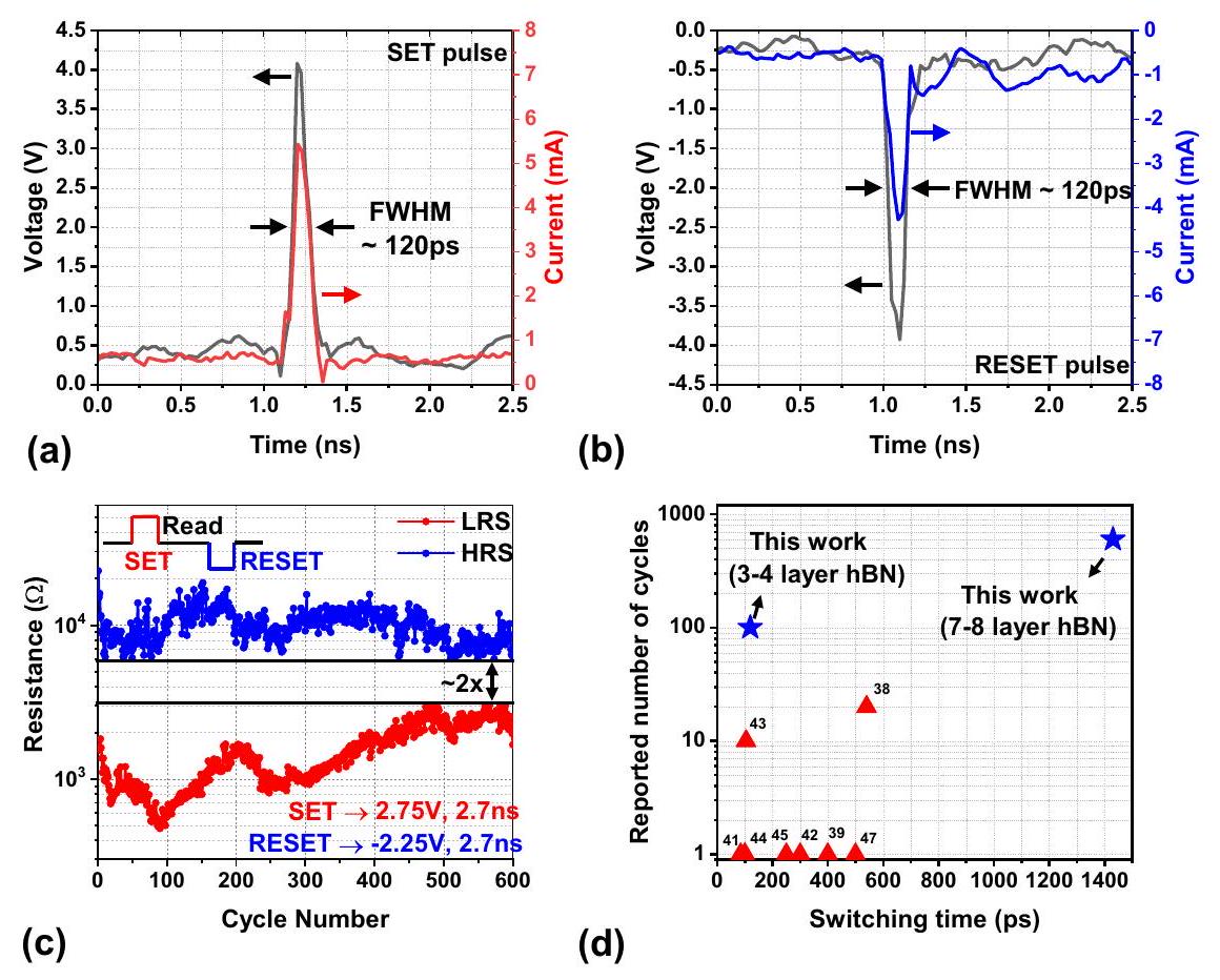
تظهر الجهاز 100 دورة متتالية من التبديل المتسق، وهو أعلى قدرة تحمل تم الإبلاغ عنها على الإطلاق باستخدام نبضات فائقة القصر. د رسم بياني يقارن أداء الأجهزة المقدمة في هذه المقالة مع ميمريستورات TMO و2D الأخرى.
خصائص التبديل العابرة بما في ذلك التأثيرات الثانوية مثل تسخين جول. بشكل عام، تكشف هذه الدراسة عن الإمكانات الحقيقية لميمريستورات المواد ثنائية الأبعاد لتطبيقات الحوسبة عالية السرعة، والتخزين، وRF المستقبلية.

طرق

تحضير نيتريد البورون السداسي

تم زراعة عدد قليل من طبقات hBN بواسطة ترسيب البخار الكيميائي (CVD) على رقائق النحاس المتاحة تجارياً (بسمك 25 ميكرومتر، نقاء 99.8%، معالجة حرارياً، غير مطلية – شركة ألفا أيسر). تم تلميع الرقائق كهربائياً باستخدام محلول قائم على حمض الفوسفوريك لتقليل خشونة السطح والقضاء على الخطوط النموذجية لرقائق النحاس المنتجة تجارياً. تم طي رقائق النحاس في حاوية ووضعها في وسط أنبوب الكوارتز. تم رفع درجة حرارة الفرن وتم معالجة الركائز حرارياً عند 1030 درجة مئوية لمدة 25 دقيقة في البيئة (معدل تدفق 30 SCCM). بعد معالجة الركائز بالتسخين، تم تسخين سلفيد الأمونيا-البوران (الموضوع في منطقة تسخين منفصلة – انظر الشكل التوضيحي 1) إلى 92-95 درجة مئوية في حمام مائي. عند هذه الدرجة، يتحلل سلفيد الأمونيا-البوران إلى بورازين، وأمينوبوران أحادي الجزيء، وهيدروجين يتم إدخاله إلى الحجرة من خلال غاز الحامل. تقوم الأنواع الكيميائية الماصة على سطح النحاس بتخليق طبقات hBN القليلة المرغوبة. خلال عملية النمو، معدل التدفق كان ووصل الضغط الكلي للحجرة إلى . كانت مدة النمو تتراوح بين 10 إلى 12 دقيقة. بعد النمو، تم تبريد الغرفة بسرعة ( ) من خلال عملية تبريد طبيعية وتم الحفاظ على تدفق الغاز طوال عملية التبريد. تم تأكيد الهيكل الطبقي لأفلام hBN المزروعة باستخدام تصوير TEM (الشكل 1 والأشكال التكميلية 2، 3).

نقل فيلم hBN

تم نقل أفلام hBN الناضجة من رقائق النحاس إلى Si/ ركيزة لتصنيع الأجهزة. لتمكين
عملية النقل، تم طلاء رقائق النحاس مع أفلام hBN باستخدام تقنية الطلاء الدوراني بـ PMMA (بولي ميثيل ميثاكريلات) بسرعة 3000 دورة في الدقيقة لمدة دقيقة واحدة، تلاها خبز عند 180 درجة مئوية لمدة دقيقة واحدة. يوفر طبقة PMMA الدعم والحماية لأفلام hBN خلال عملية النقل. تم نقل أفلام hBN باستخدام طريقة النقل الفقاعي باستخدام محلول NaOH كالإلكتروليت. تم استخدام رقائق النحاس المطلية بالطرد المركزي كالكاثود وتم استخدام ركيزة النيكل كالأندود لعملية التحليل الكهربائي. تطبيق 1.8 فولت على الأندود يولد فقاعات الغاز عند الكاثود مما يؤدي إلى فصل hBN عن ورقة النحاس. تم شطف مجموعة hBN/PMMA المنفصلة عدة مرات لإزالة الرواسب التي تم إدخالها أثناء عملية النقل وتم جمعها على الركيزة المستهدفة مع القطب السفلي المنقوش. تم تخزين العينة مع مجموعة hBN/PMMA في غرفة فراغ طوال الليل لإزالة أي فقاعات ماء محاصرة بين فيلم hBN والركيزة. ثم تم إزالة PMMA عن طريق ترك العينة في الأسيتون لمدة ساعتين. لإزالة أي رواسب PMMA إضافية، تم تسخين العينة عند 200 درجة مئوية لمدة 4 ساعات في غرفة فراغ عالية (1e-6 Torr). تم تأكيد النقل الناجح لفيلم hBN إلى الركيزة المستهدفة بواسطة مطيافية رامان وXPS، وتصوير SEM وTEM (الأشكال التكميلية 2،3،4).

تصنيع جهاز الميمريستور

يتضمن تصنيع جهاز الميمريستور تشكيل القطب السفلي (BE) باستخدام الطباعة الحجرية بالأشعة الإلكترونية على المواد الأساسية، تليها تبخر الإلكترونيات المعدنية تم نقل فيلم hBN المزروع إلى BE باستخدام طريقة النقل بالفقاعات المدعومة بـ PMMA. اكتمل تصنيع الجهاز من خلال تشكيل وترسيب معدن القطب العلوي (TE). بحيث يكون معدن التيتانيوم في اتصال مباشر مع hBN. الأجهزة المصنعة لها مساحة مقطع عرضي متغيرة بين و تم تأكيد الهيكل النهائي للجهاز باستخدام التصوير البصري وتصوير المجهر الإلكتروني الماسح (الشكل التوضيحي 6).

توصيف التيار المستمر الكهربائي

تم إجراء توصيف التيار المستمر (الشكل 2a-d) للذاكرات المصنوعة باستخدام محطة اختبار (Cascade Microtech) ومحلل معلمات أشباه الموصلات (Agilent 4156 C). في جميع القياسات، تم تطبيق الجهد على القطب العلوي مع تأريض القطب السفلي، وعادة ما تم ضبط الحد الأقصى للتيار على 100 ميكروأمبير. تم إجراء قياسات درجة الحرارة (الشكل 2e, f) في محطة اختبار مبردة (Lakeshore FWP6) متصلة بمحلل معلمات أشباه الموصلات Agilent B1500.

توصيف النبض الكهربائي

تم إجراء توصيف النبضات (الأشكال 3، 4، 5، 6) للذاكرات الموصلة في إعداد قياس تردد الراديو المخصص داخل الشركة. تم استخدام نبضات نانوثانية ( تم توليدها باستخدام مولد نبضات Picosecond Pulse Labs 10070A. تم توصيل هذه النبضات الفائقة القصر إلى الميمريستورز عبر مقاومة ( ) شبكة متطابقة للقضاء على الانعكاسات (انظر الشكل التكميلي 12). أ تم لحام مقاوم إنهاء على طرف المجس لضمان أقصى نقل للطاقة إلى الجهاز بالإضافة إلى توفير مسار سريع لتفريغ الشحنات الطفيلية. تم مراقبة نبضة الجهد المرسلة إلى الجهاز من خلال مقسم إشارة يقوم بأخذ عينة من الإشارة مع تخفيض قدره 20 ديسيبل. تؤدي نبضة الجهد إلى تحفيز نبضة تيار تنتقل إلى أسفل نحو جهاز الأوسيلوسكوب. هنا تم تقسيم الإشارة إلى مكونات تيار متردد وتيار مستمر باستخدام مقسم انحياز. تم التقاط المكون المتردد من الإشارة باستخدام أوسيلوسكوب عالي الأداء (Agilent DSA91304A-13 GHz، 40GSa/s). نظرًا لأن مقاومة الإدخال لجهاز الأوسيلوسكوب هي فقط الإشارات الحالية ذات السعة يمكن التقاطها بشكل موثوق. ومع ذلك، فإن الميمريستور عادةً ما يوصل تيارًا يتراوح بين 1 ميكروأمبير إلى 100 ميكروأمبير تحت فولتية القراءة ( ). لذلك، لدراسة تبديل الميمريستور، تم تضخيم المكون المستمر للإشارة باستخدام محول تيار إلى جهد (Femto DHCPA-100) بتردد تشغيل أقصى يبلغ 200 ميجاهرتز. تم مراقبة التبديل في الميمريستور من خلال أخذ عينات من البيانات المستمرة قبل (500 نانوثانية) وبعد (4 ميكروثانية) النبضة. يسمح تقسيم الإشارة بدراسة ديناميات الميمريستور أثناء التبديل (الأشكال 3، 4أ، ب، هـ، و، 5ب، هـ) وكذلك بعد اكتمال التبديل (الأشكال 4ج، ز، ح، 5د، ف، 6ج). النبضة فائقة السرعة ( تم توليدها عن طريق إرسال نبضات نانو ثانية من خلال مولد مشط يعتمد على صمام استرداد خطوة.

الخصائص الفيزيائية

تم تأكيد جودة أفلام hBN المُركبة بواسطة مطياف رامان (ليزر 532 نانومتر – مطياف رامان رينيشاو InVia) ومطياف الأشعة السينية للألكترونات (XPS). تم توصيف الطوبوغرافيا السطحية لطبقات hBN المنقولة بواسطة المجهر الذري (Bruker Icon AFM). تم تصوير هيكل الجهاز النهائي باستخدام المجهر الضوئي، والمجهر الإلكتروني الماسح (Zeiss Neon 40 SEM) والمجهر الإلكتروني الناقل (Jeol neoARM Scanning TEM). تم إعداد مقطع عينة TEM باستخدام شعاع أيوني مركّز (Thermo Scientific Scios 2 HiVac).

توفر البيانات

يعلن المؤلفون أن البيانات التي تدعم نتائج هذه الدراسة متاحة ضمن المقالة وملفات المعلومات التكميلية الخاصة بها. جميع البيانات الأخرى ذات الصلة متاحة من المؤلف المراسل عند الطلب.

References

  1. Talib, M. A., Majzoub, S., Nasir, Q. & Jamal, D. A systematic literature review on hardware implementation of artificial intelligence algorithms. J. Supercomput. 77, 1897-1938 (2021).
  2. Capra, M. et al. An updated survey of efficient hardware architectures for accelerating deep convolutional neural networks. Future Internet 12, 113 (2020).
  3. Stoica, I. et al. A Berkeley view of systems challenges for Preprint at https://arxiv.org/abs/1712.05855 (2017).
  4. Pereira, F., Correia, R., Pinho, P., Lopes, S. I. & Carvalho, N. B. Challenges in resource-constrained IoT devices: energy and communication as critical success factors for future IoT deployment. Sensors 20, 6420 (2020).
  5. Fan, X. et al. Flexible and wearable power sources for next-generation wearable electronics. Batteries Supercaps 3, 1262-1274 (2020).
  6. Compagnoni, C. M. et al. Reviewing the evolution of the NAND flash technology. Proc. IEEE 105, 1609-1633 (2017).
  7. Hemink, G. & Goda, A. (eds) in Semiconductor Memories and Systems 119-158 (Woodhead publishing, 2022).
  8. Chua, L. Memristor-the missing circuit element. IEEE Trans. Circuit Theory 18, 507-519 (1971).
  9. Strukov, D. B., Snider, G. S., Stewart, D. R. & Williams, R. S. The missing memristor found. Nature 453, 80-83 (2008).
  10. Yang, J. J. et al. Memristive switching mechanism for metal/oxide/ metal nanodevices. Nat. Nanotechnol. 3, 429-433 (2008).
  11. Luo, Q. et al. 8-Layers 3D vertical RRAM with excellent scalability towards storage class memory applications. In: 2017 IEEE International Electron Devices Meeting (IEDM) (ed Gendt, S. D.) 2-7 (IEEE, 2017).
  12. Luo, Q. et al. Demonstration of 3D vertical RRAM with ultra lowleakage, high-selectivity and self-compliance memory cells. In: 2015 IEEE International Electron Devices Meeting (IEDM) (ed Suehle, J.) 10-12 (IEEE, 2015).
  13. Xu, X. et al. Fully CMOS compatible 3D vertical RRAM with selfaligned self-selective cell enabling sub- 5 nm scaling. In: 2016 IEEE Symposium on VLSI Technology (ed Philip Wong, H. S.) 1-2 (IEEE, 2016).
  14. lelmini, D. & Wong, H. S. P. In-memory computing with resistive switching devices. Nat. Electron. 1, 333-343 (2018).
  15. Yin, S., Sun, X., Yu, S. & Seo, J. S. High-throughput in-memory computing for binary deep neural networks with monolithically integrated RRAM and 90-nm CMOS. IEEE Trans. Electron Devices 67, 4185-4192 (2020).
  16. Pedretti, G. & lelmini, D. In-memory computing with resistive memory circuits: status and outlook. Electronics 10, 1063 (2021).
  17. Yin, S. et al. Monolithically integrated RRAM-and CMOS-based inmemory computing optimizations for efficient deep learning. IEEE Micro 39, 54-63 (2019).
  18. Kim, M. et al. Zero-static power radio-frequency switches based on MoS2 atomristors. Nat. Commun. 9, 1-7 (2018).
  19. Kim, M. et al. Non-volatile RF and mm-wave switches based on monolayer hBN. In: 2019 IEEE International Electron Devices Meeting (IEDM) (ed Datta, S.) 5-9 (IEEE, 2019).
  20. Kim, M., Pallecchi, E., Happy, H. & Akinwande, D. Single-Pole-Double-Throw RF switches based on monolayer . In: 2021 Device Research Conference (DRC) (ed Chen, Z.) 1-2 (IEEE, 2021).
  21. Wong, H. S. P. et al. Metal-oxide RRAM. Proc. IEEE 100, 1951-1970 (2012).
  22. Sawa, A. Resistive switching in transition metal oxides. Mater. Today 11, 28-36 (2008).
  23. Khan, R. et al. Oxide-based resistive switching-based devices: fabrication, influence parameters and applications. J. Mater. Chem. C 9, 15755-15788 (2021).
  24. Carlos, E., Branquinho, R., Martins, R., Kiazadeh, A. & Fortunato, E. Recent progress in solution-based metal oxide resistive switching devices. Adv. Mater. 33, 2004328 (2021).
  25. Jang, J., Pan, F., Braam, K. & Subramanian, V. Resistance switching characteristics of solid electrolyte chalcogenide Ag2Se nanoparticles for flexible nonvolatile memory applications. Adv. Mater. 24, 3573-3576 (2012).
  26. Pradel, A., Frolet, N., Ramonda, M., Piarristeguy, A. & Ribes, M. Bipolar resistance switching in chalcogenide materials. Phys. Status Solidi (a) 208, 2303-2308 (2011).
  27. Gao, S., Yi, X., Shang, J., Liu, G. & Li, R. W. Organic and hybrid resistive switching materials and devices. Chem. Soc. Rev. 48, 1531-1565 (2019).
  28. Yuan, L., Liu, S., Chen, W., Fan, F. & Liu, G. Organic memory and memristors: from mechanisms, materials to devices. Adv. Electron. Mater. 7, 2100432 (2021).
  29. Park, S. P. et al. Analysis of the bipolar resistive switching behavior of a biocompatible glucose film for resistive random access memory. Adv. Mater. 30, 1800722 (2018).
  30. Yang, Y. et al. Electrochemical dynamics of nanoscale metallic inclusions in dielectrics. Nat. Commun. 5, 4232 (2014).
  31. Yang, Y. et al. Observation of conducting filament growth in nanoscale resistive memories. Nat. Commun. 3, 732 (2012).
  32. Qian, F. et al. A leaky integrate-and-fire neuron based on hexagonal boron nitride (h-BN) monocrystalline memristor. IEEE Trans. Electron Devices 69, 6049-6056 (2022).
  33. Clima, S. et al. First-principles thermodynamics and defect kinetics guidelines for engineering a tailored RRAM device. J. Appl. Phys. 119 (2016).
  34. Yu, S., Guan, X. & Wong, H.S.P. On the stochastic nature of resistive switching in metal oxide RRAM: physical modeling, Monte Carlo simulation, and experimental characterization. In: 2011 International Electron Devices Meeting (ed Ishimaru, K.) 17-3 (IEEE, 2011).
  35. Jain, P. et al. 13.2 A embedded non-volatile ReRAM macro in 22nm FinFET technology with adaptive forming/ set/reset schemes yielding down to 0.5 V with sensing time of 5 ns at 0.7 V . In: 2019 IEEE International Solid-State Circuits Conference(ISSCC) (ed Spiegel, J. V. D.) 212-214 (IEEE, 2019).
  36. Liu, T.Y. et al. A 130.7 mm 2 2-layer 32Gb ReRAM memory device in 24nm technology. In: 2013 IEEE International Solid-State Circuits Conference Digest of Technical Papers (ed Nauta, B.) (San Francisco, CA, 2013).
  37. Chang, M. F. et al. 19.4 embedded 1 Mb ReRAM in 28 nm CMOS with 0.27-to-1V read using swing-sample-and-couple sense amplifier and self-boost-write-termination scheme. In: 2014 IEEE International Solid-State Circuits Conference Digest of Technical Papers (ISSCC) (ed Stetzler, T.) 332-333 (IEEE, 2014).
  38. Chen, Z. et al. Ultrafast multilevel switching in Au/YIG/n-Si RRAM. Adv. Electron. Mater. 5, 1800418 (2019).
  39. Wang, C. et al. Ultrafast RESET analysis of HfOx-based RRAM by sub-nanosecond pulses. Adv. Electron. Mater. 3, 1700263 (2017).
  40. Shrestha, P. R. et al. Energy control paradigm for compliance-free reliable operation of RRAM. In: 2014 IEEE International Reliability Physics Symposium MY-10 (IEEE, 2014).
  41. Choi, B. J. et al. High-speed and low-energy nitride memristors. Adv. Funct. Mater. 26, 5290-5296 (2016).
  42. Lee, H. Y. et al. Evidence and solution of over-RESET problem for HfO x based resistive memory with sub-ns switching speed and high endurance. In: 2010 International Electron Devices Meeting (ed leong, M.) 19-7 (IEEE, 2010).
  43. Choi, B. J. et al. Electrical performance and scalability of Pt dispersed nanometallic resistance switch. Nano letters 13, 3213-3217 (2013).
  44. Torrezan, A. C., Strachan, J. P., Medeiros-Ribeiro, G. & Williams, R. S. Sub-nanosecond switching of a tantalum oxide memristor. Nanotechnology 22, 485203 (2011).
  45. Böttger, U. et al. Picosecond multilevel resistive switching in tantalum oxide thin films. Sci. Rep. 10, 1-9 (2020).
  46. Zhang, F. et al. An ultra-fast multi-level MoTe 2-based RRAM. In: 2018 IEEE International Electron Devices Meeting (IEDM) (ed Takayanagi, M.) 22-27 (IEEE, 2018).
  47. Kim, M. et al. Monolayer molybdenum disulfide switches for 6 G communication systems. Nat. Electron. 5, 1-7 (2022).
  48. Chen, S. et al. Wafer-scale integration of two-dimensional materials in high-density memristive crossbar arrays for artificial neural networks. Nat. Electron. 3, 638-645 (2020).
  49. Zhu, K. et al. Graphene-boron nitride-graphene cross-point memristors with three stable resistive states. ACS Appl. Mater. Interfaces 11, 37999-38005 (2019).
  50. Zhuang, P. et al. Nonpolar resistive switching of multilayer-hBNbased memories. Adv. Electron. Mater. 6, 1900979 (2020).
  51. Fantini, A. et al. Intrinsic switching variability in HfO 2 RRAM. In: 2013 5th IEEE International Memory Workshop 30-33 (IEEE, 2013).
  52. Ambrogio, S. et al. Understanding switching variability and random telegraph noise in resistive RAM. In: 2013 IEEE International Electron Devices Meeting (ed Ghani, T.) 31-35 (IEEE, 2013)
  53. Guan, X., Yu, S. & Wong, H.S.P. On the switching parameter variation of metal-oxide RRAM-Part I: Physical modeling and simulation methodology. IEEE Trans. Electron Devices 59, 172-1182 (2012).
  54. Shen, Y. et al. Variability and yield in h-BN-based memristive circuits: the role of each type of defect. Adv. Mater. 33, 2103656 (2021).
  55. Shi, Y. et al. Electronic synapses made of layered two-dimensional materials. Nat. Electron. 1, 458-465 (2018).
  56. Lim, E. W. & Ismail, R. Conduction mechanism of valence change resistive switching memory: a survey. Electronics 4, 586-613 (2015).
  57. Chakraborty, I., Panwar, N., Khanna, A. & Ganguly, U. Space Charge Limited Current with Self-heating in based RRAM. Preprint at https://arxiv.org/abs/1605.08755 (2016).
  58. Puglisi, F. M. et al. 2D h-BN based RRAM devices. In: 2016 IEEE International Electron Devices Meeting (IEDM) (ed Fay, P.) 34-38 (IEEE, 2016).
  59. Zhu, K. et al. Hybrid 2D-CMOS microchips for memristive applications. Nature 618, 57-62 (2023).
  60. Yu, S. & Wong, H. S. P. Compact modeling of conducting-bridge random-access memory (CBRAM). IEEE Trans. Electron Devices 58, 1352-1360 (2011).
  61. Ielmini, D. Modeling the universal set/reset characteristics of bipolar RRAM by field-and temperature-driven filament growth. IEEE Trans. Electron Devices 58, 4309-4317 (2011).
  62. Huang, P. et al. A physics-based compact model of metal-oxidebased RRAM DC and AC operations. IEEE Trans. Electron Devices 60, 4090-4097 (2013).
  63. Ielmini, D., Nardi, F. & Cagli, C. Physical models of size-dependent nanofilament formation and rupture in NiO resistive switching memories. Nanotechnology 22, 254022 (2011).
  64. Jo, I. et al. Thermal conductivity and phonon transport in suspended few-layer hexagonal boron nitride. Nano Lett. 13, 550-554 (2013).
  65. Alam, M. T., Bresnehan, M. S., Robinson, J. A. & Haque, M. A. Thermal conductivity of ultra-thin chemical vapor deposited hexagonal boron nitride films. Appl. Phys. Lett. 104 (2014).
  66. Panzer, M. A. et al. Thermal properties of ultrathin hafnium oxide gate dielectric films. IEEE Electron Device Lett. 30, 1269-1271 (2009).
  67. Cappella, A. et al. High temperature thermal conductivity of amorphous thin films grown by low temperature ALD. Adv. Eng. Mater. 15, 1046-1050 (2013).
  68. Landon, C. D. et al. Thermal transport in tantalum oxide films for memristive applications. Appl. Phys. Lett. 107 (2015).
  69. Kwon, D. H. et al. Atomic structure of conducting nanofilaments in TiO2 resistive switching memory. Nat. Nanotechnol. 5, 148-153 (2010).
  70. Tsuruoka, T., Hasegawa, T., Terabe, K. & Aono, M. Conductance quantization and synaptic behavior in a Ta2O5-based atomic switch. Nanotechnology 23, 435705 (2012).
  71. Lee, S., Sohn, J., Jiang, Z., Chen, H. Y. & Philip Wong, H. S. Metal oxide-resistive memory using graphene-edge electrodes. Nat. Commun. 6, 1-7 (2015).
  72. Zhuang, P., Ma, W., Liu, J., Cai, W. & Lin, W. Progressive RESET induced by Joule heating in hBN RRAMs. Appl. Phys. Lett. 118, 143101 (2021).
  73. Lanza, M. et al. Temperature of conductive nanofilaments in hexagonal boron nitride based memristors showing threshold resistive switching. Adv. Electron. Mater. 8, 2100580 (2022).
  74. Li, S. et al. Fully coupled multiphysics simulation of crosstalk effect in bipolar resistive random access memory. IEEE Trans. Electron Devices 64, 3647-3653 (2017).
  75. Hsieh, C. C., Roy, A., Chang, Y. F., Shahrjerdi, D. & Banerjee, S. K. A sub-1-volt analog metal oxide memristive-based synaptic device with large conductance change for energy-efficient spike-based computing systems. Appl. Phys. Lett. 109, 223501 (2016).

شكر وتقدير

تم تنفيذ هذا العمل جزئيًا في مركز أبحاث الميكروإلكترونيات بجامعة تكساس، وهو عضو في البنية التحتية المنسقة للتكنولوجيا النانوية الوطنية (NNCI)، المدعومة من مؤسسة العلوم الوطنية (منحة ECCS-2025227). يشكر A.R. الدعم من مجلس أبحاث العلوم والهندسة، حكومة الهند، منحة #SRG/2022/000788. وقد تم دعمه جزئيًا من قبل منحة شركة أبحاث أشباه الموصلات LMD 3009.001.

مساهمات المؤلفين

S.S.T.N. و A.R. و S.K.B. تصوروا هذا العمل وأعدوا المخطوطة. S.S.T.N. قام بتخليق المادة ثنائية الأبعاد، وصنع الميمريستور وأجرى التوصيف الكهربائي. A.R. أجرى قياس طيف الأشعة السينية. S.S.T.N. و D.V. و G.B. أعدوا إعداد قياس النبضات الفائقة السرعة وساعدوا في تحليل بيانات القياس. M.C. و K.C.M. و J.W. قاموا بتصوير المجهر الإلكتروني الناقل للأجهزة المصنعة. S.S.T.N. و M.D. أجروا قياس المقاومة بناءً على درجة الحرارة للأجهزة المصنعة. S.S.T.N. و A.R. و A. و J.V.S و J.P.K. شاركوا في تحليل نتائج القياس من خلال النموذج الكهربائي الحراري، والنموذج الظاهري والمحاكاة الحرارية. I.R.G.D. أجرى تجربة AFM الموصل وحلل النتيجة. جميع المؤلفين ناقشوا وساهموا في التحليل المقدم في المخطوطة. S.K.B. أشرف على الدراسة.

المصالح المتنافسة

يعلن المؤلفون عدم وجود مصالح متنافسة.

معلومات إضافية

معلومات إضافية النسخة الإلكترونية تحتوي على
المواد التكميلية المتاحة على
https://doi.org/10.1038/s41467-024-46372-y.
يجب توجيه المراسلات والطلبات للحصول على المواد إلى S. S. Teja Nibhanupudi أو Anupam Roy أو Sanjay K. Banerjee.
معلومات مراجعة الأقران تشكر Nature Communications ماريو لانزا وماجد محسني والمراجعين المجهولين الآخرين على مساهمتهم في مراجعة الأقران لهذا العمل. يتوفر ملف مراجعة الأقران.
معلومات النسخ والتصاريح متاحة على
http://www.nature.com/reprints
ملاحظة الناشر تظل Springer Nature محايدة فيما يتعلق بالمطالبات القضائية في الخرائط المنشورة والانتماءات المؤسسية.
الوصول المفتوح هذه المقالة مرخصة بموجب رخصة المشاع الإبداعي للاستخدام والمشاركة والتكيف والتوزيع وإعادة الإنتاج في أي وسيلة أو صيغة، طالما أنك تعطي الائتمان المناسب للمؤلفين الأصليين والمصدر، وتوفر رابطًا لرخصة المشاع الإبداعي، وتوضح ما إذا تم إجراء تغييرات. الصور أو المواد الأخرى من طرف ثالث في هذه المقالة مشمولة في رخصة المشاع الإبداعي للمقالة، ما لم يُشار إلى خلاف ذلك في سطر الائتمان للمادة. إذا لم تكن المادة مشمولة في رخصة المشاع الإبداعي للمقالة وكان استخدامك المقصود غير مسموح به بموجب اللوائح القانونية أو يتجاوز الاستخدام المسموح به، ستحتاج إلى الحصول على إذن مباشرة من صاحب حقوق الطبع والنشر. لعرض نسخة من هذه الرخصة، قم بزيارةhttp://creativecommons.org/licenses/by/4.0/.
(ج) المؤلفون 2024

  1. مركز أبحاث الميكروإلكترونيات، جامعة تكساس في أوستن، أوستن، تكساس 78758، الولايات المتحدة الأمريكية. معهد بيرلا للتكنولوجيا، ميسرا، رانشي 835215، الهند. مختبرات HRL، ماليبو، كاليفورنيا 90265، الولايات المتحدة الأمريكية. معهد مواد تكساس، جامعة تكساس في أوستن، أوستن، تكساس 78712، الولايات المتحدة الأمريكية. حلول M2D، أوستن، تكساس 78758، الولايات المتحدة الأمريكية. البريد الإلكتروني: subrahmanya_teja@utexas.edu; royanupam@bitmesra.ac.in; banerjee@ece.utexas.edu

Journal: Nature Communications, Volume: 15, Issue: 1
DOI: https://doi.org/10.1038/s41467-024-46372-y
PMID: https://pubmed.ncbi.nlm.nih.gov/38485722
Publication Date: 2024-03-14

Ultra-fast switching memristors based on two-dimensional materials

Received: 9 March 2023
Accepted: 26 February 2024
Published online: 14 March 2024
(D) Check for updates

S. S. Teja Nibhanupudi © , Anupam Roy (B) , Dmitry Veksler , Matthew Coupin © , Kevin C. Matthews © , Matthew Disiena , Ansh¹, Jatin V. Singh © , loana R. Gearba-Dolocan , Jamie Warner , Jaydeep P. Kulkarni’, Gennadi Bersuker & Sanjay K. Banerjee

Abstract

The ability to scale two-dimensional (2D) material thickness down to a single monolayer presents a promising opportunity to realize high-speed energyefficient memristors. Here, we report an ultra-fast memristor fabricated using atomically thin sheets of 2D hexagonal Boron Nitride, exhibiting the shortest observed switching speed ( 120 ps ) among 2D memristors and low switching energy (2pJ). Furthermore, we study the switching dynamics of these memristors using ultra-short ( ) voltage pulses, a frequency range that is highly relevant in the context of modern complementary metal oxide semiconductor (CMOS) circuits. We employ statistical analysis of transient characteristics to gain insights into the memristor switching mechanism. Cycling endurance data confirms the ultra-fast switching capability of these memristors, making them attractive for next generation computing, storage, and Radio-Frequency (RF) circuit applications.

In today’s digital era, the role of memory technology has become integral, particularly in the context of artificial intelligence (AI) applications. Several AI tasks, such as classification, recognition, natural language processing, prediction etc., heavily rely on large-scale memory storage and processing capability of the underlying hardware . Conventional memory technologies like Static Random Access Memory (SRAM) or Dynamic Random Access Memory (DRAM) are energy-inefficient for implementing these data-intensive applications due to their volatile nature, resulting in dynamic as well as static power dissipation. These energy requirements are even more stringent for battery-operated mobile, wearable electronics, and Internet of Things (IoT) edge devices . Although flash memory is non-volatile, the slow programming speed ( us) makes it impractical for these applications . To effectively harness and maximize the potential of AI and other emerging applications, an ultra-fast non-volatile memory is necessary.
Memristors are promising devices in the emerging non-volatile memory landscape that have shown great potential owing to their small footprint ( ), fast operation, and low power consumption .
Several studies explored the use case of memristors for storage, memory-centric computing , and high-frequency RF applications . In the past decade, memristors fabricated using a variety of materials such as Transition Metal Oxides (TMO) , chalcogenides , and organic materials have been extensively studied. TEM studies have conclusively established that the resistive switching in memristors can be attributed to the presence of conductive nanofilaments . Based on the experimental observations, the switching dynamics in memristors have been captured using different modeling techniques . The commercially available memristors typically switch in range, making them slower than state-of-the-art DRAM . Although a few studies have reported fasterswitching memristors ( , the fast-switching dynamics have not been thoroughly studied.
Here, we present an ultra-fast memristor fabricated using a twodimensional (2D) material, i.e., hexagonal Boron Nitride (hBN) as the switching layer . The atomically thin nature of the 2D material facilitates rapid filament dynamics enabling an ultra-fast and energyefficient memristor. We study these memristors using ultra-short
pulses ( ) in a custom-built RF test setup. Moreover, since the filament formation/dissolution in memristors is a stochastic process , we employ statistical analysis of the transient switching characteristics to study these memristors. Statistical data provided critical insights into the switching mechanism and the inherent stochasticity of the filament dynamics. To the best of our knowledge, this is the first study of this kind not just in 2D memristors but among the plethora of scientific reports based on TMO memristors. In addition, by leveraging cues from statistical data, we model the fast-switching dynamics using a combination of finite element-based physics solver, empirical, and analytical equations.

Results

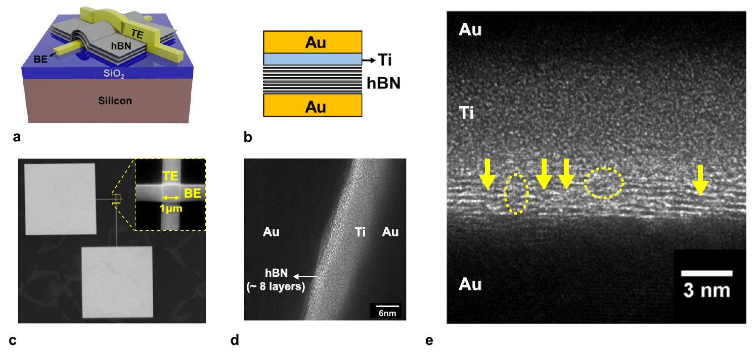
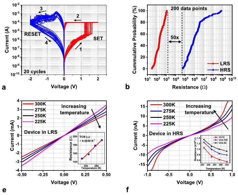
Device fabrication and DC electrical performance

Structural features of the fabricated memristor with few-layer hBN sandwiched between active ( Ti ) and inert ( Au ) electrodes are shown in Fig. 1a, b. The switching hBN layers were synthesized using chemical vapor deposition (CVD) on copper foil and transferred onto substrate for device fabrication (see Supplementary Fig. 1 and Methods section for details). The final device structure was confirmed using scanning electron microscopy (SEM) (Fig. 1c) and cross-sectional transmission electron microscopy (TEM) (Fig. 1d) images. Synthesized hBN films are 7-8 layers thick with an inter-layer spacing of 0.33 nm , as evident from the TEM images (Supplementary Fig. 2,3). These CVDgrown films contain single atom and few atom-wide intrinsic defects, as seen in Fig. 1e. These defects facilitate the formation of conductive filaments, which, in turn, enable the desired resistive switching behavior. Notably, previous studies have reported the absence of a resistive switching phenomenon in exfoliated flakes that lack intrinsic defects . The crystal structure and chemical composition of the synthesized hBN films were corroborated using Raman and X-ray photoelectron spectroscopy (XPS) techniques (Supplementary Fig. 4). In addition, memristors fabricated with thinner ( layers) hBN films (Supplementary Fig. 5), synthesized by tuning the growth parameters were studied for comparison.
Devices with different cross-sectional areas varying from to were fabricated (Supplementary Fig. 6) and characterized. The majority of as-fabricated (virgin) devices ( ) exhibit high resistance ( ), which indicates the excellent quality of the synthesized hBN films (Supplementary Fig. 7.1). The remaining
devices with low initial resistance likely contain grain boundaries or multi-atom wide defects which were probably introduced during the fabrication processes. These leaky devices were discarded and not considered for further analysis. The high voltage sweep applied to the Ti electrode during the forming process generates the conductive filament inside the memristor. Supplementary Fig. 7.2 shows that the magnitude of the forming voltage is directly correlated to the initial resistance of the memristor. Consequently, devices with higher initial resistance, characterized by fewer defects, require a higher voltage to establish the conductive filament. Apparently, this trend holds true for all devices, irrespective of the device cross-section. To ensure that the measured initial resistance and subsequent resistive switching were not influenced by an unintentional layer at the interface ( Ti layer susceptible to oxidation), devices fabricated without the hBN layer were measured (Supplementary Fig. 8). These devices exhibit ohmic conduction with low resistance ( ), confirming the absence of any substantial layer.
After the forming operation, memristors exhibit bipolar resistive switching characteristics with positive voltage and negative voltage applied to the top Ti electrode for SET (transition to lower resistance) and RESET (transition to higher resistance) operations, respectively. Figure 2a shows the representative DC current-voltage ( ) sweeps of the memristor device with a current compliance limit of . Additional sweeps measured from multiple devices are presented in Supplementary Fig. 9. Data collected from 200 such traces were analyzed to quantify the variation in the device characteristics. Statistical analysis shows that the minimum separation between the highresistance state (HRS) and low-resistance state (LRS), is ~50x (Fig. 2b), considering variations. Similarly, the variations in the SET and RESET voltages are characterized by Gaussian distributions with mean values ( ) of 1.73 V and -0.85 V , respectively (Fig. 2c). The SET voltage distribution displays higher dispersion (standard deviation ( ) of 0.5 V ) mainly attributable to the device-to-device variations (see Supplementary Fig. 10 for discussion). In comparison, the RESET voltage distribution is rather tight with of 0.27 V . This variation in switching voltage can be further reduced by ensuring high crystalline quality of the synthesized 2D material and by employing superior device fabrication methods that can reduce electrode surface roughness.
To study the transport mechanisms responsible for the switching process, SET sweep was plotted on a log-log scale
Fig. 1 | Device structure of the fabricated 2D hBN memristor. a Schematic drawing of the memristor device. Cross-section schematic showing the metal contact used for top (titanium) and bottom electrodes (gold). c SEM image of the device after fabrication (inset) zoomed image where top and bottom electrodes
cross. d Phase contrast TEM image of the device cross-section showing 8 layer thick hBN sandwiched between metal electrodes. e Magnified TEM cross-section showing the layered structure of hBN with single-atom defects (arrows) and few atom wide amorphous regions (dashed circles).
Fig. 2 | DC characterization of the 2D hBN memristor. a DC sweeps of the hBN memristors shown for 20 consecutive cycles (SET curves shown in red traces and RESET curves shown in blue traces). Cumulative probability distribution of the resistance in HRS and LRS states extracted from DC sweeps at collected from traces. c SET/RESET voltage distribution using 100uA compliance current. d SET I-V curve plotted on log-log scale shows regions with varying slope in HRS and linear slope in LRS. e sweep of the device in LRS measured at various operating temperatures ( 225 K (pink curve), 250 K (black curve), 275 K (blue curve), 300 K (red curve)); (inset) resistance extracted at plotted vs.
temperature. The memristor in LRS has a positive temperature coefficient of resistance indicating the formation of metallic filaments ( ) sweeps of the device in HRS measured at various operating temperatures ( ); (inset) resistance extracted at (black curve), 0.75 V (blue curve), 1 V (red curve) plotted vs. temperature. Reducing resistance with increasing temperature suggests conduction through insulating medium. g TEM cross-section illustrating the locations where electron energy loss spectroscopy (EELS) profile was collected. Points A (red curve), D (black curve) are located inside Au electrode, point B (blue curve) is located inside hBN layer, and point C (green curve) inside Ti electrode.
(Fig. 2d). Device transitioning to LRS during SET traverses through conductance regions with varying slopes, indicating that the dominant charge transport mechanism varies: ohmic conduction with slope , space-charge limited conduction (SCLC) in regions with slope and trap-fill limited SCLC in regions with slope . Bidirectional voltage sweeps confirm that the change in slope is reversible and, therefore, not related to the filament formation (Supplementary Fig. 11). Further voltage increase results in an abrupt current jump (slope ) suggesting the formation of an ohmic conductive filament (slope ). The current compliance prevents further expansion of the filament and protects the device from thermal breakdown. To corroborate the filamentary conduction mechanism, conductive atomic force microscopy (CAFM) measurements were conducted on a stressed device. The CAFM maps reveal isolated regions exhibiting high current, clearly indicating the formation of conductive filaments across the hBN layer (details in Supplementary Fig. 12). Likewise, the RESET I-V sweep also exhibits ohmic conduction in LRS and SCLC in the HRS, as seen in Supplementary Fig. 11. To understand the fundamental nature of the filament, sweeps were measured at different operating temperatures. The resistance of the device in LRS increases with temperature suggesting the metallic nature of the filament (Fig. 2e). On the other hand, HRS resistance decreases with temperature indicating energy-activated conduction (Fig. 2f). In addition, Electron Energy Loss Spectroscopy (EELS) was employed to investigate the elemental composition of the filament. The EELS profiles gathered from four distinct points (A, B, C, D) on the TEM cross-section are plotted in Fig. 2 g . A prominent Ti peak was observed at point C (located inside the Ti layer) while a faint peak was observed at point B (located within hBN layers). The presence of Ti peak at location B suggests titanium ion migration into the hBN layer, which contributes to the filament formation. Similar observations of titanium ion-constituted filaments have been reported in previous studies . Overall, the temperature measurements and the EELS analysis collectively reinforce the existence of metallic filaments (composed of Ti atoms) in the 2D hBN memristor.

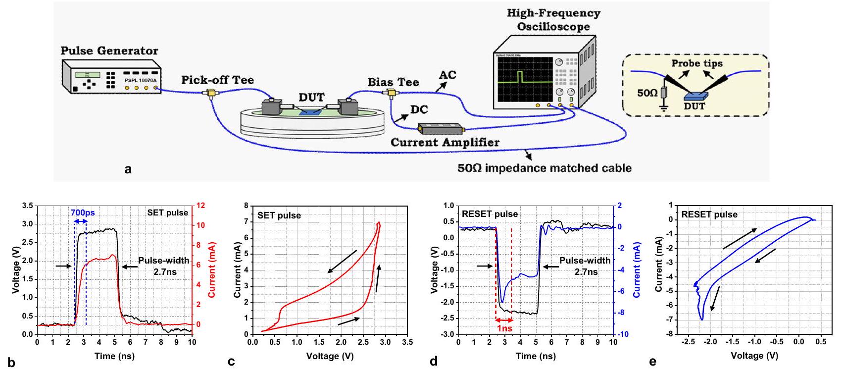
Pulse voltage stress operations

The switching dynamics of the memristors were studied by applying a sequence of ultra-short voltage pulses ( ) with a rise/fall time of . In our test setup, the voltage pulses were delivered to the device through an impedance ( ) matched network, as schematically illustrated in Fig. 3a (additional details provided in the Methods section). A termination resistor was soldered onto the probe-tip (Fig. 3a), which minimized reflections and ensured maximum power transfer to the device (Supplementary Fig. 13). The resistance state of the device was measured by applying a constant DC offset ( ) to the pulse. This DC component of the current signal was amplified and measured on the oscilloscope.
Figure 3b shows the oscilloscope waveforms of the applied voltage pulse and the measured current during a SET operation. The induced current rises slowly compared to the voltage pulse and saturates at which can be characterized as the SET switching time of the memristor. The characteristics extracted from the transient waveforms in Fig. 3b clearly demonstrate the resistive switching behavior (Fig. 3c). To verify that the memory window observed in Fig. 3c originates from memristor resistive switching and not from system parasitics, we apply similar voltage pulses to discrete resistors (Supplementary Fig. 14). Further, the successful SET operation was also confirmed through the DC read signal (Supplementary Fig. 15). Figure 3d shows the transient waveforms of the voltage and current pulses for the RESET operation. Initially, since the device is in LRS, the current increases, reaches a maximum, and gradually decreases as the filament dissolution proceeds. This initial current surge should not be confused with parasitic displacement current since the shunt resistor placed on the probe tip provides an effective path to dissipate parasitic charges. The successful resistive switching during the RESET operation is confirmed by the plot (Fig. 3e) and the DC read signal (Supplementary Fig. 15).

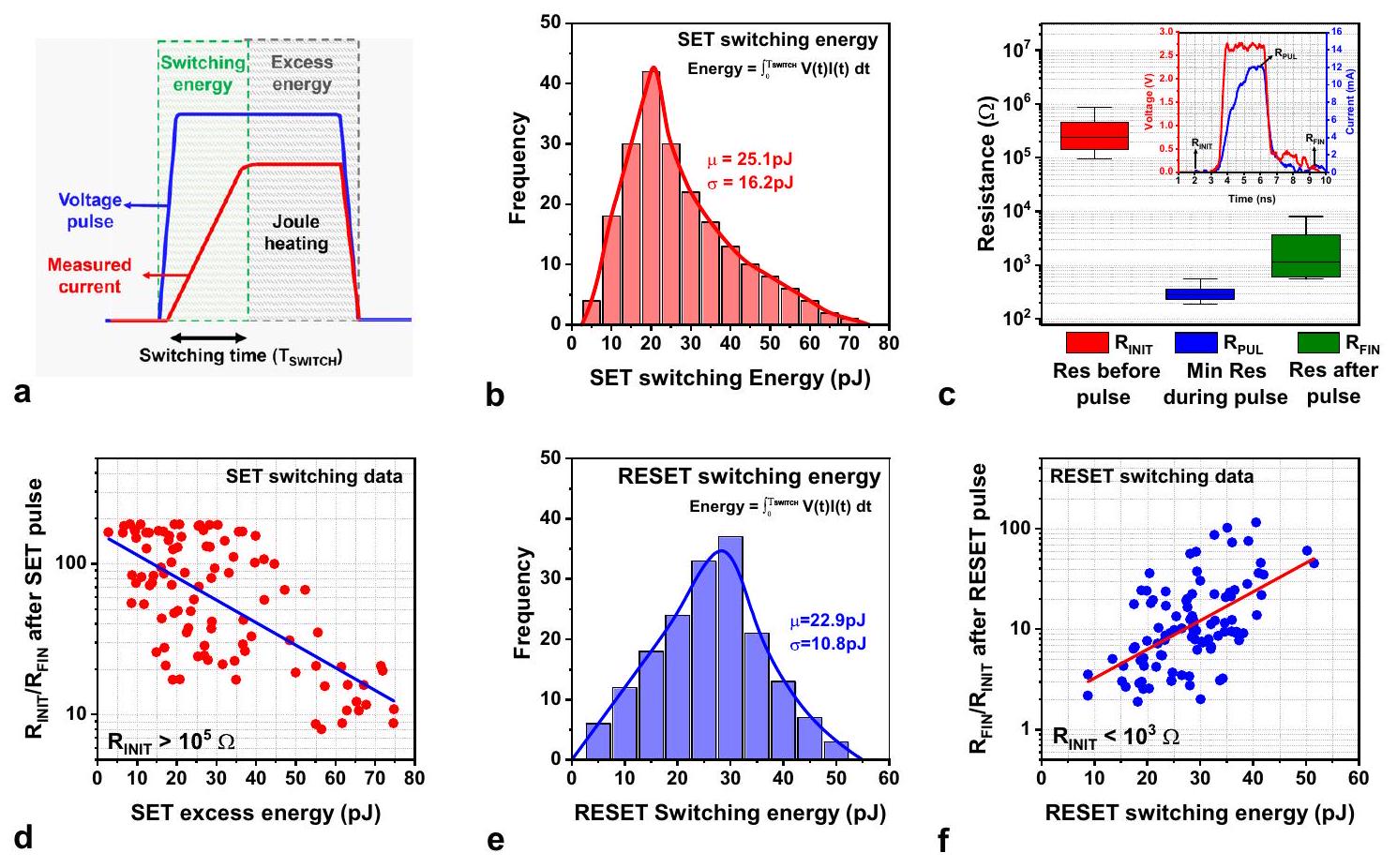
Statistical analysis of switching dynamics

The filament formation and dissolution are stochastic processes determined by several factors apart from the electric field, such as
energy generation/dissipation, defects in the 2D film, and the interface with the electrodes. Hence, statistical analysis of the switching dynamics was employed to gain insights into the resistive switching mechanism. This study was conducted by applying identical voltage pulses ( ) and analyzing changes in the switching behavior across different devices/cycles. Data from the measured current pulses display a wide range of intrinsic switching
times ( 600 ps to 2.5 ns-see Supplementary Fig. 16 for details) as seen from Fig. 4 a (voltage pulses traces omitted for clarity). The distribution of switching times (extracted from each current trace) has a mean value of 1.32 ns and a standard deviation of 670 ps (Fig. 4b). Notably, of the devices exhibit sub-nanosecond switching.
Further, to understand the effect of filament morphology on switching dynamics, we studied the correlation between switching
Fig. 3 | Ultra-fast pulse characterization setup and waveforms. a Schematic drawing of the high-frequency pulse test setup; (right) zoomed schematic of the probe tips with termination for maximum power transfer .b Applied voltage pulse (black trace) and measured current (red trace) waveform for SET operation. The applied pulse has a pulse-width of 2.7 ns and the device switches in about
plot of the data in (b) shows change in resistance during the applied pulse. d Applied voltage pulse (black trace) and measured current (blue trace) waveform for RESET operation (e) plot of the data in (d) shows change in resistance during the applied pulse.
Fig. 4 | Statistical analysis of transient switching characteristics using ultra-fast pulses. a Measured current waveforms on 30 different devices under identical applied voltage pulses ( ) during SET operation. b SET switching time distribution created from 200 measurements with a mean value of 1.32 ns . c Correlation between SET switching time and resulting relative change in resistance values. Large resistance change requires a longer switching time. d Transient response of average interface temperature for 2.5 nm thick hBN and 5 nm thick HfOx, obtained through COMSOL simulation (inset) snapshot of
time and resistance change induced by the SET pulse ( where is the initial state resistance and is the final state resistance) (Fig. 4c). Here, the resistance values ( ) were obtained by DC measurements before and after the SET pulse. For this study, devices were programmed (by leveraging the gradual RESET characteristics shown in Fig. 2a) such that the initial resistances were in the range and the set pulse results in . The switching time varies among devices even with the same and , highlighting the stochastic nature of filament growth. However, a clear upward trend indicates that larger resistance change (which entails more structural modifications) requires longer switching times.
The switching mechanism in 2D memristors is typically based on the formation and dissolution of conductive filaments . Although a recent study reports non-filamentary conduction in hBN memristors, our devices exhibit filamentary switching, as confirmed by the ohmic behavior in LRS and positive TCR in LRS. The filament growth in memristors proceeds through vertical propagation (around defects or weak spots), followed by lateral expansion . The current flowing through the initially formed narrow filament (single atom or few atoms wide) raises the temperature inside the memristor through the Joule heating phenomenon. The generated temperature helps the Ti ions surmount the energy barrier (Arrhenius dependence) and migrate into the hBN layer, further propelling the filament growth . To understand the fundamental factors responsible for the ultra-fast switching in 2D memristors, we conducted transient thermal analysis using a finite element method-based physics solver (COMSOL). The ultra-thin 2D hBN layer increases the electric field as well as the temperature in the memristor, both of which promote rapid filament growth. Moreover, the high in-plane thermal conductivity of the hBN layer ( higher than transition metal oxides ) rapidly spreads the heat generated in the filament (joule heating) to the Ti/hBN interface (detailed analysis presented in Supplementary Fig. 17). The high
temperature at the Ti/hBN interface facilitates Ti ion release from the electrode into the hBN switching layer. Figure 4d compares the average interface temperature for our devices and memristors with 5 nm thickness (typical thickness for oxide memristors). Evidently, the interface temperature rises rapidly in our devices compared to thicker oxide memristors, consequently resulting in faster resistive switching.
Similar to SET operation, RESET also displays a range of intrinsic switching times (Fig. 4e). The RESET operation is slower than the SET operation (distribution ns, ps) with only of the devices exhibiting sub-ns switching (Fig. 4f). As in SET, a larger resistance increase is associated with a longer switching time (Fig. 4 g ). Here, the devices have , and the RESET pulse results in . Further, the switching endurance test demonstrates one of the highest reported values (600 cycles) with the shortest applied pulses ( ) in 2D memristors (Fig. 4h). Consistent switching between resistance states is very promising since it demonstrates the potential of 2D memristors for ultra-fast switching memory applications.

Role of Joule heating on filament stability

Several studies have reported that Joule heating promotes filament dissolution in TMO memristors as well as in 2D memristors . Especially in devices with metallic filaments, large LRS current generates considerable heat ( ) that accelerates the outdiffusion of metal ions . The joule heating can be estimated by the energy generated inside the memristor, which can be calculated by integrating the product of transient voltage and current pulses (obtained from Fig. 4a, e) over time ( ) (see Supplementary Fig. 18 for details). This energy can be roughly segregated into switching energy and excess energy, as shown by the schematic in Fig. 5a. Switching energy contributes to the resistive switching process while excess energy continues to dissipate throughout the device after the switching process is complete. The switching energy driving the
Fig. 5 | Statistical analysis of memristor switching energy. a Schematic representation of the partition between switching energy and excess energy. SET switching energy distribution created from 200 measurements with a mean of 25.1 pJ . c Resistance distribution of (red box plot), (blue box plot), and (green boxplot) (inset) waveform illustrating the time instance at which the resistances were measured. The distribution clearly indicates the filament
resistance increases after pulse termination. d Relative resistance change after SET pulse variation vs excess energy expended in the device. Since excess energy is proportional to the Joule heating in the device, higher excess energy results in narrowing of the filament. e RESET switching energy distribution created from 175 measurements with a mean of 22.9 pJ. f Relative resistance change after RESET pulse vs switching energy.
SET operation has a mean of 25.1 pJ and a standard deviation of 16.2 pJ (Fig. 5b). On the other hand, the mean excess energy ( ) is higher than the switching energy attributable to the large LRS current flowing through the device.
For the SET transition, the memristor resistance distribution measured after the pulse was observed to be higher than the resistance during the pulse (Fig. 5c). Ideally, the resistance should have remained unchanged as the memristor in LRS exhibits linear ohmic conduction (based on Fig. 2d). Identical pulses applied to discrete resistors displayed no change in resistance during and after the pulse (Supplementary Fig. 19), confirming that the test setup parasitics do not contribute to the resistance change. We hypothesize that the joule heating-assisted filament narrowing is responsible for the observed resistance increase. To understand how this phenomenon affects the final resistance state ( ), the correlation between excess energy dissipated in the device (proportional to filament temperature) and the resistance change ( ) was studied (Fig. 5d). For this study, devices with similar initial resistance ( ) were chosen to eliminate the impact of initial filament morphology. Evidently, higher excess energy results in lower resistance change, indicating significant filament narrowing caused by enhanced joule heating. Supplementary Fig. 20 presents a further analysis of resistance change induced by Joule heating.
The phenomenological model based on the Arrhenius relationship is a widely accepted model which satisfactorily captures the filament growth dynamics in TMO memristors . Therefore, in this study, we employ a modified version of this model to capture the growth dynamics as well as the Joule heating-induced filament narrowing in our 2D memristors. In the classic model, time dependency of the filament growth is described by the Arrhenius relationship , where is the filament diameter and is the activation energy and accounts for the barrier lowering due to the applied voltage. This simple relationship cannot capture the filament narrowing observed in our devices. Therefore, an additional term was included that accounts for Joule heating-induced filament dissolution (see Supplementary Fig. 21 for detailed analysis). Based on this model, the following observations can be deduced: During the switching energy phase, when the Joule heating is insignificant (low current in the memristor), the filament growth rate dominates, resulting in filament expansion. On the other hand, during the excess energy phase when Joule heating is significant (high current in the memristor), the filament growth rate balances the filament dissolution rate resulting in current saturation. Finally, during the voltage pulse falling transition, the filament growth rate (determined by ) decreases faster than filament dissolution rate (determined only by ), thereby resulting in narrowing of the filament. A self-consistent electro-thermal solver using the proposed model clearly captures the filament narrowing phenomenon (see Supplementary Fig. 21) which closely matches with the experimental data presented in Fig. 5c. In addition to the proposed electro-thermal model, the resistance evolution of the memristor can be adequately captured through a simple empirical model. The Arrhenius relationship with an added filament enlargement factor produces a good fit to measured data (Supplementary Fig. 22). In this model, the temperature is considered constant, which significantly reduces the computational cost. Such models are particularly beneficial for implementing large circuits using the SPICE simulator.
Mean RESET switching energy ( ) is slightly lower than the SET switching energy, as seen from Fig. 5e. Unlike SET operation, Joule heating in the RESET operation is dominant during the switching energy phase (wider filaments supporting higher currents). The resistance change ( ) after the RESET pulse clearly increases with increasing switching energy, as seen in Fig. 5f. A similar trend of increasing resistance change can be observed from the total energy plots presented in Supplementary Fig. 23. Further, to confirm the role of heat on filament stability, we conducted retention studies at
elevated temperature ( ). The experiments show that memristors in LRS or HRS display resistance increase with time, validating the thermally-driven filament dissolution (Supplementary Fig. 24). Further, the LRS retention time shows an exponential dependence on the temperature, characterized by an activation energy of 0.668 eV . Extrapolating the graph shows that the memristors in LRS would exhibit a retention time of 10 years at room temperature (Supplementary Fig. 24).

Ultra-fast ( ps) switching memristors

The memristive devices fabricated using thick hBN (7-8 layers) exhibited varying ranges of intrinsic switching times, with the tail-bits reaching as low as 600 ps . To evaluate the lowest possible switching time, we tested the devices using ultra-short pulses ( ). These ultra-short pulses were generated through a step-recovery diode-based comb generators. Although thick hBN devices exhibit resistive switching under ultra-short pulses, the switching was inconsistent. The devices generally fail to switch in multiple cycles, especially in the RESET operations (Supplementary Fig. 25). To understand the impact of hBN layer thickness on switching, devices with thin hBN films (3-4 layers) were fabricated. These devices have lower initial resistance due to reduced thickness and do not require initial forming operation. Supplementary Fig. 26 shows repeatable switching using DC voltage sweeps in these devices. These devices exhibited resistive switching with ultra-short voltage pulses of 120 ps FWHM (full width at half maximum) (Fig. 6a, b). This is the fastest ever reported switching time observed in 2D memristors surpassing the previous best report of 700 ps in memristors . Note that higher amplitude voltage pulses ( ) were required for successful SET and RESET operation compared to of longer nanosecond pulses (Fig. 3b, d). The devices consumed <2pJ for SET/RESET transitions (see Supplementary Fig. 27 for details) that is among the lowest reported switching energies in 2D material-based memristors. Repeated cycling using 120 ps pulses shows consistent switching ( 100 cycles) with a memory window of (Fig. 6c). This is the highest reported endurance using sub-ns pulses, exceeding the best-reported value of 20 cycles observed in the TMO memristor (see Fig. 6d and Supplementary Table. 1 for details). Supplementary Table 2 compares the endurance performance of our devices with other 2D memristors.

Discussion

In summary, we fabricated Au memristors that exhibit ultrafast switching characteristics when characterized using short voltage pulses ( ). Unlike other ultra-fast memristors, our devices with thicker hBN (7-8 layers) exhibit high cycling endurance ( cycles) using short 2.7 ns voltage pulses with a mean switching time of 1.43 ns . On the other hand, thin hBN ( layers) devices switch under ultra-short pulses of 120 ps , which is the fastest reported switching speed among 2D material-based memristors. Finite-element-analysisbased thermal simulations provided key insights which help explain the fundamental reason responsible for the observed ultra-fast switching in 2D memristors.
Statistical data collected from several devices revealed useful correlations between switching time-resistance ratio and switching energy-resistance ratio, providing a practical knob to tune device characteristics. Furthermore, the unique experimental methodology employed in this work allowed us to study the dynamic evolution of resistance (during the pulse) as well as the change in resistance (before and after the pulse). To the best of our knowledge, this is the first instance where such an approach has been adopted. Correlating these data points revealed a significant presence of joule heating-induced filament narrowing in our devices. The impact of Joule heating on filament stability was studied using a combination of statistical analysis, retention testing, and electrothermal simulations. Moreover, an electro-thermal model was developed which accurately captures the
Fig. 6 | Demonstration of highest switching speed in 2D memristors. a Applied SET voltage pulse (gray trace) and measured current (red trace) for thin hBN (3-4 layers) memristor. The pulse-width of the voltage pulse is about 120 ps . Applied RESET voltage pulse (gray trace) and measured current (blue trace) using 120 ps pulse. c Endurance cycling between LRS and HRS of the memristor with ultra-short
pulses. The device shows 100 consecutive cycles of consistent switching, which is the highest ever reported endurance using ultra-short pulses. d Plot benchmarking the performance of the devices presented in this article with other TMO and 2D material memristors.
transient switching characteristics including secondary effects such as Joule heating. Overall, this study unveils the true potential of 2D material memristors for future high-speed computing, storage, and RF applications.

Methods

Hexagonal boron nitride synthesis

Few layer hBN stacks were grown by Chemical Vapor deposition (CVD) on commercially available copper foils (25um thick, 99.8% purity, annealed, uncoated – Alfa Aesar Corporation). The foils were electropolished using phosphoric acid-based solution to reduce the surface roughness and eliminate the striations typical of commercially produced copper foils. The copper foil was folded into an enclosure and placed in the center of the quartz tube. The furnace temperature was ramped-up and the substrates were annealed at 1030 C for 25 min in environment ( 30 sccm flow rate). After annealing the substrates, the ammonia-borane precursor (placed in a separate heating zone – see Supplementary Fig. 1) was heated to 92C-95C in a water bath. At this temperature, ammonia-borane decomposes to borazine, monomeric aminoborane and hydrogen that are introduced into the chamber through carrier gas. The chemical species adsorbed onto the copper surface synthesize the desired few-layer hBN stacks. During the growth, flow rate was and the overall chamber pressure reached . The duration of the growth varied ranging from 10 to 12 min Following the growth, the chamber was rapidly cooled ( ) through a natural cooling process and the gas flow was maintained throughout the cooling process. The layered structure of the grown hBN films was confirmed using TEM imaging (Fig. 1 and Supplementary Figs. 2, 3).

hBN film transfer

The grown hBN films were transferred from copper foil onto Si/ substrate for device fabrication. For enabling the
transfer process, the copper foils with hBN films were spin-coated with PMMA (polymethyl methacrylate) at 3000 rpm for 1 min followed by baking at 180 C for 1 min . The PMMA layer provides support and protection to the hBN films during the transfer process. The hBN films were transferred using bubbling transfer method using NaOH solution as the electrolyte. The spincoated copper foil was used as the cathode and nickel substrate was used as the anode for the electrolysis process. Applying 1.8 V to the anode generates gas bubbles at the cathode which leads to the delamination of hBN from the copper foil. The separated hBN/PMMA stack was rinsed several times to remove residues introduced during the transfer process and scooped up onto the target substrate with patterned bottom electrode. The sample with hBN/PMMA stack was stored in a vacuum chamber overnight to remove any water bubbles trapped between the hBN film and the substrate. Then the PMMA was stripped by leaving the sample in acetone for 2 hours. To further remove any PMMA residues, the sample was annealed at 200 C for 4 hours in a high vacuum chamber (1e-6 Torr). Successful transfer of the hBN film onto target substrate was confirmed by Raman and XPS spectroscopy, SEM and TEM imaging (Supplementary Figs. 2,3,4).

Memristor device fabrication

The memristor device fabrication involves patterning the Bottom Electrode (BE) using e-beam lithography on substrates, followed by e-beam evaporation of metal contacts . The grown hBN film was transferred onto the BE using PMMA-assisted bubbling transfer method. The device fabrication was completed by patterning and depositing Top electrode (TE) metal such that titanium metal is directly in contact with hBN. The fabricated devices have varying cross-sectional area between and . The final device structure was confirmed using optical and SEM imaging (Supplementary Fig. 6).

Electrical DC characterization

DC characterization (Fig. 2a-d) of the fabricated memristors was conducted using a probe station (Cascade Microtech) and a semiconductor parameter analyzer (Agilent 4156 C ). In all the measurements, the bias was applied to the TE with the BE grounded and the current compliance was typically set to 100 uA . The temperature measurements (Fig. 2e, f) were conducted in a cryogenic probe station (Lakeshore FWP6) connected to an Agilent B1500 semiconductor parameter analyzer.

Electrical pulse characterization

Pulse characterization (Figs. 3, 4, 5, 6) of the memristors was conducted in a custom in-house RF measurement setup. The nanosecond pulses ( used in Figs. 3, 4) were generated using a Picosecond Pulse Labs 10070A pulse generator. These ultra-short pulses were delivered to the memristors via an impedance ( ) matched network to eliminate the reflections (see Supplementary Fig. 12). A termination resistor was soldered onto the probe-tip to ensure maximum power transfer to the device as well as provide a quick path for dissipating parasitic charges. The voltage pulse delivered to the device was monitored through a pick-off tee that samples the signal with a 20 dB attenuation. The voltage pulse induces a current pulse that traverses downstream to the oscilloscope. Here the signal was split into AC and DC components using a bias-tee. The AC component of the signal was captured using a highperformance oscilloscope (Agilent DSA91304A-13 GHz, 40GSa/s). Since the input impedance of the oscilloscope is , only current signals with amplitude can be reliably captured. However, the memristors typically conduct 1uA-100uA current under read voltages ( ). Therefore, to study memristor switching, the DC component of the signal was amplified using a current-to-voltage converter (Femto DHCPA-100) with a maximum operational frequency of 200 MHz . The switching in memristor was monitored by sampling the DC data before ( 500 ns ) and after ( 4 us ) the pulse. The splitting of the signal allows us to study the dynamics of the memristor during switching (Figs. 3, 4a, b, e, f, 5b, e) as well as after the switching was complete (Figs. 4c, g, h, 5d, f, 6c). The ultrafast pulse ( ) was generated by sending nano-second pulses through a step-recovery diode-based comb generator.

Physical characterization

The quality of the synthesized hBN films was confirmed by Raman spectroscopy ( 532 nm laser-Renishaw InVia Raman spectrometer) and X-ray Photo-electron spectroscopy (XPS). The surface topography of the transferred hBN layers was characterized by Atomic Force Microscopy (Bruker Icon AFM). The final device structure was imaged using Optical Microscopy, SEM (Zeiss Neon 40 SEM) and TEM (Jeol neoARM Scanning TEM). The sample cross-section for TEM was prepared using focused ion beam (Thermo Scientific Scios 2 HiVac).

Data availability

The authors declare that the data that support the findings of this study are available within the article and its Supplementary Information files. All other relevant data are available from the corresponding author upon request.

References

  1. Talib, M. A., Majzoub, S., Nasir, Q. & Jamal, D. A systematic literature review on hardware implementation of artificial intelligence algorithms. J. Supercomput. 77, 1897-1938 (2021).
  2. Capra, M. et al. An updated survey of efficient hardware architectures for accelerating deep convolutional neural networks. Future Internet 12, 113 (2020).
  3. Stoica, I. et al. A Berkeley view of systems challenges for Preprint at https://arxiv.org/abs/1712.05855 (2017).
  4. Pereira, F., Correia, R., Pinho, P., Lopes, S. I. & Carvalho, N. B. Challenges in resource-constrained IoT devices: energy and communication as critical success factors for future IoT deployment. Sensors 20, 6420 (2020).
  5. Fan, X. et al. Flexible and wearable power sources for next-generation wearable electronics. Batteries Supercaps 3, 1262-1274 (2020).
  6. Compagnoni, C. M. et al. Reviewing the evolution of the NAND flash technology. Proc. IEEE 105, 1609-1633 (2017).
  7. Hemink, G. & Goda, A. (eds) in Semiconductor Memories and Systems 119-158 (Woodhead publishing, 2022).
  8. Chua, L. Memristor-the missing circuit element. IEEE Trans. Circuit Theory 18, 507-519 (1971).
  9. Strukov, D. B., Snider, G. S., Stewart, D. R. & Williams, R. S. The missing memristor found. Nature 453, 80-83 (2008).
  10. Yang, J. J. et al. Memristive switching mechanism for metal/oxide/ metal nanodevices. Nat. Nanotechnol. 3, 429-433 (2008).
  11. Luo, Q. et al. 8-Layers 3D vertical RRAM with excellent scalability towards storage class memory applications. In: 2017 IEEE International Electron Devices Meeting (IEDM) (ed Gendt, S. D.) 2-7 (IEEE, 2017).
  12. Luo, Q. et al. Demonstration of 3D vertical RRAM with ultra lowleakage, high-selectivity and self-compliance memory cells. In: 2015 IEEE International Electron Devices Meeting (IEDM) (ed Suehle, J.) 10-12 (IEEE, 2015).
  13. Xu, X. et al. Fully CMOS compatible 3D vertical RRAM with selfaligned self-selective cell enabling sub- 5 nm scaling. In: 2016 IEEE Symposium on VLSI Technology (ed Philip Wong, H. S.) 1-2 (IEEE, 2016).
  14. lelmini, D. & Wong, H. S. P. In-memory computing with resistive switching devices. Nat. Electron. 1, 333-343 (2018).
  15. Yin, S., Sun, X., Yu, S. & Seo, J. S. High-throughput in-memory computing for binary deep neural networks with monolithically integrated RRAM and 90-nm CMOS. IEEE Trans. Electron Devices 67, 4185-4192 (2020).
  16. Pedretti, G. & lelmini, D. In-memory computing with resistive memory circuits: status and outlook. Electronics 10, 1063 (2021).
  17. Yin, S. et al. Monolithically integrated RRAM-and CMOS-based inmemory computing optimizations for efficient deep learning. IEEE Micro 39, 54-63 (2019).
  18. Kim, M. et al. Zero-static power radio-frequency switches based on MoS2 atomristors. Nat. Commun. 9, 1-7 (2018).
  19. Kim, M. et al. Non-volatile RF and mm-wave switches based on monolayer hBN. In: 2019 IEEE International Electron Devices Meeting (IEDM) (ed Datta, S.) 5-9 (IEEE, 2019).
  20. Kim, M., Pallecchi, E., Happy, H. & Akinwande, D. Single-Pole-Double-Throw RF switches based on monolayer . In: 2021 Device Research Conference (DRC) (ed Chen, Z.) 1-2 (IEEE, 2021).
  21. Wong, H. S. P. et al. Metal-oxide RRAM. Proc. IEEE 100, 1951-1970 (2012).
  22. Sawa, A. Resistive switching in transition metal oxides. Mater. Today 11, 28-36 (2008).
  23. Khan, R. et al. Oxide-based resistive switching-based devices: fabrication, influence parameters and applications. J. Mater. Chem. C 9, 15755-15788 (2021).
  24. Carlos, E., Branquinho, R., Martins, R., Kiazadeh, A. & Fortunato, E. Recent progress in solution-based metal oxide resistive switching devices. Adv. Mater. 33, 2004328 (2021).
  25. Jang, J., Pan, F., Braam, K. & Subramanian, V. Resistance switching characteristics of solid electrolyte chalcogenide Ag2Se nanoparticles for flexible nonvolatile memory applications. Adv. Mater. 24, 3573-3576 (2012).
  26. Pradel, A., Frolet, N., Ramonda, M., Piarristeguy, A. & Ribes, M. Bipolar resistance switching in chalcogenide materials. Phys. Status Solidi (a) 208, 2303-2308 (2011).
  27. Gao, S., Yi, X., Shang, J., Liu, G. & Li, R. W. Organic and hybrid resistive switching materials and devices. Chem. Soc. Rev. 48, 1531-1565 (2019).
  28. Yuan, L., Liu, S., Chen, W., Fan, F. & Liu, G. Organic memory and memristors: from mechanisms, materials to devices. Adv. Electron. Mater. 7, 2100432 (2021).
  29. Park, S. P. et al. Analysis of the bipolar resistive switching behavior of a biocompatible glucose film for resistive random access memory. Adv. Mater. 30, 1800722 (2018).
  30. Yang, Y. et al. Electrochemical dynamics of nanoscale metallic inclusions in dielectrics. Nat. Commun. 5, 4232 (2014).
  31. Yang, Y. et al. Observation of conducting filament growth in nanoscale resistive memories. Nat. Commun. 3, 732 (2012).
  32. Qian, F. et al. A leaky integrate-and-fire neuron based on hexagonal boron nitride (h-BN) monocrystalline memristor. IEEE Trans. Electron Devices 69, 6049-6056 (2022).
  33. Clima, S. et al. First-principles thermodynamics and defect kinetics guidelines for engineering a tailored RRAM device. J. Appl. Phys. 119 (2016).
  34. Yu, S., Guan, X. & Wong, H.S.P. On the stochastic nature of resistive switching in metal oxide RRAM: physical modeling, Monte Carlo simulation, and experimental characterization. In: 2011 International Electron Devices Meeting (ed Ishimaru, K.) 17-3 (IEEE, 2011).
  35. Jain, P. et al. 13.2 A embedded non-volatile ReRAM macro in 22nm FinFET technology with adaptive forming/ set/reset schemes yielding down to 0.5 V with sensing time of 5 ns at 0.7 V . In: 2019 IEEE International Solid-State Circuits Conference(ISSCC) (ed Spiegel, J. V. D.) 212-214 (IEEE, 2019).
  36. Liu, T.Y. et al. A 130.7 mm 2 2-layer 32Gb ReRAM memory device in 24nm technology. In: 2013 IEEE International Solid-State Circuits Conference Digest of Technical Papers (ed Nauta, B.) (San Francisco, CA, 2013).
  37. Chang, M. F. et al. 19.4 embedded 1 Mb ReRAM in 28 nm CMOS with 0.27-to-1V read using swing-sample-and-couple sense amplifier and self-boost-write-termination scheme. In: 2014 IEEE International Solid-State Circuits Conference Digest of Technical Papers (ISSCC) (ed Stetzler, T.) 332-333 (IEEE, 2014).
  38. Chen, Z. et al. Ultrafast multilevel switching in Au/YIG/n-Si RRAM. Adv. Electron. Mater. 5, 1800418 (2019).
  39. Wang, C. et al. Ultrafast RESET analysis of HfOx-based RRAM by sub-nanosecond pulses. Adv. Electron. Mater. 3, 1700263 (2017).
  40. Shrestha, P. R. et al. Energy control paradigm for compliance-free reliable operation of RRAM. In: 2014 IEEE International Reliability Physics Symposium MY-10 (IEEE, 2014).
  41. Choi, B. J. et al. High-speed and low-energy nitride memristors. Adv. Funct. Mater. 26, 5290-5296 (2016).
  42. Lee, H. Y. et al. Evidence and solution of over-RESET problem for HfO x based resistive memory with sub-ns switching speed and high endurance. In: 2010 International Electron Devices Meeting (ed leong, M.) 19-7 (IEEE, 2010).
  43. Choi, B. J. et al. Electrical performance and scalability of Pt dispersed nanometallic resistance switch. Nano letters 13, 3213-3217 (2013).
  44. Torrezan, A. C., Strachan, J. P., Medeiros-Ribeiro, G. & Williams, R. S. Sub-nanosecond switching of a tantalum oxide memristor. Nanotechnology 22, 485203 (2011).
  45. Böttger, U. et al. Picosecond multilevel resistive switching in tantalum oxide thin films. Sci. Rep. 10, 1-9 (2020).
  46. Zhang, F. et al. An ultra-fast multi-level MoTe 2-based RRAM. In: 2018 IEEE International Electron Devices Meeting (IEDM) (ed Takayanagi, M.) 22-27 (IEEE, 2018).
  47. Kim, M. et al. Monolayer molybdenum disulfide switches for 6 G communication systems. Nat. Electron. 5, 1-7 (2022).
  48. Chen, S. et al. Wafer-scale integration of two-dimensional materials in high-density memristive crossbar arrays for artificial neural networks. Nat. Electron. 3, 638-645 (2020).
  49. Zhu, K. et al. Graphene-boron nitride-graphene cross-point memristors with three stable resistive states. ACS Appl. Mater. Interfaces 11, 37999-38005 (2019).
  50. Zhuang, P. et al. Nonpolar resistive switching of multilayer-hBNbased memories. Adv. Electron. Mater. 6, 1900979 (2020).
  51. Fantini, A. et al. Intrinsic switching variability in HfO 2 RRAM. In: 2013 5th IEEE International Memory Workshop 30-33 (IEEE, 2013).
  52. Ambrogio, S. et al. Understanding switching variability and random telegraph noise in resistive RAM. In: 2013 IEEE International Electron Devices Meeting (ed Ghani, T.) 31-35 (IEEE, 2013)
  53. Guan, X., Yu, S. & Wong, H.S.P. On the switching parameter variation of metal-oxide RRAM-Part I: Physical modeling and simulation methodology. IEEE Trans. Electron Devices 59, 172-1182 (2012).
  54. Shen, Y. et al. Variability and yield in h-BN-based memristive circuits: the role of each type of defect. Adv. Mater. 33, 2103656 (2021).
  55. Shi, Y. et al. Electronic synapses made of layered two-dimensional materials. Nat. Electron. 1, 458-465 (2018).
  56. Lim, E. W. & Ismail, R. Conduction mechanism of valence change resistive switching memory: a survey. Electronics 4, 586-613 (2015).
  57. Chakraborty, I., Panwar, N., Khanna, A. & Ganguly, U. Space Charge Limited Current with Self-heating in based RRAM. Preprint at https://arxiv.org/abs/1605.08755 (2016).
  58. Puglisi, F. M. et al. 2D h-BN based RRAM devices. In: 2016 IEEE International Electron Devices Meeting (IEDM) (ed Fay, P.) 34-38 (IEEE, 2016).
  59. Zhu, K. et al. Hybrid 2D-CMOS microchips for memristive applications. Nature 618, 57-62 (2023).
  60. Yu, S. & Wong, H. S. P. Compact modeling of conducting-bridge random-access memory (CBRAM). IEEE Trans. Electron Devices 58, 1352-1360 (2011).
  61. Ielmini, D. Modeling the universal set/reset characteristics of bipolar RRAM by field-and temperature-driven filament growth. IEEE Trans. Electron Devices 58, 4309-4317 (2011).
  62. Huang, P. et al. A physics-based compact model of metal-oxidebased RRAM DC and AC operations. IEEE Trans. Electron Devices 60, 4090-4097 (2013).
  63. Ielmini, D., Nardi, F. & Cagli, C. Physical models of size-dependent nanofilament formation and rupture in NiO resistive switching memories. Nanotechnology 22, 254022 (2011).
  64. Jo, I. et al. Thermal conductivity and phonon transport in suspended few-layer hexagonal boron nitride. Nano Lett. 13, 550-554 (2013).
  65. Alam, M. T., Bresnehan, M. S., Robinson, J. A. & Haque, M. A. Thermal conductivity of ultra-thin chemical vapor deposited hexagonal boron nitride films. Appl. Phys. Lett. 104 (2014).
  66. Panzer, M. A. et al. Thermal properties of ultrathin hafnium oxide gate dielectric films. IEEE Electron Device Lett. 30, 1269-1271 (2009).
  67. Cappella, A. et al. High temperature thermal conductivity of amorphous thin films grown by low temperature ALD. Adv. Eng. Mater. 15, 1046-1050 (2013).
  68. Landon, C. D. et al. Thermal transport in tantalum oxide films for memristive applications. Appl. Phys. Lett. 107 (2015).
  69. Kwon, D. H. et al. Atomic structure of conducting nanofilaments in TiO2 resistive switching memory. Nat. Nanotechnol. 5, 148-153 (2010).
  70. Tsuruoka, T., Hasegawa, T., Terabe, K. & Aono, M. Conductance quantization and synaptic behavior in a Ta2O5-based atomic switch. Nanotechnology 23, 435705 (2012).
  71. Lee, S., Sohn, J., Jiang, Z., Chen, H. Y. & Philip Wong, H. S. Metal oxide-resistive memory using graphene-edge electrodes. Nat. Commun. 6, 1-7 (2015).
  72. Zhuang, P., Ma, W., Liu, J., Cai, W. & Lin, W. Progressive RESET induced by Joule heating in hBN RRAMs. Appl. Phys. Lett. 118, 143101 (2021).
  73. Lanza, M. et al. Temperature of conductive nanofilaments in hexagonal boron nitride based memristors showing threshold resistive switching. Adv. Electron. Mater. 8, 2100580 (2022).
  74. Li, S. et al. Fully coupled multiphysics simulation of crosstalk effect in bipolar resistive random access memory. IEEE Trans. Electron Devices 64, 3647-3653 (2017).
  75. Hsieh, C. C., Roy, A., Chang, Y. F., Shahrjerdi, D. & Banerjee, S. K. A sub-1-volt analog metal oxide memristive-based synaptic device with large conductance change for energy-efficient spike-based computing systems. Appl. Phys. Lett. 109, 223501 (2016).

Acknowledgements

This work was performed in part at the University of Texas Microelectronics Research Center, a member of the National Nanotechnology Coordinated Infrastructure (NNCI), which is supported by the National Science Foundation (grant ECCS-2025227). A.R. acknowledges support from the Science and Engineering Research Board, Govt. of India, Grant #SRG/2022/000788. It was supported in part by the Semiconductor Research Corporation grant LMD 3009.001.

Author contributions

S.S.T.N., A.R. and S.K.B. conceived this work and prepared the manuscript. S.S.T.N. synthesized the 2D material, fabricated the memristor and performed electrical characterization. A.R. conducted the X-ray photoelectron spectroscopy measurement. S.S.T.N., D.V. and G.B. set up the ultra-fast pulse measurement setup and helped with analyzing the measurement data. M.C., K.C.M. and J.W. performed the Transmission Electron Microscopy imaging of the fabricated devices. S.S.T.N. and M.D. conducted the temperature based resistance measurement of the fabricated devices. S.S.T.N., A.R., A., J.V.S and J.P.K. were involved in analyzing the measurement results through electro-thermal model, phenomenological model and thermal simulations. I.R.G.D. performed the conductive AFM experiment and analyzed the result. All authors discussed and contributed to the analysis presented in the manuscript. S.K.B. supervised the study.

Competing interests

The authors declare no competing interests.

Additional information

Supplementary information The online version contains
supplementary material available at
https://doi.org/10.1038/s41467-024-46372-y.
Correspondence and requests for materials should be addressed to S. S. Teja Nibhanupudi, Anupam Roy or Sanjay K. Banerjee.
Peer review information Nature Communications thanks Mario Lanza, Majid Mohseni and the other anonymous reviewers for their contribution to the peer review of this work. A peer review file is available.
Reprints and permissions information is available at
http://www.nature.com/reprints
Publisher’s note Springer Nature remains neutral with regard to jurisdictional claims in published maps and institutional affiliations.
Open Access This article is licensed under a Creative Commons Attribution 4.0 International License, which permits use, sharing, adaptation, distribution and reproduction in any medium or format, as long as you give appropriate credit to the original author(s) and the source, provide a link to the Creative Commons licence, and indicate if changes were made. The images or other third party material in this article are included in the article’s Creative Commons licence, unless indicated otherwise in a credit line to the material. If material is not included in the article’s Creative Commons licence and your intended use is not permitted by statutory regulation or exceeds the permitted use, you will need to obtain permission directly from the copyright holder. To view a copy of this licence, visit http://creativecommons.org/ licenses/by/4.0/.
(c) The Author(s) 2024

  1. Microelectronics Research Center, The University of Texas at Austin, Austin, TX 78758, USA. Birla Institute of Technology, Mesra, Ranchi 835215, India. HRL Laboratories, Malibu, CA 90265, USA. Texas Materials Institute, The University of Texas at Austin, Austin, TX 78712, USA. M2D solutions, Austin, TX 78758, USA. e-mail: subrahmanya_teja@utexas.edu; royanupam@bitmesra.ac.in; banerjee@ece.utexas.edu