وصلت خلايا الشمسية المعتمدة على الكالكوبيريت إلى كفاءة قدرهاومع ذلك، كانت التحسينات الإضافية تحديًا. هنا نقدم كفاءة معتمدة بنسبة 23.64% لخلية شمسية من (Ag,Cu)(In,Ga)Se، تم تحقيقها من خلال تنفيذ سلسلة من الاستراتيجيات. نقدم كمية نسبية عالية من الفضة.إلى الممتص وتنفيذ ملف غاليوم يشبه ‘عصا الهوكي’ مع تركيز عالٍ من غاليوم بالقرب من الاتصال الخلفي الموليبدينيوم وتركيز أقل وثابت في المنطقة الأقرب إلى طبقة العازل CdS. هذا النوع من الملف العنصري يقلل من تقلبات فجوة الطاقة الجانبية والعميقة، مما يقلل من الخسائر في جهد الدائرة المفتوحة. بالإضافة إلى ذلك، فإن الطاقة الناتجة لفجوة الطاقة قريبة من الأمثل المحلي البالغ 1.15 إلكترون فولت. نحن نطبق معالجة بعد الإيداع باستخدام RbF تؤدي إلى تشكيل مرحلة، على الأرجح، وتخميل سطح الممتص. أخيرًا، نناقش اتجاهات البحث المستقبلية للوصول إلى كفاءة 25%.
قبل حوالي عقد من الزمان، أدى إدخال عناصر القلويات الثقيلة في فيلم الامتصاص وعلى واجهاته إلى زيادة تدريجية في الكفاءة. ) من خلايا الشمسية القائمة على الكالكوبيريت من حوالي 20% إلى 23% (المراجع 1-4). مؤخرًا، تم إضافة الفضة إلى تم العثور على أنه يسهل نمو الحبوب من خلال خفض درجة انصهار الممتص وزيادة معدلات التفاعل أثناء تطور الطور.الفضة تحل جزئيًا محل النحاس في شبكة الكالكوبيريت، مكونة (Ag,Cu)(In,Ga)Seأفلام (ACIGS). علاوة على ذلك، يُقترح أن يساهم سبك الفضة في تقليل الاضطراب الهيكلي.تسهيل تداخل غاليوم والإنديوم أثناء الترسيبخفض المواقع الطاقية لحواف نطاق التوصيل ونطاق التكافؤويسمح بتكوينات ماصة قريبة من التوازن الستيوكيومتري دون مشاكل في التوصيل الجانبي.
كفاءة قياسية منتم الوصول إليه بواسطة Solar Frontier (SF) في عام 2019، باستخدام عملية الكبريت المتسلسلة بعد السيلينيد. المواد الأولية المعدنية لصنع الـ ( )( )( فيلم ماص (كمية من. هذه الطريقة عادة ما تؤدي إلى ثباتفي النصف العلوي من الممتص وزيادة GGI نحو جهة الاتصال الخلفية من الموليبدينوم. الحقل السطحي الخلفي الناتج، الذي تم إنشاؤه بواسطة تدرج في الألفة الإلكترونية، يعزز جمع الحاملات ويقلل من معدل إعادة التركيب في جهة الاتصال الخلفية.لتقليل إعادة التركيب في منطقة الشحنة الساكنة (SCR) وعلى الواجهة مع طبقة العازل، أضاف SF الكبريت على السطح الخارجي للماص. أدى ذلك إلى انخفاض تدريجي في الحد الأدنى من نطاق التكافؤ وزيادة في طاقة فجوة النطاق.تجاه طبقة العازل تقلل من تركيز الثقوب عند الوصلة غير المتجانسة وتؤدي إلى زيادة في جهد الدائرة المفتوحة.
عندما يتم ترسيب الممتص عبر طريقة التبخر المشترك متعددة المراحل، عادةً لا يتم إضافة الكبريت. لتقليل إعادة التركيب عند
الشكل 1 | خصائص الخلايا الشمسية ومقارنة المعلمات. أ،ب، خصائص التيار-الجهد (أ) وطيف EQE (ب) التي تم الحصول عليها من قياسات داخلية بالإضافة إلى المعايرة الخارجية والشهادة المستقلة من معهد فراونهوفر ISE. القائمة في الجزء العلوي من أ تسرد معلمات JV (أسود، معتمد؛ أحمر، داخلي) ومعلمات الصمام كما تم استخراجها من ملاءمة صمام واحد للقياس الداخلي. يسمح نطاق الجهد الأوسع بتحديد أكثر دقة لمقاومة السلسلة.المعلمات الأخرى للدايود هي المقاومة الظاهرة الموازيةكثافة تيار التشبع المظلموعامل المثالية ( ). في تمت إضافة PL المنظم والمشتق الأول من EQE أيضًا. ج-و، الطاقة الشمسية
معلمات الخلية و لجهازنا كدالة لطاقة فجوة النطاق المعنية (من ) يتم مقارنتها مع بيانات الأدبيات (انظر الجدول 1 للتفاصيل). للمقارنة، تم إضافة معلمات خلية شمسية هجينة من السيليكون متطورة (HJT) أيضًا تم رسم نسب مختلفة من القيم القصوى النظرية في الحد الإشعاعي كدوال لفرق الطاقة كخطوط صلبة.المتوقعاتجاه لــ ERE منكما هو مقاس لجهاز التسجيل المقدم في هذا العمل، يظهر بواسطة المنحنى المتقطع (المستمد من المعادلة (1)).
الواجهات وتعزيز جمع الناقل، ملف GGI ‘مائل’ (يُعرف أحيانًا أيضًا بـ ‘على شكل V’)، مع أدنى GGI بالقرب من حافة SCR، يتم تنفيذه عادةً.باستخدام طريقة التبخر المشترك من ثلاث مراحل وملف تعريف ‘شق’ GGIتم الوصول إليه في عام 2016 من قبل مركز أبحاث الطاقة الشمسية والهيدروجين (ZSW).
في هذه المقالة، نبلغ عنكفاءة معتمدة. بدلاً من ملف تعريف الشق، نقوم بتنفيذ ملف تعريف GGI يشبه “عصا الهوكي”، مع محتوى غاليوم ثابت إلى حد ما في النصف العلوي من الممتص وتركيز مرتفع بشكل كبير بالقرب من الاتصال الخلفي. هذا يقلل من تقلبات فجوة الطاقة الجانبية والعميقة، مما قد يؤدي إلى تقليلالخسائر. بالإضافة إلى ذلك، ندمج كمية فضة مرتفعة نسبيًا منإلى الممتص. نقوم بتطبيق معالجة قياسية بعد الإيداع (PDT) لـ RbF، مما يسمح بتقليل سمك طبقة العازل CdS إلى 25 نانومتر. أخيرًا، نلاحظ أن التعرض المكثف للضوء يزيد من الكفاءة. تشبعوعامل الملء (FF))، كما تم الإبلاغ عنه سابقًا لأجهزة CIGS التي تعرضت لعمليات PDT قاسية بالقلويات.
الشكل 1أ يوضح كثافة التيار مقابل الجهدخصائص الخلية البطل المقاسة داخليًا ) ومعتمد من معهد فراونهوفر لأنظمة الطاقة الشمسية (ISE) ( عامل المثالية لـأقل من القيم المبلغ عنها سابقًا لخلايا الشمسية عالية الكفاءة مع و . هذا يشير إلى أن معدل إعادة التركيب العام في SCR قد انخفض، إما بسبب طاقة تنشيط أقل أو كثافة أقل للعيوب السائدة في SCR (سيعني مهيمن
الجدول 1 | معلمات الخلايا الشمسية (A)CIGS المتطورة من الأدبيات
FF (%)
(%)
من dEQE/dE
(المخزن الأول)
قلوي ثقيل
إضافة الفضة
EMPA
764
37.4
٧٧.٨
22.19
1.154
CdS
RbF
نعم (AAC=0.02)
ZSW
741
37.8
80.6
22.6
1.137
CdS
RbF
لا
SF 2017
746
٣٨.٥
79.7
22.92
1.13
CdS
CsF
لا
SF 2019
734
٣٩.٦
80.4
٢٣.٣٥
1.08
Zn(O,S)
CsF
نعم (AAC < 0.04)
هذا العمل
767
٣٨.٣
80.5
٢٣.٦٤
1.130
CdS
RbF
نعم (AAC=0.19)
جهاز تسجيل EMPA لا يستخدم ركيزة زجاجية، بل يستخدم ورق بوليمر مرن. تم اعتماد معايير خلايا شمسية خارجياً لأفضل الأجهزة من معاهد بحثية أخرى.كانت بيانات EMPA (كل من تم استخدام طبقات العازلة في الاتصال مع الممتصات (في بعض الأحيان تم تنفيذ عدة عوازل)، وأنواع من PDT القلوي الثقيل وما إذا كان قد تم سبك الفضة مع الممتص أيضًا مدرجة. إعادة التركيب عبر العيوب المتوسطة في SCR، بينما تعتبر إعادة التركيب عند الواجهة أقل مشكلة بالنسبة للأجهزة الحديثة..
الشكل 1ب يوضح طيف الكفاءة الكمية الخارجية (EQE) المقاسة على كامل منطقة الخلية/الفجوة، بحيث تكون خسائر التظليل الثابتة حواليتتضمن أصابع الشبكة المعدنية. في الطول الموجيتتراوح من 550 إلى 850 نانومتر، وتكون خسائر الجمع الداخلية ضئيلة، والخسائر المتبقية ناتجة حصريًا عن انعكاس الخلية، والذي يتم تقليله إلىبفضل تطبيقطلاء مضاد للانعكاس. لخفض القيم، والامتصاص الطفيلي في طبقة CdS العازلة، وإلى حد أقل، في مجموعة طبقة النافذة يقلل من الكفاءة الكمية الخارجية (EQE). من خلال ملاءمة طيف EQE (الشكل التوضيحي 1)، يمكن تقدير أن الإجمالي الخسارة تتعلق بـعن طريق الامتصاص الطفيلي فيوعلى الأقلفيطبقة نافذة التكديس (. وبالتالي، فإن الإمكانية لزيادة كثافة تيار القصرباستخدام مخازن بديلة وطبقات نافذة ذات مستوى أعلىلا يزال كبيرًا جدًا بالنسبة لهذه الخلية الشمسية القياسية (الكفاءة المقدرة بدون امتصاص طفيلي هيفي الواقع، يمكن تجنب الامتصاص الطفيلي تقريبًا بالكامل لـلأفضل خلايا الطاقة الشمسية المصنوعة من SF مع CdS رقيق جداً (بضعة نانومترات) أو فجوة نطاق عاليةطبقات عازلة. في النهاية، تم بلورة الحالة الصلبةيمكن استخدامها كأكسيد موصل شفاف لتجنب أي امتصاص طفيلي في طبقة النافذة.
بالنسبة إلى، ينخفض مستوى EQE بسبب الامتصاص غير المكتمل، وفقدان جمع الحاملات، وإلى حد أقل، امتصاص الحاملات الحرة في الأكسيد الموصل الشفاف حتىيتم الوصول إليه. إحدى الطرق لاستخراج فجوة النطاق من طيف EQE هي تحديد طاقة الحد الأقصى للمشتق الأول (dEQE/أو). يتم إضافةالمنحنى المقابل المقنن للقياس المعتمد في الشكل 1b ويعطي. علاوة على ذلك، تم قياس عائد الفوتولومينسنس الطيفي (PL) في درجة حرارة الغرفة في منطقة خارج منطقة الخلية النشطة بعد إزالة طبقة النافذة بشكل انتقائي. يتم إضافة طيف PL المعني في الشكل 1b أيضًا. أخذ طاقة الذروة كقياس لفجوة النطاق يؤدي إلى قيمة أقل قليلاً من. تم استخراج طاقة Urbachبمقدار 14.5 ميلي فولت من طيف EQE، وهو قيمة نموذجية لخلايا الطاقة الشمسية الشالكوبيريت عالية الكفاءة. يتم تقديم الملاءمة مع توضيح أوضح لطيف PL في الشكل التكميلية 2. يجب الإشارة إلى أنالمستمدة من EQE يبدو أنها تقدير مفرط وأن الاستخراج من PL يعطي قيمًا أقل قليلاً.
تلخص الجدول 1 معلمات JV لأفضل خلايا الطاقة الشمسية القائمة على الشالكوبيريت من معاهد بحثية مختلفة (جميعها معتمدة خارجيًا والبيانات مأخوذة من المراجع.قيم لـ Eidgenössische Materialprüfungs- und Forschungsanstalt (EMPA) وأجهزة ZSW من اتصالات خاصة). تم إخضاع جميع الممتصات المعنية لعملية PDT قلوية ثقيلة، وللأعلى كفاءتين تم دمج الفضة أيضًا. تمت إضافة الفضة أيضًا بواسطة EMPA لتحقيق قيمة ملحوظة منلخلية الطاقة الشمسية ACIGS المرنة، باستخدام ركيزة بوليمر وبالتالي تتطلب درجات حرارة نمو أقل.
الشكليظهر معلمات JV من الجدول 1 كدالة لطاقة فجوة النطاق المعنية ويضعها في منظور القيم القصوى المعنية في حدود SQ الإشعاعية. تظهر جميع خلايا الطاقة الشمسية خسائر متشابهة إلى حد ما فيمن. باستثناء جهاز EMPA الذي تمت معالجته عند درجة حرارة أقل، تظهر جميع العينات خسائر FF نسبية منخفضة إلى حد ما. تم الوصول إلى أدنى عجز فيبمقدارللعينة SF مع، أفضل قليلاً من الجهاز القياسي المقدم في هذا العمل (خسارة). وبالتالي، يظهر كل منولأفضل خلايا الطاقة الشمسية القائمة على الشالكوبيريت نفس الإمكانية (أكبر من FF) لتحسين الكفاءة.
الـالتجريبي هو مقياس لتقسيم مستوى فيرمي الكمي (مقسمًا على الشحنة العنصرية e)، وبالتالي يجب أن تنطبق المعادلة التالية عندما يمكن استبعاد إعادة التركيب عند الواجهة بشكل كبير:
معوكونهما ثابت بولتزمان ودرجة الحرارة، على التوالي. المصطلح(ERE) هو مقياس لفقدان إعادة التركيب غير الإشعاعي ويشمل الكفاءة الإشعاعية الخارجية (ERE)، وهي نسبة الفوتونات المنبعثة إلى الفوتونات الممتصة. بالنسبة للجهاز البطل، تم قياس قيمة منعند شدة إضاءة 1 شمس بعد 7 ساعات من التعرض للضوء، وهو (على حد علمنا) أعلى ERE تم الإبلاغ عنه على الإطلاق لممتص شالكوبيريت (على الأقل عند قياسه مباشرة من PL وليس مستمدًا بشكل غير مباشر منو EQE كما في المرجع 36). يمكن العثور على القياسات في الشكل التكميلية 3. الاتجاه النظري لـلـ ERE من(كما تم اشتقاقه من المعادلة (1)) موضح بواسطة المنحنى المنقط البرتقالي في الشكل 1e. من الواضح أنالمقاسة تتفق جيدًا مع تلك المتوقعة من قيمة ERE البالغة 765 مللي فولت (لكنها ستنحرف أكثر إذا تم أخذمن ذروة PL،).
للمقارنة، تمت إضافة معلمات خلية الطاقة الشمسية Si heterojunction القياسية معفي الشكل 1c-f أيضًا. عجزلأفضل أجهزة الشالكوبيريت يتساوى مع أفضل خلية شمسية Si (أي، أيضًا). ومع ذلك، تم تحقيق خسائر FF وأقل بكثير لخلايا Si القياسية.
أخيرًا، تصل كفاءة الجهاز البطل المقدم إلىمن حد SQ لطاقة فجوة النطاق المعنية، وهو أقل من أفضل خلية من SF (). وبالتالي، فإن سبب تحقيق كفاءة قياسية جديدة ربما ليس جودة الممتص المتفوقة أو تصميم الخلية، بل بالأحرى أننا تمكنا من تصنيع ممتص عالي الجودة جدًا مع طاقة فجوة نطاق أعلى تتناسب بشكل أفضل مع طيف AM1.5G من جهاز SF القياسي لعام 2019.
التوصيف المجهري لهيكل الجهاز الكامل
كما هو موضح في صور المجهر الإلكتروني الماسح (SEM) في الشكل 2a,b، تتشكل حبيبات ACIGS كبيرة، حيث يكون معظمها بحجمفي جميع الأبعاد. التضاريس ليست سلسة بشكل خاص، بل خشنة. الضوء المائل الناتج عن الانكسار عند CdS/
الشكل 2 | تحليل المجهر الإلكتروني لهيكل الجهاز. أ، ب، صور SEM للمقطع العرضي الكامل للخلية البطل الكاملة (أ) وسطح الممتص بعد إزالة طبقات CdS ونافذة بشكل انتقائي عبر حفر HCl (ب). يشيرشريط المقياس إلى كلا اللوحتينو., صور BF-TEM للمقاطع العرضية الكاملة لخلية الطاقة الشمسية للطبقتين المدروستين. المناطق
التي تم تحليل توزيع العناصر فيها بواسطة (S)TEM-EDS مميزة بصناديق حمراء (‘Pos1.x’، الطبقة 1؛ ‘Pos2.x’، الطبقة 2). يتم توضيح مخطط لمقطع عرضي لخلية الطاقة الشمسية بين الطبقتين. يتم اختصار فيلم ZnO:Al إلى AZO.
واجهة ACIGS مفيدة، حيث تزيد من طول المسار البصري في الممتص.
للحصول على تحليل أعلى دقة لهياكل الممتص والواجهة، قمنا بإعداد طبقتين رقيقتين () من المقطع العرضي للخلية الكاملة عبر شعاع أيوني مركّز (FIB). الشكل 2c يظهر صور المجهر الإلكتروني الناقل (TEM) للطبقتين. تظهر المستطيلات الحمراء المنقطة المواقع التي تم تحليلها بواسطة مطياف الأشعة السينية المشتت للطاقة (EDS)، مما يوفر خرائط توزيع العناصر، والتي يتم توضيحها إما لاحقًا في المخطوطة أو في المعلومات التكميلية.
تمت دراسة الطبقة 1 بشكل أكبر على نطاق نانو بواسطة مطياف الفلورة بالأشعة السينية (nano-XRF). يتم عرض توزيعات العناصر النسبية لعناصر المعدن الممتص والروبيديوم في الشكل 3. يمكن العثور على خرائط توزيع Ga وRb شبه الشفافة، المتراكبة على صورة TEM، في الشكل التكميلية 4. بالإضافة إلى نتائج nano-XRF، يتم عرض خرائط العناصر من ‘Pos1.1’، كما تم الحصول عليها عبر EDS في وضع STEM، في الشكل 3 للمقارنة. يمكن العثور على عرض أكثر تفصيلاً لهذه النتائج STEM-EDS في ‘Pos1.1’ في الشكل التكميلية 5.
أولاً، لاحظنا أن تجارب nano-XRF وSTEM-EDS توفر نتائج مشابهة فيما يتعلق بتوزيع المعدن الممتص. الاستثناء هو إشارة Ag، التي تكون منخفضة جدًا في حالة تحليل nano-XRF للحصول على معلومات موثوقة، بسبب تداخل حواف L لـ Ag وIn وCd. كما هو مقصود، يظهر النصف العلوي من الممتص مستوى GGI ثابت إلى حد ما مع تباينات جانبية طفيفة فقط، مما يشير إلى تقلبات صغيرة فقطعلى السطح وفي.
قد تنشأ تقلبات فجوة النطاق أيضًا من تباينات مكانية في الضغط أو النسبة المئوية. ومع ذلك، تشير التباينات التركيبية الطفيفة الملحوظة، جنبًا إلى جنب مع حجم حبيبات ACIGS الكبيرة، إلى ضغط شبكي معتدل (قد يكون أكبر في الجوار المباشر لطبقة CdS). علاوة على ذلك، وُجد أن النسبة المئوية ثابتة إلى حد ما في النصف العلوي من الممتص ()/. لوحظ زيادة حادة في GGI نحو القطب Mo في الثلث السفلي من ACIGS، مما يجب أن يصد الإلكترونات بفعالية من الاتصال الخلفي. بينما تعاني من دقة مكانية أقل، فإن ميزة طريقة nano-XRF على STEM-EDS هي الحساسية الأعلى للعناصر القلوية الثقيلة. يمكن رؤية بوضوح أن Rb تتجمع باستمرار (أي، لا توجد فجوات) عند الواجهات مع CdS في الأمام ومعفي الاتصال الخلفي. علاوة على ذلك، يتم العثور عليه في حدود الحبوب (GBs) معينة، بينما تكون الأخرى خالية من Rb. تم اكتشاف هذه الميزة في دراسات سابقة حيث تم إظهار أن ذرات القلويات الثقيلة مثل Rb و Cs لا تنتشر في حدود التوأم ذات التناظر العالي، ولكنها تزين فقط زوايا عشوائية عالية..
توجد أعلى تركيزات Rb في بقع معزولة عند تقاطع ACIGS/CdS. تم الإبلاغ عن بقع مماثلة في دراسات سابقة للامتصاصات التي تعرضت لـ CsF-PDT ويقترح أنها تشير إلى تكوين مرحلة .نقدم وصفًا أكثر تفصيلًا للبقع المحتوية على Rb لاحقًا في المخطوطة.
حتى بعد 10 سنوات من البحث، لا يزال هناك نقاش حول أي تأثير (تأثيرات) مسؤولة عن تحسين الأداء بواسطة PDT القلوي الثقيل. الآليات التي تم مناقشتها هي تقليل نطاق GB.
الشكل 3 | تحليل Nano-XRF و STEM-EDS للشرائح 1. أ-هـ، توزيع العناصر لمعدن الامتصاص و ، كما تم الحصول عليه عبر nano-XRF على الشريحة 1 من الشكل 2 ج. تم إجراء ملاءمة ذروة XRF باستخدام البرنامج المخصص PyMca . لتأخذ في الاعتبار التغيرات الصغيرة في السماكة عبر الشريحة (شدة XRF/المقاييس مع حجم العينة)، تم تصحيح شدة إشارة عناصر معدن الامتصاص عند كل بكسل (أي، موضع) بضربها في عامل تصحيح فردي بكسل بكسل تم الحصول عليه من خريطة توزيع Se. هنا، هو أعلى شدة لخريطة Se و (بكسل) هو الشدة المقاسة عند كل
البكسل المقابل. هذه تقريب أولي صالح طالما يمكن افتراض أن تركيز السيلينيوم يمكن أن يكون ثابتًا في كل مكان في الممتص (أي، النسبة المولية). وبالتالي، لم يتم عرض خريطة توزيع Se. الصورة المقابلة STEM-BF.، الخرائط المقابلة لمنطقة أصغر (‘Pos1.1’، المشار إليها بصندوق أبيض متقطع) المستمدة من STEM-EDS لـ In (ج)، Ga (ح)، و . يشير رمز اللون إلى التركيزات الذرية بوحدات at.% في حالة تحليل EDS وإلى الكثافة (بالـ ) في حالة تحليل nano-XRF، تتراوح من الحد الأدنى المقابل (Min) إلى القيم القصوى (Max). شريط المقياس صالح لجميع الصور.
الانحناء، طاقة Urbach المنخفضة، زيادة نوع p والتكوين لمرحلة سطحية واسعة النطاق من القلوي-In-Se .
يعرض الشكل 4 خرائط العناصر لـ Rb و In و Ga في أربعة مواقع مختلفة من الممتص، كما تم قياسه بواسطة nano-XRF لأفلام الامتصاص العارية (من الأعلى) بعد إزالة طبقات النافذة والعازل (قارن الشكل 3 ب). نلاحظ وجود علاقة عكسية واضحة بين تركيزات Ga و In. هذا ليس مرتبطًا بتقلبات GGI على السطح ولكنه يوضح العمق المختلف الذي يزيد فيه GGI فجأة نحو الاتصال الخلفي (إشارة XRF تأتي من حجم الممتص بالكامل). يبدو أن الروبيديوم يتجمع عند حدود الحبوب وتقطع توزيعه في أماكن، مما يشير إلى وجود حدود توأم على سطح الممتص. في بعض المواقع، تكون إشارة Rb أعلى بشكل ملحوظ، مما يشير إلى وجود بقع غنية بـ Rb تم ملاحظتها في المقطع العرضي في الشكل 3. ومع ذلك، لا يمكن استبعاد أن هذه البقع قد تمت إزالتها بشكل انتقائي بواسطة حامض الهيدروكلوريك، كما اقترح في دراسات سابقة لمرحلة سطحية من القلوي-In-Se . من المحتمل أن تكون إشارة Rb الأضعف من داخل الحبة ناتجة عن الواجهة الخلفية وكذلك من حدود الحبوب المائلة والأعمق.
لتحقيق المزيد من التفاصيل حول بقع Rb الغنية وتقديم تقدير لملفات العمق العنصري، تم تحليل المواقع ‘Pos2.1’ و ‘Pos2.2’ على الشريحة 2 بدقة عبر STEM-EDS وتم مناقشة النتائج في ما يلي. يتم عرض توزيع جميع عناصر الامتصاص و Rb عند ‘Pos2.1’ في الشكل 5.
كما هو الحال مع الشريحة، يظهر النصف العلوي من الممتص GGI و AAC ثابتين إلى حد ما (أي، أيضًا ثابتين ). قمنا باستخراج مسح خطي على طول السهم المرسوم داخل خريطة Ga. فعلنا نفس الشيء لـ ‘Pos1.1’ من الشريحة 1 (الشكل التكميلي 5) وقمنا بتقدير التركيب السطحي المتوسط كـ من STEM-EDS. المنطقة التي تحتوي على تقلبات تركيبية طفيفة فقط في الجزء العلوي
من الممتص تمتد أكثر في الشريحة 1 (قارن الشكل التكميلي 5). بشكل عام، يوفر تحليل STEM-EDS إحصائيات محدودة حول الاختلافات الجانبية في التركيب والميكروهيكل، بسبب حجم العينة المستخرج الصغير وطبيعة التقنية التي تتطلب وقتًا وجهدًا. في الجزء السفلي من طبقة ACIGS، يزداد GGI، بينما ينخفض AAC. تم ملاحظة انخفاض محتوى الفضة في مناطق تركيز Ga الأعلى في دراسات سابقة ويمكن تفسيره بواسطة عدم استقرار يعتمد على التركيب مدفوع حراريًا لنظام ACIGS . يصل GGI عند الاتصال الخلفي إلى قيمة قريبة من 0.7 هنا، ولكنه ينحرف جانبيًا (على سبيل المثال، GGI بقيمة 0.8 في الشكل التكميلي 5). بشكل عام، يتراوح GGI عند واجهة MoSe/ACIGS بين 0.65 و 0.80 لجميع المواقع التي تم التحقيق فيها.
للحصول على ملف تركيب متوسط مقدر، تم قياس طيف الانبعاث الضوئي الناتج عن التفريغ المتوهج على نفس العينة. يتم توضيح النتائج مع شدة Cd و Mo و Rb و Na (قمم Na عند واجهة Mo/زجاج) في الشكل التكميلي 6. الملفات الناتجة لـ GGI و AAC مشابهة جدًا لتلك المستخلصة من STEM-EDS. ومع ذلك، فإن GGI و AAC السطحية أقل قليلاً عند استخراجها عبر GDOES، وهو ما قد يكون نتيجة طبيعية للتقنية المدمرة (على سبيل المثال، تلطخ الواجهات). يمكن استخدام قيمة فجوة الطاقة المستخرجة من EQE لحساب تقدير لتركيب السطح ، حيث أن محتوى Ga هو الأدنى عند واجهة العازل. بالنسبة لـ يتم استنتاج قيمة GGI من ، مع افتراض AAC بقيمة 0.20، وهو أقرب إلى التركيب السطحي المستمد من STEM-EDS.
كما تم مناقشته سابقًا، يتركز الروبيديوم بشكل رئيسي في بقع ( في الحجم) تحت طبقة CdS، ولكن يمكن العثور على كميات أصغر في كل مكان عند واجهة ACIGS/CdS (الشكل 3). كلا الملفين (EDS في الشكل 5 ب و GDOES في الشكل التكميلي 6) يظهران أن إشارة Rb تصل إلى ذروتها فقط
الشكل 4 | التوزيع الجانبي للروبيديوم والإنديوم والغاليو. توزيع العناصر لـ Rb و In و Ga (من الأعلى) في أربعة مواقع مختلفة من فيلم الامتصاص ACIGS العاري (بعد إزالة طبقات النافذة والعازل عبر حامض الهيدروكلوريك)، كما تم الحصول عليه من تحليل nano-XRF. تم تصحيح اختلافات السماكة مرة أخرى باستخدام التغيرات في الشدة في خرائط Se المعنية. يشير رمز اللون إلى الكثافة (بالـ )، تتراوح من الحد الأدنى المقابل (Min) إلى القيم القصوى (Max).
تحت طبقة العازل، بينما يكشف GDOES أيضًا عن تجمع عند الاتصال الخلفي (أي، بين و ACIGS)، بما يتماشى مع نتائج nano-XRF. تركيز Na (تم إضافة Na كمواد أولية NaF) في الممتص أقل من حد الكشف GDOES، ولكن يمكن العثور عليه في طبقة Mo. في هذه المرحلة، لا نفهم لماذا يكون محتوى Na في كتلة ACIGS منخفضًا بشكل استثنائي، حيث أن الحساسية التي توفرها طريقة GDOES عادةً كافية لتمييز إشارة Na عن ضوضاء القياس. علاوة على ذلك، ليس من الواضح إلى أي مدى يتواجد Na عند الواجهة وفي حدود الحبوب، حيث وُجد أنه تم دفعه للخارج بواسطة Rb الأثقل في الأعمال السابقة . في دراسات سابقة، وُجدت قمة Na عند سطح (A)CIGS في GDOES، بسبب تراكم Na في المركبات الفراغية المنظمة (OVCs) . وُجد أن الروبيديوم لا (كليًا) يحل محل Na في هذه . هذه القمة Na غائبة في قياساتنا، وبالتالي، نفترض أن فيلم ACIGS لجهازنا القياسي يظهر فقط كمية ضئيلة جدًا من بقع OVC السطحية، على الرغم من نسبة [I]/[III] المنخفضة نسبيًا 0.84.
التوصيف المجهري لمنطقة الوصلة غير المتجانسة
قمنا بتحليل إحدى البقع الغنية بالروبيديوم الموجودة على سطح الممتص في الشكل 5 بمزيد من التفصيل (‘Pos2.2’) (الشكل 6). تُظهر الخرائط العنصرية لمنطقة الوصلة غير المتجانسة المقابلة، التي تم الحصول عليها من STEM-EDS، في الشكل 6a. من الواضح أن المنطقة الغنية بالروبيديوم تعاني من نقص في النحاس، وفي الغاليوم وأيضًا محليًا في الفضة. تُظهر التركيزات العنصرية الكمية داخل وخارج البقعة الغنية بالروبيديوم (الموقعان 1 و2 في الشكل 6b) في الشكل 6d. نسبيًا، فإن محتويات النحاس والغاليوم هي الأكثر انخفاضًا في البقعة، حيث يصل الروبيديوم إلى حوالي. بالنظر إلى أن اللاميلا هيسميك، من المحتمل أن تتغير المرحلة الغنية بالروبيديوم في امتدادها الجانبي عبر عمق اللاميلا. ونتيجة لذلك، قد يحتوي الحجم الذي تم تحليله بواسطة EDS على مزيج من مرحلة الكالكوبيريت ACIGS و البقعة الغنية بالروبيديوم، مما يؤدي إلى تركيز ظاهر يكون “مصطنعًا” منخفضًا جدًا في الروبيديوم ومرتفعًا جدًا في النحاس والغاليوم. يتم تسليط الضوء على ذلك أكثر من خلال تركيز الروبيديوم غير المتجانس المقاس في البقعة، كما هو موضح في الشكل 6c (أعلى تركيز محلي للروبيديوم هو 12 at.%). وبالتالي، نفترض أن المناطق الغنية بالروبيديوم، التي توجد بشكل متكرر عند واجهة CdS / الممتص، هيأو مركب آخر من Rb-In-Se. ومع ذلك، لا يمكننا استبعاد أن هذه المرحلة لا تزال تحتوي على بعض الكمية منو Ag. الشكل 6e و f يظهر صور BF و DF-STEM مكبرة بشكل أكبر للرقعة. تغيير مفاجئ في بنية الشبكة من الكالكوبيريت إلى تظهر مرحلة Rb-In-Se بوضوح. تم تحديد هيكل طبقي من الصفوف الذرية داخل البقعة الغنية بالروبيديوم، كما تم الإبلاغ عنه في الدراسات السابقة ونُسب إلىتكوين المركب (نظام أحادي الميل، مجموعة الفضاءليس من الواضح ما نوع التأثير الذي ستحدثه تلكتأثير التصحيحات على أداء الجهاز. ومع ذلك، يُعتبر من غير المحتمل أن يكون لها تأثير مفيد، لأنها متوزعة ومنفصلة بشكل واسع. في حال كانت التصحيحات بالفعلقد لا تكون الامتصاص الطفيلي المحتمل ضارًا جدًا، نظرًا لامتداده الصغير وفجوة الطاقة الكبيرة البالغة 2.8 إلكترون فولت (مرجع 54).
لم نتمكن من الكشف عن الطور الغني بالروبيديوم من خلال تباين الطور الخالص في (S)TEM بجانب واجهة CdS/الماص عند المواقع خارج تلك البقع الغنية بالروبيديوم (انظر الصور النموذجية في الشكل التكميلي 7). ومع ذلك، كما وجدنا من خلال nano-XRF، يبدو أن الروبيديوم موجود في كل مكان تحت CdS.
لكشف التغيرات الكيميائية عبر الوصلة غير المتجانسة، تم استخراج مسح خطي باستخدام STEM-EDS على طول السهم الأسود المتقطع في الشكل 6a. تُظهر ملفات العناصر المعيارية في الشكل التكميلي 8. من الواضح تجمع Rb عند واجهة ACIGS/CdS. ومن المثير للاهتمام أن إشارات Cu وGa تنخفض حوالي 5 نانومتر قبل العناصر الأخرى الممتصة. يتماشى هذا مع تشكيل مركب (Ag، Rb)-In-Se رقيق جداً (قد يكون) ) على سطح الممتص. قمنا بإجراء تحليل مشابه لـ ‘Pos1.2’ على اللاميلا 1. تظهر النتائج في الأشكال التكميلية 9 و 10. مرة أخرى، وجدنا تجمع Rb عند الواجهة وانخفاض إشارات Cu و Ga قبل (هنا -3 نانومتر) إشارات In و Se. ومع ذلك، في هذا الموضع، ينخفض أيضًا Ag مع إشارات Cu و Ga. في جميع الحالات، لا يزال الإشارة النسبية لـ Ag مرتفعة جدًا في فيلم CdS. من المحتمل أن يكون هذا ناتجًا عن أثر من إعداد اللاميلا عبر FIB، مما يؤدي إلى انتشار ذرات Ag المتحركة أثناء الضغط الحراري (أو ربما حتى أثناء التعرض لنبضات الإلكترون). لتلخيص جميع النتائج، نفترض أن هناك طبقة رقيقة جدًا ( ) تتكون المرحلة في كل مكان بجانب واجهة CdS/ACIGS بين RbInSeرقع.
ميزة أخرى لوحظت في الأشكال التكميلية 8 و 10 هي الانغماس الطفيف للكبريتيد (العمق ) في الرقيق تمت ملاحظة تداخل بين Cd و Cu سابقًا عند واجهات CIGS/CdS.تشير الدراسات السابقة إلى أن النتيجة الناتجة عنعيوب المتبرع في شبكة الكالكوبيريت (أو OVC) تؤدي إلى تشكيل تقاطع متجانس مدفون مفيد وانعكاس قوي من النوع عندواجهة الممتص. ومع ذلك، لم تأخذ هذه التحقيقات السابقة في الاعتبار أو تدرس تأثير دمج الكادميوم في الإمكانيةمرحلة السطح التي من المحتمل أن يكون لها تأثير مختلف تمامًا. علاوة على ذلك، لا يمكننا استبعاد أن الكادميوم ينتشر في الممتص فقط أثناء تحضير اللاميلا (بشكل مشابه لإمكانية انتشار الفضة).
توصيف منطقة الظهر وحدود الحبيبات
أخيرًا، نتناول التغيرات الكيميائية في منطقة الاتصال الخلفي وعند حدود الحبوب في ACIGS. توضح الشكل 7 توزيعات العناصر في محيط طبقة الموليبدينوم عند ‘Pos1.4’ (شريحة 1)، كما تم قياسها بواسطة STEM-EDS. تم إجراء خريطتين إضافيتين باستخدام EDS بالقرب من القطب الموليبدينوم عند ‘Pos2.3’ و ‘Pos1.3’، واللتين تظهران في الأشكال التكميلية 11 و 12، على التوالي. النتائج مشابهة جدًا لتلك المعروضة في الشكل 7.
أولاً، وجدنا تغييرات قوية مفاجئة في الغاليوم والإنديوم (أي في GGI) من حبة إلى أخرى، كما تم الإبلاغ عنه في دراسات سابقة لجزء القاع من ممتصات الكالكوبيريت.لقد اكتشفنا مرة أخرى الريبيديوم في معظم حدود الحبوب، بينما يبدو أنه غائب في حدود حبة واحدة في الشكل 7 (توافقًا مع تحليل الأشعة السينية النانوية المقابل في الشكل 3). معظم حدود الحبوب التي تم التحقيق فيها تعاني من نقص في النحاس، ولكنها غنية بالفضة. بعض حدود الحبوب تعاني من نقص إضافي في الإنديوم وغنية بالغاليم، كما يمكن رؤيته بوضوح في الشكل التكميلي 11 وأيضًا لحد حبة قريب من الوصلة غير المتجانسة في الشكل التكميلي 9. بشكل عام، فإن نقص النحاس متوازن إلى حد ما مع زيادة الفضة، بحيث لا يتغير نسبة [I]/[III] بشكل ملحوظ عبر حدود الحبوب (انظر، على سبيل المثال، خريطة [II/[III] في الشكل التكميلي 9). أظهرت خصائص تصوير مجس الذرات (APT) لحدود الحبوب في ممتصات ACIGS ذات AAC مماثل قدره 0.2 (لكن باستخدام KF بدلاً من RbF-PDT) التي تم الإبلاغ عنها في دراسات سابقة انخفاضًا واضحًا في النحاس، وزيادة في الإنديوم (بشكل طفيف في السيلينيوم) وعدم تغيير ملحوظ في
الشكل 5 | تحليل STEM-EDS للخلية الشمسية الكاملة. أ، توزيعات عناصر الممتص وRb عند ‘Pos2.1’ (اللاملا 2)، كما تم استنتاجه بواسطة STEM-EDS. يشير رمز اللون إلى التركيزات الذرية بوحدات الذرات.، تتراوح من الحد الأدنى المقابل (Min) إلى القيم القصوى (Max). ب، ملفات العمق لـ GGI و AAC و Cd و Mo و Rb المنسوبة، المستخرجة على طول المستطيل كما هو موضح بالسهم الأبيض المتقطع في خريطة Ga في (العمق يتوافق مع اتجاه السهم). تشير المناطق الرمادية إلى مناطق الأقطاب/المخزن المؤقت. ج، الصورة المقابلة STEM-DF. المنطقة ‘Pos2.2’، كما هو موضح بالصندوق الأبيض المتقطع، موضحة بمزيد من التفصيل في الشكل 6.
الفضة والذهب (المرجع 60). في هذه المرحلة، من غير الواضح لماذا أدت تلك الدراسات السابقة إلى نتائج مختلفة جزئيًا. قد يكون أحد الأسباب التي جعلتنا نجد حدود غنية بالفضة في هذه الدراسة هو انتشار الفضة في الحدود أثناء إعداد العينة. ومع ذلك، نظرًا لأن إعداد عينة APT يتطلب أيضًا طحن FIB، فمن المتوقع أن يكون نفس التأثير موجودًا في تلك الدراسات السابقة لـ APT. علاوة على ذلك، أظهر تحليل STEM-EDS لأفلام ACIGS ذات الفجوة الواسعة المبلغ عنها في عمل سابق نقصًا في النحاس والفضة في، وهو ما يتناقض مع النتائج المعروضة في هذا العمل. تفسير محتمل هو أن الممتصات الغنية بالجرمانيوم فقط (أي ذات الفجوة الواسعة) تظهر حدود حبيبية منخفضة الفضة، بينما الممتصات الفقيرة بالجرمانيوم لا تظهر ذلك، مشابهًا لـ التباين العكسي الملحوظ في داخل الحبةفي الواقع، وجدنا حدود الحبوب الغنية بالفضة في الشكل 7 (والشكل التكميلي 11) فقط في مناطق ذات محتوى منخفض من الغاليوم، بينما حدود الحبوب القريبة من الاتصال الخلفي (تركيز عالٍ من الغاليوم) لا تظهر غنى بالفضة. هناك حاجة إلى مزيد من الإحصائيات لاستخلاص استنتاجات إضافية.
في المنشورات السابقة، تم اقتراح أن نقص النحاس في حدود جزيئات CIGS غالبًا ما يجعلها غير ضارة (يعتمد ذلك على محتوى الأكسجين والصوديوم) بسبب انحناء الشريط المواتي.. بالإضافة إلى ذلك، تم الادعاء بأن تزيين حدود الحبوب بـ Rb يؤدي حصريًا إلى انحناء مفيد للأعلى في . دراسات أخرى تستنتج أن الأجهزة الحديثة من الكالكوبيريت لا تزال محدودة بواسطة إعادة التركيب في حدود غرانت، على الرغم من تقليل سرعة إعادة التركيب بشكل كبير عبرتحتاج الطرق الأكثر تطوراً لدراسة تأثير حدود الحبوب على معدل إعادة التركيب الكلي في خلية الشمس الرائدة التي تم مناقشتها في هذا العمل.
من أجل وصف كامل لواجهات الممتص، صور STEM-BF لـتم توفير منطقة الواجهة في الشكل التكميلي 13. سمك MoSe حوالي 7 نانومترطبقة (هيكل سداسي معمحور عمودي علىيمكن تحديده.
استراتيجيات لخلايا الشمسية من الكالكوبيريت نحو 25%
قدمنا الخصائص الكهروضوئية والشكلية والكيميائية لـجهاز ACIGS عالي الكفاءة. نعتقد أن البحث و سترفع الابتكارات كفاءات خلايا الشمسية من الكالكوبيريت إلى مستويات أعلى في المستقبل. كما تم مناقشته في قسم ‘التوصيف الكهروضوئي للجهاز الرائد’، فإن الطريقة الأكثر مباشرة وربما الأسهل لتحسين الأداء هي تقليل الامتصاص الطفيلي في طبقة العازل وطبقة النافذة. استراتيجيات إضافية لتصنيع خلايا شمسية قائمة على (A)CIGS نحو (وما بعد) تم مناقشة الكفاءة بالتفصيل في الملاحظة التكميلية 1. ويتضمن ذلك أيضًا مناقشة تأثير نقع الضوء على كثافة الشوائب و (موضح في الشكل التوضيحي 14).
الاستنتاجات
نحن نكشف عن خصائص خلية شمسية قائمة على الكالكوبيريت بكفاءة معتمدة تبلغ ( القياس الداخلي). يتم تمكين تحسين الأداء من خلال سبائك عالية التركيز من الفضة (AAC ) من فيلم الامتصاص وتقليل التباينات التركيبية الجانبية والعميقة (أي، ت fluctuations) على سطح الممتص وفي SCR. بدلاً من ملف تعريف GGI التقليدي ‘notch’، نقوم بتنفيذ ملف تعريف يشبه ‘عصا الهوكي’، مع GGI ثابت إلى حد ما في النصف العلوي من فيلم ACIGS. نوضح أن RbF-PDT أدى إلى عدة تعديلات على الممتص. أولاً، نوضح أن سطح الممتص يعاني من نقص في Cu و Ga (ومحليًا Ag) وغني بـ Rb. تشير النتائج إلى وجود مرحلة (ربما ) التي تظهر محليًا في شكل بقع أكبر (بعض ) وأيضًا كطبقة رقيقة ( وجدنا أيضًا الريبيديوم في بعض الحدود الحدودية (التي يُفترض أنها عشوائية بزاوية عالية) وفي واجهة الاتصال الخلفي. معظم الحدود الحدودية التي تم تحليلها تعاني من نقص في النحاس ولكنها غنية بالفضة، بينما يظهر بعضها أيضًا غنى بالغاليم ونقص في الإنديوم. هناك حاجة إلى مزيد من الدراسات لتقييم دور الحدود الحدودية وكيميائها على أداء الخلية الشمسية.
تجنب الامتصاص الطفيلي في طبقات النافذة والعازل، مع الحفاظ على نفسومستوى FF، يبدو أنه الأكثر
الشكل 6 | تحليل STEM-EDS لواجهة الامتصاص/العازل. أ،
التركيز له شفافية عالية والعكس صحيح). السهم الأسود المتقطع في صورة STEM-DF يشير إلى موقع مسح خط EDS المستخرج، والذي يظهر بالتفصيل في الشكل التكميلية 8.b، صورة STEM-BF للرقعة الغنية بالروبيديوم المحددة في a. c، نفس الصورة مع خريطة تركيز الروبيديوم المتراكبة من a. d، تركيزات العناصر الكمية، المستخرجة من المناطق الدائرية 1 و 2 المشار إليها في b. e,f، صور STEM-BF (e) و STEM-DF (f) للرقعة الغنية بالروبيديوم بتكبير أعلى.
توزيعات عناصر الامتصاص، Rb و Cd في ‘Pos2.2’ (اللاميلا 2، انظر الموضع أيضًا في الشكل 5c)، كما تم استنتاجه بواسطة STEM-EDS. الخرائط مدمجة مع صورة STEM-DF المقابلة، ورمز الألوان يشير إلى التركيزات الذرية بوحدات الأتم، تتراوح من الحد الأدنى المقابل (Min) إلى القيم القصوى (Max). بالإضافة إلى ذلك، يتم عرض مجموعة من إشارات Cd و Rb و Cu (شفافية الألوان المختلفة تتناسب مع التركيز، أي منخفض).
طرق
معالجة خلايا الشمسية
خلية الشمسية البطل التي تم مناقشتها في هذا العمل لها تسلسل الطبقات التالي: زجاج الصودا والجير / مو / سلفيد الصوديوم-السابقة / ACIGS / RbF-PDT/. أولاً، تم تصنيع اتصال خلفي من الموليبدينوم بسمك 290 نانومتر نهج مباشر لدفع الكفاءة نحوللتجاوز هذا المستوى، يجب تحسين جودة الممتص بشكل أكبر ويجب تحقيق قيم ERE أعلى بكثير من 1.6% (المبلغ عنها في الدراسة الحالية) لتقليل المزيد. العجز وعامل المثالية في العمل الحالي).
الشكل 7 | تحليل STEM-EDS لمنطقة الاتصال الخلفي. أ، صورة DF-STEM لـ ‘Pos1.4’ (شريحة 1). ب، خريطة تركيز الروبيديوم شبه الشفافة، كما تم استنتاجها بواسطة STEM-EDS، مدمجة على صورة STEM. تم تعيين البكسلات التي تحتوي على تركيزات Rb عند مستوى الضوضاء لتكون شفافة بالكامل. أعلى تركيز للروبيديوم موجود عند تقاطع ثلاثي. ج-1، توزيعات العناصر القريبة من الاتصال الخلفي لمادة الموليبدينوم، كما تم استنتاجه بواسطة STEM-EDS. يشير رمز الألوان في الخرائط العنصرية إلى التركيزات الذرية بوحدات النسبة المئوية الذرية (at.%)، بدءًا من القيم الدنيا (Min) إلى القيم القصوى (Max). تم ترسيبها بواسطة الرش (DC magnetron) ثم تم طلاءها بطبقة سابقة من NaF بسمك 10 نانومتر بواسطة التبخر الحراري. لم يتم إدخال حاجز انتشار القلويات تحت الاتصال الخلفي. تم تعديل ثلاث مراحل (I-poorأنا غنيتم تطبيق عملية التبخر المشترك (I-poor) لنمو-أفلام ACIGS بسماكة تصل إلى حد أقصى لدرجة حرارة الركيزة تبلغ حواليتم توفير جميع العناصر في جميع مراحل الإيداع الثلاث. يمكن الحصول على مزيد من المعلومات حول تسلسل معدلات تبخر المعادن (النسب) من عمل سابق.. كانت تركيبة الممتص النهائية GGI بمقدار 0.28 و AAC بمقدار 0.19 و [I]/[III] = 0.84 ، كما تم قياسه بواسطة XRF. بعد ترسيب ACIGS تم تطبيق PDT قلوية ثقيلة عن طريق الترسيب من RbF عند دون كسر الفراغ ودون إمداد إضافي من السيلينيوم. بعد ذلك، تم نمو طبقة عازلة من CdS بسمك ~25 نانومتر عبر CBD في. أخيرًا، تم ترسيب طبقة i-ZnO و ZnO:Al بسمك 30 و 230 نانومتر على التوالي باستخدام تقنية الرش الكهروضغطي RF و DC.
بعد ذلك، 27 خلية فردية بمساحةتم تعريفها من خلال عملية الطباعة الضوئية وإزالة انتقائية لطبقات النوافذ عن طريق النقش في حمض الأسيتيك. فوق أكسيد الموصل الشفاف، تم وضع شبكة من الألمنيوم مععرض الخط (تم ترسيب إطار شريط الحافلة خارج منطقة الخلية النشطة/ الفتحة عبر التبخر الحراري. أخيرًا، تم الحصول على سمك يبلغ 110 نانومتر.تم إيداع ARC في جميع أنحاء المنطقة. الغالبية (22) من 27 خلية لديها كفاءات، قريب جدًا من الخلية التي تم مناقشتها في هذه المقالة والتي تم اعتمادها من قبل فراونهوفر ISE، ويمكن العثور على معلمات JV المقابلة، بالإضافة إلى جميع منحنيات JV، في الشكل التكميلي 15 والجدول التكميلي 1.
التوصيف الكهروضوئي للخلايا الشمسية
تم إجراء جميع قياسات JV و EQE بعد تعريض الخلايا الكاملة للضوء لمدة 24 ساعة (بدون تبريد نشط، أي أن درجة حرارة الخلية حواليفي حالة قياس JV الداخلي (الصليب الأحمر في الشكل 1a)، فإن الخلية الشمسية بالكامل، بمساحةتم إضاءته. بالنسبة للقياس المعتمد الذي أجراه معهد فراونهوفر ISE في ألمانيا (الخط الأسود في الشكل 1أ)، قناع ظل بمساحة فتحةتم استخدامه. تم ملاءمة بيانات JV للقياس الداخلي باستخدام نموذج ثنائي واحد، من خلال حل معادلة شوكلي عددياً:
في كل قيمة جهد وتقليل الانحراف عن النتائج من كثافات التيار المقاسة على مستوى عالميتم إجراء قياسات JV و EQE الداخلية فيباستخدام جهاز ‘Sun 3000 Solar Simulator’ من ABET Technologies (مصباح زينون) وأداة ‘PVE 300’ من Bentham، على التوالي. بالنسبة لقياس EQE، تم إضاءة الخلية الكاملة بضوء أحادي اللون، لذا فإن خسائر التظليل من منطقة الشبكة مشمولة في الطيف المقابل (نفس الشيء بالنسبة لقياس ISE المعتمد). تم إجراء قياسات PL في إعداد يتكون من مقياس الطيف الضوئي الفلوري FSL1000 من Edinburgh instruments مزود بكرة تكاملية (مطلية بـ ) ومبرد بالنيتروجين ( ) أنبوب مضاعف الفوتون ككاشف. تم تحفيز العينة بواسطة ليزر مستمر بطول موجي 520 نانومتر عند كثافة تقارب 1 شمس (عدد الفوتونات في شعاع الليزر يتطابق مع عدد الفوتونات الممتصة من قبل العينة تحت الإضاءة مع طيف AM1.5G). تم اختيار الإعدادات بعرض نطاق انبعاث 0.4 نانومتر، ووقت إقامة 0.5 ثانية، وحجم خطوة 1 نانومتر. بالنسبة لقياس ERE، تم زيادة عرض نطاق الانبعاث إلى 1 نانومتر، وتم الاحتفاظ بوقت الإقامة عند 0.5 ثانية، وكان حجم الخطوة 1 نانومتر لنطاق الانبعاث ولكن 0.1 نانومتر لنطاق التشتت، لحل قمة الليزر بالكامل. أولاً، انبعاث العينة ( ) وانعكاس في منطقة طول موجة الليزر ( ) تم قياسه. ثم، تم إدخال القابس بدلاً من العينة للحصول على الخلفية في نطاق الانبعاث وإشارة المرجع في نطاق التشتت. بهذه الطريقة تم الحصول على الامتصاص والانبعاث (بعدد الفوتونات) بعد التكامل، وتم حساب ERE بواسطة يمثل العائد المتكامل في نطاق الانبعاث وScat للعائد في نطاق التشتت. الحرف A يشير إلى العينة وB يشير إلى المرجع. للحصول على قيمة ERE لـتمت عملية الدمج بينلنطاق التشتت ولنطاق الانبعاث (انظر الأطياف في الشكل التكميلي 3).
تم إجراء تحليل السعة-الجهد منإلى +0.6 فولت عند 60 كيلوهرتز وسعة 25 مللي فولت، باستخدام مقياس LCR الدقيق Agilent 4284A ومقياس المصدر Keithley 2401. ثابت العزل لـتم افتراضه لمادة ACIGS.
توصيف المواد
تم تحديد تركيبة ممتص ACIGS الكلي باستخدام جهاز XRF من هيلموت فيشر، باستخدام رأس “Fischerscope X-ray 5400”. تم استخدام مجهر إلكتروني مسح ضوئي من زيس (جهد تسريع 5 كيلو فولت) لدراسة مقاطع خلايا الشمسية وسطح الممتص بعد إزالة طبقات النافذة والعازل عبر نقع في HCl. تم إجراء تحليلات STEM وEDS على جهاز FEI Titan Themis XFEG المزود بكاشف Super-X وعمل عند 200 كيلو فولت. تم إعداد شظايا TEM عبر FIB في نظام Crossbeam 550 ZEISS، وفقًا لتقنية الرفع. تم إجراء خطوة طحن نهائية عند أقصى جهد تسريع أيوني 2 كيلو فولت على كلا جانبي الشظايا، ولم يتم التعرض لمزيد من الإلكترونات في FIB قبل تحليلات TEM. تم قياس التركيب المحلي لعينات ACIGS بشكل إضافي عبر nano-XRF في خط شعاع NanoMAX في منشأة MAXIV للإشعاع السنكروتروني في لوند (السويد).طاقة الأشعة السينية تبلغ 16 كيلو إلكترون فولت مع تدفق فوتوني متوسطفوتوناتوحجم البقعة منتم استخدام جهاز قياس وتم استخدام مرحلة بيزو لتحريك العينة بحجم خطوة 55 نانومتر ووقت عد لكل بكسل. سمحت طاقة الفوتون البالغة 16 كيلو إلكترون فولت بقياس الفوتونات الفلورية التي تتوافق مع حواف K لـ وحواف Se و L لـ Ag و In و Ga. تم تسجيل إشارة الأشعة السينية باستخدام كاشف SSD عنصر واحد من RaySpec. كثافات المنطقة (بالـتم تقدير ) العناصر من خلال ملاءمة إشارة XRF باستخدام برنامج PyMcaملفات العمق العنصري المتكاملة جانبياً (المنطقة المحللةتم استنتاجها من قياس GDOES في نظام Spectruma Analytik GDA 750HR.
ملخص التقرير
معلومات إضافية حول تصميم البحث متاحة في ملخص تقارير مجموعة نيتشر المرتبط بهذه المقالة.
توفر البيانات
جميع البيانات التي تم توليدها أو تحليلها خلال هذه الدراسة مدرجة في المقالة المنشورة ومعلوماتها التكميلية. تتوفر مجموعات البيانات الخام المحددة من المؤلف المراسل عند الطلب المعقول.
References
Chirila, A. et al. Potassium-induced surface modification of thin films for high-efficiency solar cells. Nat. Mater. 12, 1107-1111 (2013).
Nakamura, M. et al. Cd-free Cu(In,Ga)(Se,S), thin-film solar cell with record efficiency of 23.35%. IEEE J. Photovolt. 9, 1863-1867 (2019).
Jackson, P. et al. Effects of heavy alkali elements in solar cells with efficiencies up to . Phys. Status Solidi RRL 586, 583-586 (2016).
Kato, T., Wu, J., Hirai, Y., Sugimoto, H. & Bermudez, V. Record efficiency for thin-film polycrystalline solar cells up to 22.9% achieved by Cs-treated Cu(In,Ga)(Se,S)2. IEEE J. Photovolt. 9, 325-330 (2019).
Hanket, G. M., Boyle, J. H. & Shafarman, W. N. Characterization and device performance of (AgCu)(InGa)Se absorber layers. In 34th IEEE Photovolt. Spec. Conf. 001240-001245 (IEEE, 2009).
Soltanmohammad, S., Tong, H. M., Anderson, T. J. & Shafarman, W. N. Reaction rate enhancement for absorber materials using Ag-alloying. IEEE J. Photovolt. 9, 898-905 (2019).
Chen, L., Lee, J. & Shafarman, W. N. The comparison of (Ag,Cu) (In,Ga)Se, and thin films deposited by three-stage coevaporation. IEEE J. Photovolt. 4, 447-451 (2014).
Kim, G. et al. Thin Ag precursor layer-assisted co-evaporation process for low-temperature growth of thin film. ACS Appl. Mater. Interfaces 11, 31923-31933 (2019).
Erslev, P. T., Lee, J., Hanket, G. M., Shafarman, W. N. & Cohen, J. D. The electronic structure of alloyed with silver. Thin Solid Films 519, 7296-7299 (2011).
Keller, J. et al. Wide-gap (Ag,Cu)(In,Ga)Se solar cells with different buffer materials-a path to a better heterojunction. Prog. Photovolt. Res. Appl. 28, 237-250 (2020).
Chen, S., Gong, X. G. & Wei, S. H. Band-structure anomalies of the chalcopyrite semiconductors versus and Se) and their alloys. Phys. Rev. B 75, 205209 (2007).
Huang, D. et al. General rules of the sub-band gaps in group-IV ( , and Sn )-doped -type chalcopyrite compounds for intermediate band solar cell: a first-principles study. Mater. Sci. Eng. B 236-237, 147-152 (2018).
Sugimoto, H., Tomita, H., Yamaguchi, K., Hirai, Y. & Kato, T. High-performance near-stoichiometric solar cells by sub-percent Ag-doping. In 29th PVSEC Conference 723-726 (PVSEC, 2019).
Green, M. A. Do built-in fields improve solar cell performance? Prog. Photovolt. Res. Appl. 17, 57-66 (2009).
Kobayashi, T. et al. Impacts of surface sulfurization on thin-film solar cells. Prog. Photovolt. Res. Appl. 23, 1367-1374 (2015).
Avancini, E. et al. Impact of compositional grading and overall Cu deficiency on the near-infrared response in solar cells. Prog. Photovolt. Res. Appl. 25, 233-241 (2017).
Reinhard, P. et al. Flexible solar cells with reduced absorber thickness. Prog. Photovolt. Res. Appl. 23, 281-289 (2015).
Gong, J. et al. Enhancing photocurrent of solar cells with actively controlled Ga grading in the absorber layer. Nano Energy 62, 205-211 (2019).
Friedlmeier, T. M. et al. Improved photocurrent in solar cells: from 20.8% to 21.7% efficiency with CdS buffer and Cd-free. IEEE J. Photovolt. 5, 1487-1491 (2015).
Chirilǎ, A. et al. Highly efficient solar cells grown on flexible polymer films. Nat. Mater. 10, 857-861 (2011).
Werner, J. H., Mattheis, J. & Rau, U. Efficiency limitations of polycrystalline thin film solar cells: case of . Thin Solid Films 480-481, 399-409 (2005).
Krause, M. et al. Microscopic origins of performance losses in highly efficient thin-film solar cells. Nat. Commun. 11, 4189 (2020).
Carron, R. et al. Heat-light soaking treatments for highperformance CIGS solar cells on flexible substrates. Preprint at Research Square https://doi.org/10.21203/rs.3.rs-2116168/v1 (2022).
Khatri, I., Shudo, K., Matsuura, J., Sugiyama, M. & Nakada, T. Impact of heat-light soaking on potassium fluoride treated CIGS solar cells with CdS buffer layer. Prog. Photovolt. Res. Appl. 26, 171-178 (2018).
Scheer, R. Activation energy of heterojunction diode currents in the limit of interface recombination. J. Appl. Phys. 105, 104505 (2009).
Nadenau, V., Rau, U., Jasenek, A. & Schock, H. W. Electronic properties of -based heterojunction solar cells. Part I. Transport. Anal. J. Appl. Phys. 87, 584-593 (2000).
Keller, J., Lindahl, J., Edoff, M., Stolt, L. & Törndahl, T. Potential gain in photocurrent generation for solar cells by using as a transparent conductive oxide layer. Prog. Photovolt. Res. Appl. 24, 102-107 (2016).
Keller, J., Stolt, L., Edoff, M. & Törndahl, T. Atomic layer deposition of transparent conductive oxide layers for application in solar cells with different buffer layers. Phys. Status Solidi A 213, 1541-152 (2016).
Chantana, J., Kawano, Y., Nishimura, T., Mavlonov, A. & Minemoto, T. Impact of Urbach energy on open-circuit voltage deficit of thin-film solar cells. Sol. Energy Mater. Sol. Cells 210, 110502 (2020).
Carron, R. et al. Advanced alkali treatments for high-efficiency solar cells on flexible substrates. Adv. Energy Mater. 9, 1900408 (2019).
Siebentritt, S. et al. Heavy alkali treatment of solar cells: surface versus bulk effects. Adv. Energy Mater. 10, 1903752 (2020).
Ugur, E. et al. Life on the Urbach edge. J. Phys. Chem. Lett. 13, 7702-7711 (2022).
Shockley, W. & Queisser, H. J. Detailed balance limit of efficiency of p-n junction solar cells. J. Appl. Phys. 32, 510-519 (1961).
Siebentritt, S. et al. How photoluminescence can predict the efficiency of solar cells. J. Phys. Mater. 4, 042010 (2021).
Siebentritt, S. et al. Photoluminescence assessment of materials for solar cell absorbers. Faraday Discuss. 239, 112-129 (2022).
Green, M. A. & Ho-Baillie, A. W. Y. Pushing to the limit: radiative efficiencies of recent mainstream and emerging solar cells. ACS Energy Lett. 4, 1639-1644 (2019).
Green, M. A. et al. Solar cell efficiency tables (Version 61). Prog. Photovolt. Res. Appl. 31, 3-16 (2023).
Schöppe, P. et al. Overall distribution of rubidium in highly efficient solar cells. ACS Appl. Mater. Interfaces 10, 40592-40598 (2018).
Schöppe, P. et al. Revealing the origin of the beneficial effect of cesium in highly efficient solar cells. Nano Energy 71, 104622 (2020).
Schöppe, P. et al. Rubidium segregation at random grain boundaries in absorbers. Nano Energy 42, 307-313 (2017).
Siebentritt, S. & Weiss, T. P. Chalcopyrite solar cells-state-of-the-art and options for improvement. Sci. China Phys. Mech. Astron. 66, 217301 (2023).
Reinhard, P. et al. Alkali-templated surface nanopatterning of chalcogenide thin films: a novel approach toward solar cells with enhanced efficiency. Nano Lett. 15, 3334-3340 (2015).
Keller, J. et al. Effect of KF absorber treatment on the functionality of different transparent conductive oxide layers in CIGSe solar cells. Prog. Photovolt. Res. Appl. 26, 13-23 (2018).
Larsson, F., Donzel-Gargand, O., Keller, J., Edoff, M. & Törndahl, T. Atomic layer deposition of buffer layers for solar cells with KF post-deposition treatment. Sol. Energy Mater. Sol. Cells 183, 8-15 (2018).
Sopiha, K. V. et al. Thermodynamic stability, phase separation and Ag grading in (Ag,Cu)(In,Ga)Se, solar absorbers. J. Mater. Chem. A 8, 8740-8751 (2020).
Pianezzi, F. et al. Unveiling the effects of post-deposition treatment with different alkaline elements on the electronic properties of CIGS thin film solar cells. Phys. Chem. Chem. Phys. 16, 8843-8851 (2014).
Raghuwanshi, M. et al. Influence of RbF post deposition treatment on heterojunction and grain boundaries in high efficient (21.1%) solar cells. Nano Energy 60, 103-110 (2019).
Vilalta-Clemente, A. et al. Rubidium distribution at atomic scale in high efficient thin-film solar cells. Appl. Phys. Lett. 112, 103105 (2018).
Keller, J., Aboulfadl, H., Stolt, L., Donzel-Gargand, O. & Edoff, M. Rubidium fluoride absorber treatment for wide-gap (Ag,Cu)(In,Ga) solar cells. Sol. RRL 6, 2200044 (2022).
Keller, J. et al. On the paramount role of absorber stoichiometry in (Ag,Cu)(In,Ga)Se, wide-gap solar cells. Sol. RRL 4, 2000508 (2020).
Taguchi, N., Tanaka, S. & Ishizuka, S. Direct insights into formation at thin film surface with RbF postdeposition treatment. Appl. Phys. Lett. 113, 113903 (2018).
Huang, F. Q., Deng, B., Ellis, D. E. & Ibers, J. A. Preparation, structures, and band gaps of and . J. Solid State Chem. 178, 2128-2132 (2005).
Weinberger, N. et al. Phase development in thin films-a temperature series. Scr. Mater. 202, 113999 (2021).
Kodalle, T. et al. Properties of co-evaporated thin films. Phys. Status Solidi RRL 13, 1800564 (2019).
Koprek, A. et al. Effect of Cd diffusion on the electrical properties of the thin-film solar cell. Sol. Energy Mater. Sol. Cells 224, 110989 (2021).
Nakada, T. & Kunioka, A. Direct evidence of Cd diffusion into thin films during chemical-bath deposition process of CdS films. Appl. Phys. Lett. 74, 2444-2446 (1999).
Migliorato, P., Shay, J. L., Kasper, H. M. & Wagner, S. Analysis of the electrical and luminescent properties of . J. Appl. Phys. 46, 1777-1782 (1975).
Ramanathan, K. et al. Advances in the CIS research at NREL. In 26th IEEE Photovolt. Spec. Conf. 319-322 (IEEE, 1997).
Keller, J. et al. Grain boundary investigations on sulfurized solar cells using atom probe tomography. Sol. Energy Mater. Sol. Cells 117, 592-598 (2013).
Aboulfadl, H. et al. Alkali dispersion in (Ag,Cu)(In,Ga)Se thin film solar cells-insight from theory and experiment. ACS Appl. Mater. Interfaces 13, 7188-7199 (2021).
Raghuwanshi, M., Wuerz, R. & Cojocaru-Mirédin, O. Interconnection between trait, structure, and composition of grain boundaries in thin-film solar cells. Adv. Funct. Mater. 30, 2001046 (2020).
Nicoara, N. et al. Direct evidence for grain boundary passivation in solar cells through alkali-fluoride post-deposition treatments. Nat. Commun. 10, 3980 (2019).
Abou-Ras, D. et al. Formation and characterisation of for based solar cells. Thin Solid Films 480-481, 433-438 (2005).
Edoff, M. et al. High in ( )( ) solar cells. IEEE J. Photovolt. 7, 1789-1794 (2017).
Johansson, U. et al. NanoMAX: the hard X-ray nanoprobe beamline at the MAX IV Laboratory. J. Synchrotron Radiat. 28, 1935-1947 (2021).
Solé, V. A., Papillon, E., Cotte, M., Walter, P. & Susini, J. A multiplatform code for the analysis of energy-dispersive X-ray fluorescence spectra. Spectrochim. Acta Part B 62, 63-68 (2007).
شكر وتقدير
تم دعم هذا العمل ماليًا من قبل وكالة الطاقة السويدية بموجب العقود P2O20-90052 و P2021-90275 (SOLVE) (M.E.). نشكر مختبر MAX IV على الوقت المخصص في خط الأشعة NanoMAX بموجب الاقتراح 20220904 (N.M.M.). البحث الذي تم إجراؤه في MAX IV، وهو مرفق وطني سويدي للمستخدمين، مدعوم من قبل مجلس البحث السويدي بموجب العقد 2018-07152، والوكالة الحكومية السويدية للأنظمة الابتكارية بموجب العقد 2018-04969، وفورماس بموجب العقد 2019-02496. يتم تقدير الدعم من S. Kalbfleisch في خط الأشعة بشكل كبير.
مساهمات المؤلفين
قام J.K. بإجراء SEM و CV و GDOES ومعظم خصائص JV و EQE، وأرسل العينات إلى جهة خارجية للتصديق، وحلل وعالج وvisualized جميع البيانات، وكتب الورقة. قامت K.K. بإجراء قياسات PLQY و PL وأدت، معًا مع N.M.M. و M.B.، تم إجراء تحليل nano-XRF. ساعدت N.M.M. أيضًا في تحليل بيانات نتائج nano-XRF. قام O.D.-G. بجميع عمليات التصوير المجهري الإلكتروني TEM والتوصيف المقابل EDS، بالإضافة إلى إعداد العينات عبر تقنية FIB. طور O.L. و E.W. و L.S. و M.E. عملية ACIGS، وصنعوا عينة الخلايا الشمسية الكاملة وقاموا ببعض التوصيفات JV و EQE، بالإضافة إلى قياس XRF الداخلي. أشرف M.E. على العمل. راجع جميع المؤلفين الورقة.
تمويل
تمويل الوصول المفتوح مقدم من جامعة أوبسالا.
المصالح المتنافسة
O.L. هو أحد المؤسسين والمدير التقني لشركة Evolar AB. E.W. هو أحد المؤسسين ورئيس قسم البحث والتطوير في شركة Evolar AB. Evolar AB هي شركة تعمل على تسويق خلايا شمسية رقيقة الفيلم. المؤلفون الآخرون يعلنون عدم وجود مصالح متنافسة.
ملاحظة الناشر: تظل شركة سبرينجر ناتشر محايدة فيما يتعلق بالمطالبات القضائية في الخرائط المنشورة والانتماءات المؤسسية.
الوصول المفتوح هذه المقالة مرخصة بموجب رخصة المشاع الإبداعي النسب 4.0 الدولية، التي تسمح بالاستخدام والمشاركة والتكيف والتوزيع وإعادة الإنتاج بأي وسيلة أو صيغة، طالما أنك تعطي الائتمان المناسب للمؤلفين الأصليين والمصدر، وتوفر رابطًا لرخصة المشاع الإبداعي، وتوضح إذا ما تم إجراء تغييرات. الصور أو المواد الأخرى من طرف ثالث في هذه المقالة مشمولة في رخصة المشاع الإبداعي الخاصة بالمقالة، ما لم يُشار إلى خلاف ذلك في سطر الائتمان للمواد. إذا لم تكن المادة مشمولة في رخصة المشاع الإبداعي الخاصة بالمقالة وكان استخدامك المقصود غير مسموح به بموجب اللوائح القانونية أو يتجاوز الاستخدام المسموح به، فستحتاج إلى الحصول على إذن مباشرة من صاحب حقوق الطبع والنشر. لعرض نسخة من هذه الرخصة، قم بزيارةhttp://creativecommons. org/licenses/by/4.0/. (ج) المؤلف(ون) 2024
محفظة الطبيعة
المؤلف (المؤلفون) المراسلون: يان كيلر
ملخص تقرير خلايا الطاقة الشمسية
تسعى Nature Portfolio إلى تحسين إمكانية إعادة إنتاج العمل الذي ننشره. هذه الاستمارة مخصصة للنشر مع جميع الأوراق المقبولة التي تتناول توصيف الأجهزة الكهروضوئية وتوفر هيكلًا للاتساق والشفافية في التقرير. قد لا تنطبق بعض العناصر المدرجة على مخطوطة فردية، ولكن يجب ملء جميع الحقول من أجل الوضوح.
لمزيد من المعلومات حول سياسات Nature Research، بما في ذلك سياسة توفر البيانات لدينا، يرجى الاطلاع على المؤلفين والمراجعين.
– تصميم تجريبي
يرجى التحقق من أن التفاصيل التالية مذكورة في المخطوطة، وتقديم وصف أو تفسير موجز حيثما كان ذلك مناسبًا.
1. الأبعاد
مساحة الخلايا الشمسية المختبرة
لا
الطريقة المستخدمة لتحديد مساحة الجهاز
X
لا
2. توصيف الجهد-التيار
مخططات كثافة التيار-الجهد (J-V) في كلا الاتجاهين الأمامي والخلفي
نعم لا
ظروف مسح الجهد
نعم لا
بيئة الاختبار
نعم
لا
بروتوكول تهيئة الجهاز قبل تصنيفه
استقرار خاصية الجهد-التيار نعم لا 3. الهسترس أو أي سلوك غير عادي
وصف السلوك غير العادي الذي لوحظ خلال توصيف الشخصية نعم لا
القياس المعتمد (معهد فراونهوفر ISE): (منطقة الإضاءة المحددة) القياس الداخلي: A=1.03 سم² (المساحة الكلية) اشرح لماذا لم يتم الإبلاغ عن هذه المعلومات / لماذا هي غير ذات صلة.
القياس المعتمد (معهد فراونهوفر ISE): مساحة فتحة القناع (الفتحة) القياس الداخلي: تحديد المساحة الإجمالية للخلايا عبر الكاميرا. اشرح لماذا لم يتم الإبلاغ عن هذه المعلومات / لماذا هي غير ذات صلة.
هيسترسيس ضئيل
يتم قياس منحنى التيار-الجهد باستخدام مضخم طاقة رباعي الاتجاهات ومقاومة معايرة. تم إجراء المسح في كلا الاتجاهين. لم يُلاحظ أي فرق (لا يوجد تاريح). النتيجة النهائية هي متوسط كلا الاتجاهين للمسح.
أداء الخلية الشمسية لا يعتمد على ظروف مسح الجهد طالما أنها ضمن نطاق معقول.
من شهادة فراونهوفر ISE: تم إجراء معايرة عينة الاختبار في ظروف اختبار قياسية (STC) تحت إشعاع من جهاز محاكاة شمسية من الفئة AAA في حالة ثابتة. يتم تحديد درجة حرارة الخلية الشمسية بواسطة مستشعر ويتم ضبطها على. يتم التحكم في الإشعاع باستخدام خلية مراقبة أثناء القياس من أجل تصحيح التقلبات الخطية. تباعد الأشعة المحيطية هو . يتم الحفاظ على الخلية الشمسية عند درجة حرارة ثابتة على قاعدة فراغ.
تعتبر خلايا ACIGS الشمسية الحديثة مستقرة في الهواء. لذلك، لم نركز على بيئة الاختبار التفصيلية، مثل مستوى الرطوبة وما إلى ذلك.
قبل القياس، تم إضاءة الخلية الشمسية (مغمورة بالضوء، محاكي شمسي، أي ضوء أبيض) لمدة 24 ساعة دون تبريد نشط.
اشرح لماذا لم يتم الإبلاغ عن هذه المعلومات / غير ذات صلة.
كما هو مذكور في المخطوطة، تزداد الكفاءة خلال أول 24 ساعة من التعرض للضوء (بعد إبقاء العينة في الظلام) ثم تشبع. لم يتم ملاحظة أي انخفاض في الكفاءة بعد التعرض الطويل للضوء (تم اختبار عدة أيام).
لم يتم التحكم في الاستقرار الزمني لأداء الخلية الشمسية خلال الشهادة من قبل فراونهوفر ISE.
اشرح لماذا لم يتم الإبلاغ عن هذه المعلومات / غير ذات صلة.
لم يتم ملاحظة أي تذبذب أو سلوك غير عادي
بيانات تجريبية ذات صلة
4. الكفاءة
الكفاءة الكمية الخارجية (EQE) أو كفاءة الفوتونات الساقطة إلى التيار (IPCE)
مقارنة بين الاستجابة المدمجة تحت طيف المرجع القياسي والاستجابة المقاسة تحت المحاكي
بالنسبة للخلايا الشمسية المتتالية، يتم استخدام إضاءة انحياز وجهد انحياز لكل خلية فرعية
5. المعايرة
مصدر الضوء وخلية المرجع أو المستشعر المستخدم في التوصيف
تأكيد أن خلية المرجع تم معايرتها وشهادتها
حساب عدم تطابق الطيف بين خلية المرجع والأجهزة قيد الاختبار
6. القناع / الفتحة
حجم القناع / الفتحة المستخدمة أثناء الاختبار
نعم لا بالنسبة لتصحيح عدم تطابق الطيف، يتم قياس التوزيع الطيفي لمحاكي الشمس باستخدام مقياس الطيف، ويتم قياس الاستجابة الطيفية للجهاز قيد الاختبار باستخدام مقياس أحادي اللون.
الكثير من المعلومات لقسم الطرق. أردنا أن نبقيها مختصرة.
اشرح لماذا لم يتم الإبلاغ عن هذه المعلومات / غير ذات صلة.
نعم
من شهادة فراونهوفر ISE: تم إجراء معايرة عينة الاختبار في ظروف الاختبار القياسية (STC) تحت الإشعاع باستخدام محاكي شمسي من الفئة AAA. يتم التحكم في الإشعاع باستخدام خلية مراقبة أثناء القياس من أجل تصحيح التقلبات الخطية. تباعد الأشعة المحيطية هو .
يتم الحفاظ على الخلية الشمسية عند درجة حرارة ثابتة على قاعدة فراغ.
الكثير من المعلومات لقسم الطرق. أردنا أن نبقيها مختصرة.
فراونهوفر ISE (ألمانيا)
الكثير من المعلومات لقسم الطرق. أردنا أن نبقيها مختصرة.
من شهادة فراونهوفر ISE: يتم حساب وتصحيح عدم تطابق الطيف – الناتج عن انحراف طيف المحاكي من الفئة AAA عن الطيف القياسي AM1.5G بالاشتراك مع الفرق بين الاستجابة الطيفية لخلية المرجع وتلك الخاصة بالجهاز قيد الاختبار (DUT).
من شهادة فراونهوفر ISE: الاستجابة الطيفية التفاضلية المطلقة هي
نعم
لا
نعم
لا
نعم
لا لا
b) قياس إشعاع معدل زمني شبه أحادي اللون. يتم تحديد الإشعاع بواسطة خلية شمسية مرجعية معايرة أولية (PTB).
نقطة التشغيل للخلية الشمسية محددة بواسطة تيار انحياز تحت ظروف دائرة قصيرة.
تيار الانحياز: 0.3 مللي أمبير، القيمة الاسمية لدرجة حرارة الجسم:
تم ضبط الجهد عند الخلية الشمسية على أقل من 0.03 VOC بواسطة محول تيار-جهد. تردد الضوء شبه أحادي اللون المقطوع هو 133 هرتز. عرض الطيف (العرض الكامل عند نصف الحد الأقصى) أقل من 5 نانومتر. يتم تحديد درجة حرارة الخلية الشمسية بواسطة مستشعر ويتم ضبطها على .
الوصف في المخطوطة أقصر للحفاظ على قسم الطرق مختصراً.
معتمد من فراونهوفر ISE:
Jsc,eqe من EQE (مساحة الفتحة الكاملة المضيئة بواسطة ضوء أحادي اللون)
Jsc,iv من IV
داخلي:
Jsc,eqe من EQE (الخلية الكاملة المضيئة بواسطة ضوء أحادي اللون) من IV
اشرح لماذا لم يتم الإبلاغ عن هذه المعلومات / غير ذات صلة.
قدم وصفًا لظروف القياس.
لم يتم تحديد خلية متتالية في نطاق الطول الموجي من 300 نانومتر إلى 1200 نانومتر عند انحياز تيار دائرة قصيرة. يتم إجراء القياس باستخدام إعداد مقياس أحادي اللون بالليزر مع طريقة DSR في هندسة شعاعين، باستخدام شعاعي الإشعاع في نفس الوقت:
a) إشعاع انحياز ثابت مع إشعاعات EB (لم يتم قياسها بشكل صريح). يسمح تباين EB بتدفقات تيار دائرة قصيرة مختلفة ISC (EB)،
a) إشعاع انحياز ثابت مع إشعاعات EB (لم يتم قياسها بشكل صريح). يسمح تباين EB بتدفقات تيار دائرة قصيرة مختلفة ISC (EB)،
b) قياس إشعاع معدل زمني شبه أحادي اللون. يتم تحديد الإشعاع بواسطة خلية شمسية مرجعية معايرة أولية (PTB). الظروف. نعم
لا
نعم
لا
vollow لا لا 1
تم ضبط الجهد عند الخلية الشمسية على أقل من 0.03 VOC بواسطة محول تيار-جهد. تردد الضوء شبه أحادي اللون المقطوع هو 133 هرتز
عرض الطيف (العرض الكامل عند نصف الحد الأقصى) أقل من 5 نانومتر. يتم تحديد درجة حرارة الخلية الشمسية بواسطة مستشعر ويتم ضبطها على .
الوصف في المخطوطة أقصر للحفاظ على قسم الطرق مختصراً.
معتمد من فراونهوفر ISE:
Jsc,eqe من EQE (مساحة الفتحة الكاملة المضيئة بواسطة ضوء أحادي اللون)
Jsc,iv من IV
داخلي: من IV
اشرح لماذا لم يتم الإبلاغ عن هذه المعلومات / غير ذات صلة
قدم وصفًا لظروف القياس.
لم يتم تحديد خلية متتالية
الكثير من المعلومات لقسم الطرق. أردنا (م)
الكثير من المعلومات لقسم الطرق. أردنا أن نبقيها مختصرة.
من شهادة فراونهوفر ISE: يتم حساب عدم تطابق الطيف – الناتج عن الانحراف من التركيب مع الفرق بين الاستجابة الطيفية لخلية المرجع
قدم وصفًا للبيانات التجريبية ذات الصلة.
لم يتم ملاحظة أي تذبذب أو سلوك غير عادي
لم يتم ملاحظة أي تذبذب أو سلوك غير عادي
لم يتم ملاحظة أي تذبذب أو سلوك غير عادي
(
herseris وتلك الخاصة بالجهاز قيد الاختبار (DUT) – يتم حساب وتصحيح توزيع الطيف للمحاكي هو
لتصحيح عدم تطابق الطيف، يتم قياس الطيف
الكثير من المعلومات لقسم الطرق. أردنا أن نبقيها مختصرة.
نعم
لا
تباين كثافة تيار الدائرة القصيرة المقاسة مع مساحة القناع / الفتحة نعم
لا
7. شهادة الأداء
هوية مختبر الشهادة المستقل الذي أكد الأداء الكهروضوئي
نسخة من أي شهادة (شهادات)نعم
لا
8. الإحصائيات
عدد الخلايا الشمسية المختبرة نعم
لا
تحليل إحصائي لأداء الجهاز نعم
لا
9. تحليل الاستقرار على المدى الطويل
نوع التحليل، ظروف الانحياز وظروف البيئة نعم
لا
الإبلاغ عن الفرق في قيم كثافة تيار الدائرة القصيرة المقاسة مع مساحة القناع والفتحة.
تمت ملاحظة اختلافات صغيرة فقط
فراونهوفر ISE (ألمانيا)
اشرح لماذا لم يتم الإبلاغ عن هذه المعلومات / غير ذات صلة.
يجب تقديم نسخ الشهادات في المعلومات التكميلية. يرجى ذكر رقم العنصر التكميلي.
الشهادات متاحة من المؤلف المراسل عند الطلب المعقول.
تركز هذه المخطوطة على خلية شمسية واحدة من نوع ACIGS التي حصلت على كفاءة قياسية. كما هو مذكور في النص، تم إعداد 26 خلية شمسية أخرى (معظمها أيضًا بكفاءة > 23%) من نفس عملية ترسيب ACIGS.
اشرح لماذا لم يتم الإبلاغ عن هذه المعلومات / غير ذات صلة.
حدد مكان العثور على هذه المعلومات في النص.
نظرًا لوجود خلية واحدة فقط تم مناقشتها وعرضها، لم يتم إجراء تحليل إحصائي.
كما هو مذكور في المخطوطة، تزداد الكفاءة خلال أول 24 ساعة من التعرض للضوء (بعد إبقاء العينة في الظلام) ثم تشبع. لم يتم ملاحظة أي انخفاض في الكفاءة بعد التعرض الطويل للضوء (تم اختبار عدة أيام). علاوة على ذلك، تم تخزين العينة لأكثر من عام في خزانة N2 وما زالت تصل إلى نفس مستوى الكفاءة (بعد التعرض للضوء). لم يتم إجراء اختبارات استقرار إضافية (مثل الرطوبة، V-bias، إلخ).
اشرح لماذا لم يتم الإبلاغ عن هذه المعلومات / غير ذات صلة.
قسم علوم المواد والهندسة، قسم تكنولوجيا خلايا الشمس، مختبر أنغستروم، جامعة أوبسالا، أوبسالا، السويد. إيفولار AB (الآن مركز تكنولوجيا فيرست سولار الأوروبي AB)، أوبسالا، السويد.البريد الإلكتروني:jan.keller@angstrom.uu.se
قدم وصفًا للهيسترسيس أو أي سلوك غير عادي آخر لوحظ أثناء التوصيف.
تم استخدام القناع/الثقب فقط في القياسات المعتمدة التي أجريت في فراونهوفر ISE. هنا، كانت الحجم A= 0.9 سم 2.
Chalcopyrite-based solar cells have reached an efficiency of , yet further improvements have been challenging. Here we present a 23.64% certified efficiency for a (Ag,Cu)(In,Ga)Se, solar cell, achieved through the implementation of a series of strategies. We introduce a relatively high amount of silver into the absorber and implement a’hockey stick’-like gallium profile with a high concentration of Ga close to the molybdenum back contact and a lower, constant concentration in the region closer to the CdS buffer layer. This kind of elemental profile minimizes lateral and in-depth bandgap fluctuations, reducing losses in open-circuit voltage. In addition, the resulting bandgap energy is close to the local optimum of 1.15 eV . We apply a RbF post-deposition treatment that leads to the formation of a phase, probably , passivating the absorber surface. Finally, we discuss future research directions to reach 25% efficiency.
About a decade ago, the implementation of heavy alkali elements into the absorber film and at its interfaces initiated a gradual increase in efficiency ( ) of chalcopyrite-based solar cells from about 20% to 23% (refs. 1-4). More recently, the addition of silver to was found to facilitate grain growth by lowering the absorber melting temperature and enhancing reaction rates during phase evolution . Silver partially replaces copper in the chalcopyrite lattice, forming (Ag,Cu)(In,Ga)Se (ACIGS) films. Moreover, Ag alloying is suggested to reduce the structural disorder , ease interdiffusion of Ga and In during deposition , lower the energetic positions of the conduction and valence band edges and allow for more close-stoichiometric absorber compositions without shunting issues .
A record efficiency of was reached by Solar Frontier (SF) in 2019, using the sequential sulfurization after selenization of
metallic precursors to fabricate the ( )( )( absorber film (amount of . This approach usually leads to a constant in the upper half of the absorber and an increasing GGI towards the Mo back contact. The resulting back surface field, created by a gradient in electron affinity, enhances carrier collection and reduces the back-contact recombination rate . To mitigate recombination in the space charge region (SCR) and at the interface to the buffer layer, SF added sulfur at the very surface of the absorber. The resulting gradual decrease in the valence band minimum and increase in bandgap energy ( ) towards the buffer layer reduce the hole concentration at the heterojunction and lead to an increase in open circuit voltage .
When the absorber is deposited via the multi-stage co-evaporation method, sulfur is usually not added. To minimize the recombination at
Fig. 1 | Solar cell characteristics and parameter comparison. a,b, Currentvoltage characteristics (a) and EQE spectra (b) obtained from in-house measurements as well as externally calibrated and independently certified by Fraunhofer ISE. The inset in a lists the JV (black, certified; red, in-house) and diode parameters as extracted from a one-diode fit to the in-house measurement. The wider voltage range allows for a more accurate determination of the series resistance . The other diode parameters are the apparent parallel resistance , the dark saturation current density and the ideality factor ( ). In the normalized PL and first derivative of the EQE are added, too. c-f, The solar
cell parameters and of our device as a function of the respective bandgap energy (from ) are compared with literature data (see Table 1 for details). For comparison, the parameters of a state-of-the-art Si heterojunction solar cell (HJT) are added, too . Different percentages of the theoretical maximum values in the radiative limit as a function of the bandgap are plotted as solid lines. In , the predicted trend for an ERE of , as measured for the record device presented in this work, is shown by the dashed curve (derived from equation (1)).
the interfaces and enhance carrier collection, a’notch’ (sometimes also ‘V-shaped’) GGI profile, with lowest GGI close to the SCR edge, is commonly implemented . Using a three-stage co-evaporation method and a GGI’notch’ profile, was reached in 2016 by the Zentrum für Sonnenenergie- und Wasserstoff-Forschung (ZSW) .
In this Article, we report a certified efficiency. Instead of a notch profile, we implement a ‘hockey stick’-like GGI profile, with a rather constant Ga content in the upper half of the absorber and a strongly increased concentration close to the back contact. This minimizes lateral and in-depth bandgap fluctuations, potentially resulting in reduced losses . Additionally, we incorporate a relatively high silver amount of into the absorber. We apply a standard RbF post-deposition treatment (PDT), allowing to reduce the thickness of the CdS buffer layer to 25 nm . Finally, we observe that extensive light soaking maximizes the efficiency
(saturating and fill factor (FF)), as previously reported for CIGS devices subjected to heavy alkali PDTs .
We conclude with a discussion of remaining limitations and possible ways to improve the efficiency towards .
Results
Electro-optical characterization of the champion device
Figure 1a shows the current-density versus voltage ( ) characteristics of the champion cell measured in-house ( ) and certified by Fraunhofer Institute for Solar Energy Systems (ISE) ( ). The ideality factor of is lower than previously reported values for high-efficiency solar cells with and . This indicates that the overall recombination rate in the SCR is reduced, either due to a lower activation energy or a lower density of the dominant defect(s) in the SCR ( would mean dominant
Table 1 | PV parameters of state-of-the-art (A)CIGS solar cells from the literature
FF (%)
(%)
from dEQE/dE
(First) Buffer
Heavy alkali
Ag addition
EMPA
764
37.4
77.8
22.19
1.154
CdS
RbF
Yes (AAC=0.02)
ZSW
741
37.8
80.6
22.6
1.137
CdS
RbF
No
SF 2017
746
38.5
79.7
22.92
1.13
CdS
CsF
No
SF 2019
734
39.6
80.4
23.35
1.08
Zn(O,S)
CsF
Yes (AAC < 0.04)
This work
767
38.3
80.5
23.64
1.130
CdS
RbF
Yes (AAC=0.19)
EMPA record device does not use glass substrate, but flexible polymer foil. Externally certified solar cell parameters of the best devices from other research institutes . EMPA data were (all from ), used buffer layers in contact to the absorbers (sometimes multiple buffers were implemented), types of heavy alkali PDT and whether Ag was alloyed to the absorber are also listed.
recombination via mid-gap defects in SCR, while interface recombination is less of an issue for state-of-the-art devices) .
Figure 1b illustrates the corresponding external quantum efficiency (EQE) spectra measured on the entire cell/aperture area, so that constant shading losses of about by the metal grid fingers are included. In the wavelength range from 550 to 850 nm , internal collection losses are negligible and the remaining losses are exclusively caused by the cell reflection, which is reduced to thanks to the application of a anti-reflection coating. For lower values, parasitic absorption in the CdS buffer and, to a minor extent, in the window layer stack reduces the EQE. From fitting the EQE spectrum (Supplementary Fig. 1) it can be estimated that the total loss is about by parasitic absorption in the and at least in the window layer stack ( . Thus, the potential to increase the short-circuit current density by using alternative buffers and window layers with higher is still quite large for this record solar cell (estimated efficiency without parasitic absorption is ). In fact, parasitic absorption could be almost completely avoided for for the best solar cells made by SF with very thin (few nanometres) CdS or high bandgap buffer layers . Ultimately, solid phase crystalized may be used as a transparent conductive oxide to essentially avoid any parasitic absorption in the window layer .
For , the EQE level decreases due to incomplete absorption, carrier collection losses and, to a minor extent, free carrier absorption in the transparent conductive oxide until is reached. One way to extract the bandgap from the EQE spectrum is to identify the energy of the maximum of the first derivate (dEQE/ or ). The corresponding normalized curve of the certified measurement is added in Fig. 1b and gives . Moreover, the spectral photoluminescence (PL) yield was measured at room temperature in a region just outside the active cell area after selectively removing the window layer stack. The respective PL spectrum is added in Fig. 1b as well. Taking the peak energy as a measure of the bandgap leads to a slightly lower value of . An Urbach energy of 14.5 meV was extracted from the EQE spectrum, which is a typical value for highly efficient chalcopyrite solar cells . The fit is presented together with a clearer illustration of the PL spectrum in Supplementary Fig. 2. It should be mentioned that the derived from EQE appears to be an overestimation and the extraction from PL gives slightly lower values .
Table 1 summarizes the JV parameters of the best chalcopyrite-based solar cells from different research institutes (all externally certified and data taken from refs. values for the Eidgenössische Materialprüfungs- und Forschungsanstalt (EMPA) and ZSW devices from private communication). All corresponding absorbers were subjected to a heavy alkali PDT, and for the two highest efficiencies Ag was alloyed as well. Silver was also added by EMPA to achieve a remarkable value of for a flexible ACIGS solar cell, using a polymer substrate and thus requiring lower growth temperatures.
Figure plots the JV parameters from Table 1 as a function of the corresponding bandgap energies and sets them in perspective to the respective maximum values in the radiative SQ limits . All solar cells show quite similar losses in of . Except for the EMPA device that was processed at a lower temperature, all samples exhibit rather low relative FF losses . The lowest deficit ( ) was reached for the SF sample with , slightly better than the record device presented in this work ( loss). Thus, both and of the best chalcopyrite-based solar cells show the same potential (greater than FF ) for efficiency improvements.
The experimental is a measure of the quasi Fermi level splitting (divided by the elemental charge e), and consequentially the following equation should apply when substantial interface recombination can be excluded :
with and being the Boltzmann constant and the temperature, respectively. The term (ERE) is a measure of the non-radiative recombination losses and includes the external radiative efficiency (ERE), which is the ratio of the emitted to the absorbed photon flux. For the champion device, a value of was measured at 1 sun illumination intensity after 7 h of light soaking, being (to the best of our knowledge) the highest ever reported ERE for a chalcopyrite absorber (at least when measured directly from PL and not indirectly derived from and the EQE as in ref. 36). The measurements can be found in Supplementary Fig. 3. The theoretical trend for ERE of (as derived from equation (1)) is shown by the orange dashed curve in Fig. 1e. Obviously, the measured is in good agreement with the one predicted by the ERE value of 765 mV (but would deviate more if was taken from PL peak, ).
For comparison, the parameters of the record Si heterojunction solar cell with are added in Fig. 1c-f as well . The deficits of the best chalcopyrite devices are on par with the best Si solar cell (that is, also the ). However, much lower FF and losses were achieved for the Si record cell.
Finally, the efficiency of the presented champion device reaches of the SQ limit for the corresponding bandgap energy, which is lower than for the best cell from SF ( ). Thus, the reason for setting the new record efficiency is probably not a superior absorber quality or cell design, but rather that we were able to fabricate a very high-quality absorber with a higher bandgap energy that better matches the AM1.5G spectrum than the SF 2019 record device.
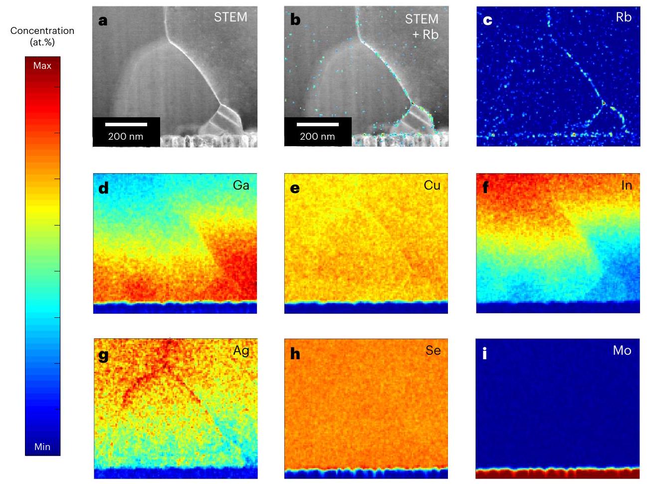
Microscopic characterization of the complete device stack
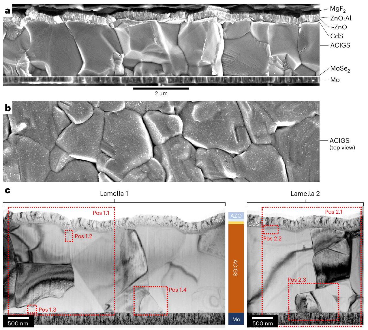
As shown in the scanning electron microscopy (SEM) images in Fig. 2a,b, large ACIGS grains are formed, with most of them being sized in all dimensions. The topography is not particularly smooth, but rather rough. The resulting tilted light in-coupling after refraction at the CdS/
Fig. 2 | Electron microscopy analysis of the device structure. a, b, SEM images of the full cross-section of the complete champion cell (a) and the absorber surface after selectively removing the CdS and window layers via HCl etching (b). The scale bar refers to both panels and . , BF-TEM images of the full cross-sections of the solar cell for the two lamellae investigated. The areas
for which the elemental distribution was analysed by scanning (S)TEM-EDS are highlighted with red boxes (‘Pos1.x’, lamella1; ‘Pos2.x’, lamella2). A schematic of the solar cell cross-section is illustrated between the two lamellae. The ZnO:Al film is abbreviated as AZO.
ACIGS interface is beneficial, since it increases the optical path length in the absorber.
To obtain a higher-resolved analysis of the absorber and interface structures, we prepared two thin ( ) cross-section lamellae of the full cell stack via a focused-ion beam (FIB). Figure. 2c shows the bright-field (BF) transmission electron microscopy (TEM) images of those two lamellae. The red dashed rectangles show the positions that were analysed by energy-dispersive X-ray spectroscopy (EDS), providing elemental distribution maps, which are illustrated either later in the manuscript or in Supplementary Information.
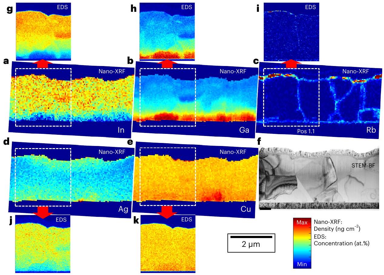
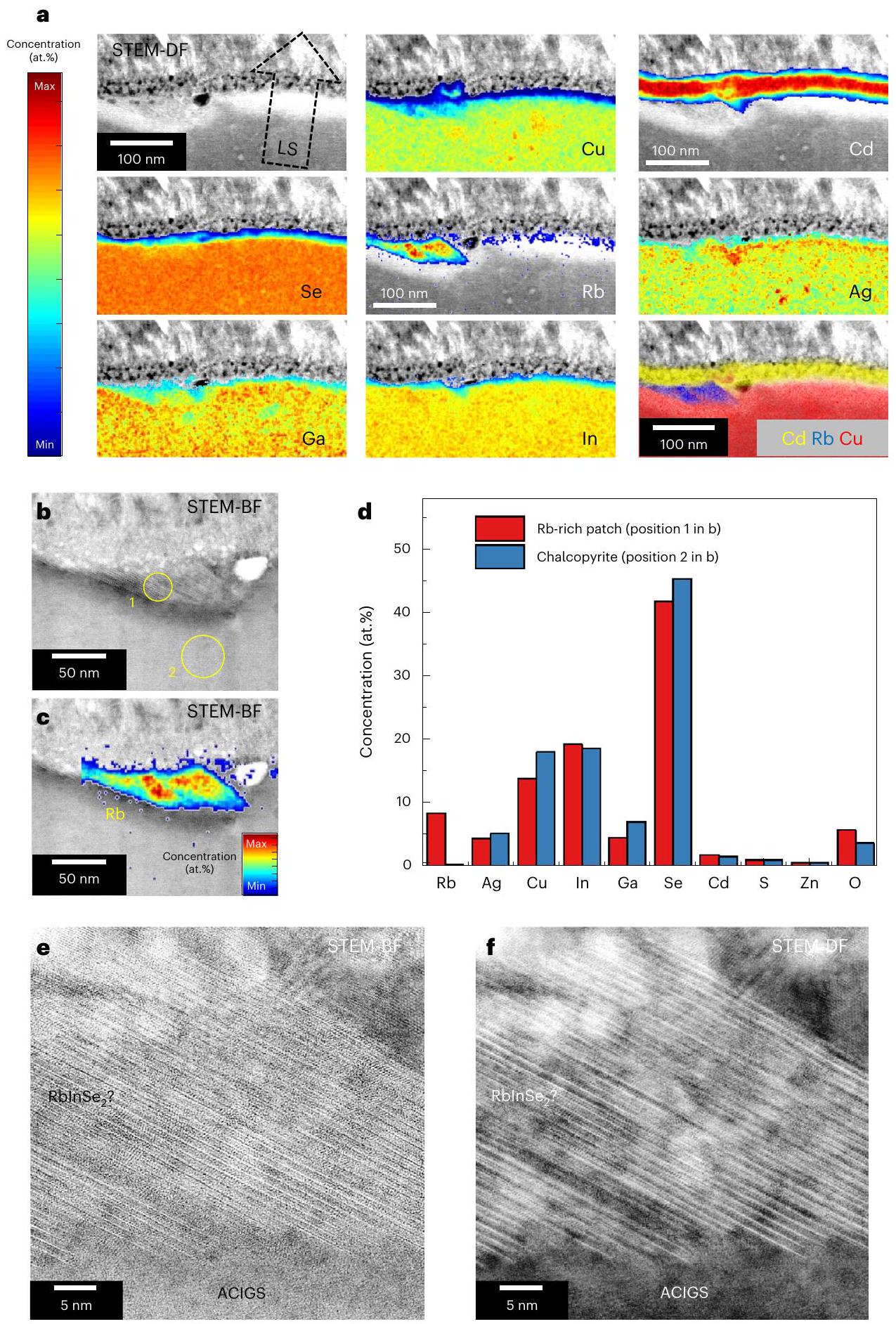
Lamella 1 was further studied on a nano-scale by X-ray fluorescence spectroscopy (nano-XRF). The measured relative elemental distributions of the absorber metal elements and Rubidium are displayed in Fig. 3. Semi-transparent Ga and Rb distribution maps, superimposed on the TEM image, can be found in Supplementary Fig. 4. In addition to the nano-XRF results, the elemental maps from ‘Pos1.1’, as obtained via EDS in scanning TEM (STEM) mode, are shown in Fig. 3 for comparison. A more detailed presentation of these STEM-EDS results at ‘Pos1.1’ can be found in Supplementary Fig. 5.
First, we observed that the nano-XRF and STEM-EDS experiments provide similar results regarding the absorber metal distribution. The exception is the Ag signal, which is too low in the case of the nano-XRF analysis to obtain reliable information, due to the superposition of the L edges of Ag, In and Cd. As intended, the upper half of the absorber exhibits a rather constant GGI level with only minor lateral variations, indicating only small fluctuations at the surface and in the .
Bandgap fluctuations may further arise from spatial variations in stress or stoichiometry . However, the observed minor compositional variations, together with the large ACIGS grain size, indicate moderate lattice stress (which may be larger in the direct vicinity of the CdS layer though). Moreover, the stoichiometry is found to be rather constant in the top half of the absorber ( )/ . A steep increase in GGI towards the Mo electrode is observed in the bottom third of the ACIGS, which should effectively repel electrons from the back contact. While suffering from a lower spatial resolution, an advantage of the nano-XRF method over STEM-EDS is the higher sensitivity to heavy alkali elements . It can be clearly seen that Rb agglomerates consistently (that is, no gaps) at the interfaces with CdS at the front and with at the back contact. Furthermore, it is found in certain grain boundaries (GBs), while others are Rb free. This feature was detected in previous studies where it was shown that heavy alkali atoms such as Rb and Cs do not diffuse into high-symmetry twin boundaries, but only decorate random high-angle .
The highest Rb concentration is found in isolated patches at the ACIGS/CdS heterojunction. Similar patches were reported in earlier studies for absorbers subjected to a CsF-PDT and suggested to indicate the formation of a phase . We provide a more detailed description of the Rb -containing patches later in the manuscript.
Even after 10 years of research, it is still under debate which effect(s) are responsible for the performance improvement by the heavy alkali PDT. Discussed mechanisms are a reduced GB band
Fig. 3 | Nano-XRF and STEM-EDS analysis of lamella 1. a-e, Elemental distribution of the absorber metals and , as obtained via nano-XRF on lamella1 from Fig. 2c. XRF peak fitting was conducted by using the dedicated software PyMca . To account for the small thickness variations across the lamella (XRF intensity/scales with sample volume), the signal intensity of the absorber metal elements was corrected at each pixel (that is, position) by multiplying it with an individual correction factor pixel pixel obtained from the Se distribution map. Here, is the highest intensity of the Se map and (pixel) is the intensity measured at each
corresponding pixel. This is a valid first approximation as long as the selenium concentration can be assumed to be constant everywhere in the absorber (that is, stoichiometry). Consequently, the Se distribution map is not shown. Corresponding STEM-BF image. , Corresponding maps of a smaller area (‘Pos1.1’, indicated by a dashed whit box) derived from STEM-EDS for In (g), Ga (h), and . The colour code refers to the atomic concentrations in at.% in case of the EDS analysis and to the density (in ) in case of the nano-XRF analysis, ranging from the corresponding minimum (Min) to the maximum (Max) values. The scale bar is valid for all images.
bending, lower Urbach energy, increased p-type doping and the formation of a wide-gap alkali-In-Se surface phase .
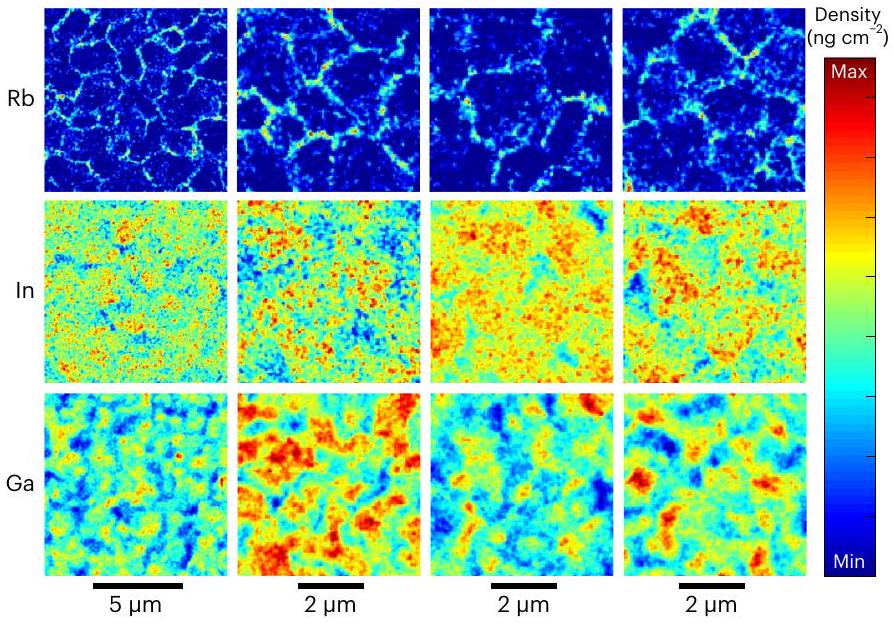
Figure 4 displays the elemental maps of Rb , In and Ga at four different absorber positions, as measured by nano-XRF of the bare absorber films (top view) after removing the window and buffer layers (compare Fig. 3b). We observe a clear anti-correlation between the Ga and In concentrations. This is not related to GGI fluctuations at the surface but illustrates the different depth at which the GGI suddenly increases towards the back contact (XRF signal stems from entire absorber volume). Rubidium seemingly agglomerates at GBs and its distribution is interrupted in places, indicating the presence of twin boundaries at the absorber surface. At some positions, the Rb signal is notably higher, suggesting the presence of the Rb-rich patches observed in the cross-section in Fig. 3. However, it cannot be excluded that those patches were selectively removed by the HCl etch, as proposed in earlier studies for alkali-In-Se surface phases . The weaker Rb signal from the grain interior most probably originates from the back interface as well as from tilted and deeper GBs.
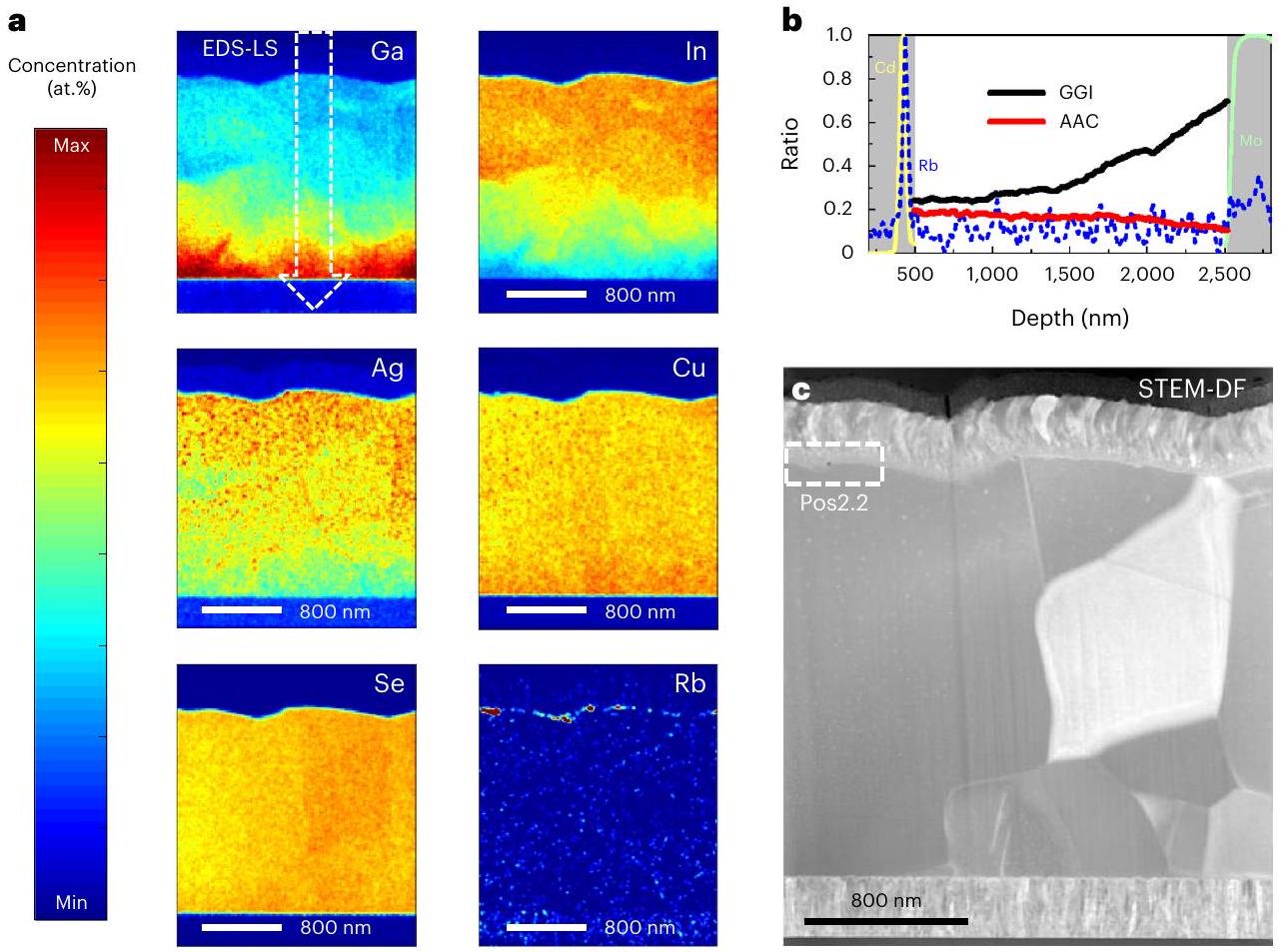
To investigate the Rb-rich patches in more detail and provide a quantification of the elemental depth-profiles, the positions ‘Pos2.1’ and ‘Pos2.2’ on lamella 2 were thoroughly analysed via STEM-EDS and the results are discussed in the following. The distribution of all absorber elements and Rb at ‘Pos2.1’ are shown in Fig. 5.
As seen for lamella, the upper half of the absorber shows a rather constant GGI and AAC (that is, also constant ). We extracted a line scan along the arrow drawn inside the Ga map. We did the same for ‘Pos1.1’ of lamella 1 (Supplementary Fig. 5) and quantified the average surface composition as from STEM-EDS. The region with only minor compositional fluctuations in the upper part
of the absorber is more extended in lamella1 (compare Supplementary Fig. 5). Generally, STEM-EDS analysis provides limited statistics about lateral differences in composition and microstructure, due to the small extracted sample volume and the time- and work-intensive nature of the technique. In the lower part of the ACIGS layer the GGI increases, while the AAC decreases. The reduced Ag content in regions of higher Ga concentration was observed in prior studies and can be explained by a thermodynamically driven, composition-dependent instability of the ACIGS system . The GGI at the back contact reaches a value close to 0.7 here, but deviates laterally (for example, GGI of 0.8 in Supplementary Fig. 5). Overall, the GGI at the MoSe/ACIGS interface ranges between 0.65 and 0.80 for all investigated locations.
To obtain a quantified average composition profile, glow-discharge optical emission spectroscopy was measured on the same sample. The results are illustrated together with the normalized intensities of Cd, Mo, Rb and Na (Na peaks at Mo/glass interface) in Supplementary Fig. 6. The obtained GGI and AAC profiles are very similar to the ones deduced from STEM-EDS. However, the surface GGI and AAC are slightly lower when extracted via GDOES, which may be an artefact of the destructive nature of the technique (for example, smearing out of interfaces). The bandgap value extracted from EQE can be used to calculate an estimation of the surface composition , since the Ga content is lowest at the buffer interface. For a value of GGI of is deduced, assuming AAC of 0.20 , which is closer to the surface composition derived from STEM-EDS.
As discussed previously, rubidium is mainly concentrated in patches ( in size) beneath the CdSlayer, but smaller amounts can be found everywhere at the ACIGS/CdSinterface (Fig.3).Bothprofiles (EDSinFig.5b and GDOES in Supplementary Fig. 6) show that the Rb signal peaks just
Fig. 4 | Lateral distribution of rubidium, indium and gallium. Elemental distribution of Rb, In and Ga (top view) at four different positions of the bare ACIGS absorber film (after removal of the window and buffer layers via an HCl etch), as obtained from nano-XRF analysis. Thickness differences were again corrected by using the intensity variations in the respective Se maps. The colour code refers to the density( in ), ranging from the corresponding minimum (Min) to the maximum (Max) values.
underneath the buffer layer, while GDOES also reveals an agglomeration at the back contact (that is, between and ACIGS), in line with the nano-XRF results. The Na concentration (Na added as a NaF precursor) in the absorber is below the GDOES detection limit, but it can be found in the Mo layer. At this stage, we do not understand why the Na content in the ACIGS bulk is exceptionally low, since typically the sensitivity provided by the GDOES method is sufficient to distinguish the Na signal from the measurement noise. Furthermore, it is not clear to what extent Na is present at the interface and in GBs, from where it was found to be pushed out by the heavier Rb in prior works . In earlier studies, a Na peak was found at the (A)CIGS surface in GDOES, due to the Na accumulation in ordered vacancy compounds (OVCs) . Rubidium was found to not (entirely) replace Na in these . This Na peak is absent in our measurement, and thus, we assume that the ACIGS film of our record device exhibits only a very minor amount of surface OVC patches, despite its relatively low [I]/[III] of 0.84.
Microscopic characterization of the heterojunction region
We analysed one of the Rb-rich patches found at the absorber surface in Fig. 5 in more detail (‘Pos2.2’) (Fig. 6). The elemental maps of the corresponding heterojunction region, obtained from STEM-EDS, are shown in Fig. 6a. It is evident that the Rb-rich area is depleted in Cu, in Ga and locally also in Ag. The quantified elemental concentrations inside and outside the Rb-rich patch (positions1 and2 in Fig. 6b) are shown in Fig. 6d. Relatively, the Cu and Ga contents are most reduced in the patch, where Rb reaches about . Considering that the lamella is thick, it is likely that the Rb -rich phase changes its lateral extension throughout the depth of the lamella. As a result, the volume analysed by EDS may contain a mixture of the ACIGS chalcopyrite phase and the Rb-rich patch, leading to an apparent concentration that is ‘artificially’ too low in Rb and too high in Cu and Ga . This is further highlighted by the inhomogeneous Rb concentration measured in the patch, as seen in Fig. 6c (highest local Rb concentration is 12 at.%). Thus, we speculate that the Rb -rich regions, frequently found at the CdS /absorber interface, are or another Rb-In-Se compound. However, we cannot exclude that this phase still contains some amount of and Ag . Figure 6e, f shows higher-magnified BF- and dark field (DF)-STEM images of the patch. An abrupt change in lattice structure from the chalcopyrite to
the Rb-In-Se phase is evident. A layered structure of atomic rows is identified inside the Rb-rich patch, as reported in earlier studies and attributed to the compound formation (monoclinic system, space group . It is unclear what kind of impact those patches have on the device performance. However, it is deemed unlikely that they have a beneficial effect, since they are rather widely dispersed and separated. In case the patches are indeed , a possible parasitic absorption would not be very detrimental though, due to its small extension and large bandgap of 2.8 eV (ref. 54).
We could not detect the Rb-rich phase via sheer phase contrast in (S)TEM alongside the CdS/absorber interface at positions outside those Rb -rich patches (see typical STEM images in Supplementary Fig. 7). Still, as we found via nano-XRF, rubidium seems to be present everywhere underneath the CdS.
To reveal chemical changes across the heterojunction, a STEM-EDS line scan was extracted along the black dashed arrow in Fig. 6a. The normalized elemental profiles are shown in Supplementary Fig. 8. The Rb agglomeration at the ACIGS/CdS interface is evident. Interestingly, the Cu and Ga signals drop about 5 nm before the other absorber elements. This is in line with the formation of a very thin (Ag,Rb)-In-Se compound (potentially ) at the absorber surface. We performed a similar analysis for ‘Pos1.2’ on lamella 1. The results are shown in Supplementary Figs. 9 and 10. Again, we found Rb agglomeration at the interface and the Cuand Ga signals drop before (here -3 nm ) the ones of In and Se. However, at this position the Ag also drops with the Cu and Ga signals. In all cases, the relative Ag signal is still quite high in the CdS film. This is probably caused by an artefact of the lamella preparation via the FIB, which triggers diffusion of mobile Ag atoms during thermal stress (or maybe even during e-beam exposure). Summarizing all findings, we speculate that a very thin ( ) phase forms everywhere alongside the CdS/ACIGS interface between the RbInSe patches.
Another feature observed in Supplementary Figs. 8 and 10 is the slight in-diffusion of Cd (depth ) into the thin layer (see differences in Cd and Ssignals). An interdiffusion of Cd and Cu has been observed before at CIGS/CdS interfaces . Earlier studies suggest that the resulting creation of donor defects in the chalcopyrite (or OVC) lattice leads to the formation of a beneficial buried homojunction and a strong type inversion at the absorber interface . However, these prior investigations did not consider or study the effect of Cd incorporation into the potential surface phase that probably has a completely different impact. Furthermore, we cannot exclude that Cd diffuses into the absorber only during the lamella preparation (similarly to a possible Ag smear-out).
Characterization of the back region and GBs
Finally, we address the chemical variations in the back-contact region and at ACIGS GBs. Figure 7 shows the elemental distributions in the vicinity of the Mo layer at ‘Pos1.4’ (lamella 1), as measured by STEM-EDS. Two more EDS mappings were conducted close to the Mo electrode at ‘Pos2.3’ and ‘Pos1.3’, which are shown in Supplementary Figs. 11 and 12, respectively. The results are very similar to the ones shown in Fig. 7.
First, we found abrupt strong changes in Ga and In (that is, in GGI) from one grain to another, as was reported in earlier studies for the bottom part of chalcopyrite absorbers . We detected again rubidium in most GBs, while it seems to be absent in one GB in Fig. 7 (in agreement with the corresponding nano-XRF in Fig. 3). Most of the investigated GBs are depleted in Cu , but enriched in Ag . Some GBs are further depleted in In and enriched in Ga , as can be clearly seen in Supplementary Fig. 11 and also for a GB close to the heterojunction in Supplementary Fig. 9. Overall, the Cu depletion is more or less balanced by the Ag enrichment, so that the [I]/[III] ratio does not change notably across the GBs (see, for example,[II/[III] map in Supplementary Fig. 9). Atom probe tomography (APT) characterizations of GBs in ACIGS absorbers with similar AAC of 0.2 (but KF-instead of RbF-PDT) reported in earlier studies showed clear reduction in Cu , increase in In (slightly in Se ) and no notable change in
Fig. 5 | STEM-EDS analysis of the complete solar cell. a, Distributions of the absorber elements and Rb at ‘Pos2.1’ (lamella 2), as deduced by STEM-EDS. The colour code refers to the atomic concentrations in at. , ranging from the corresponding minimum (Min) to the maximum (Max) values. b, GGI, AAC and normalized Cd , Mo and Rb depth profiles, extracted along the rectangle
indicated by the dashed white arrow in the Ga map in a (depth corresponds to direction of the arrow). The grey areas indicate the electrode/buffer regions. c, Corresponding STEM-DF image. The region ‘Pos2.2’, as indicated by the dashed white box, is shown in more detail in Fig. 6.
Ag and Ga (ref. 60). At this point, it is unclear why those prior studies led to partly different results. A possible reason why we found Ag -rich GBs in this study may be the diffusion of Ag into GBs during sample preparation. Yet, since APT sample preparation also requires FIB milling, the same effect would be expected in those prior APT studies. Moreover, STEM-EDS analysis of wide-gap ACIGS films reported in an earlier work showed Cu and Ag depletion in , which is in contrast to the findings shown in this work. A possible explanation is that only Ga-rich absorbers (that is, wide-gap) show Ag-depleted GBs and Ga-poor absorbers do not, similar to the anti-correlation seen in the grain interior . Indeed, we found the silver-enriched GBs in Fig. 7 (and Supplementary Fig. 11) only in regions of low Ga content, while GBs close to the back contact (high Ga concentration) do not show an Ag enrichment. More statistics are needed to draw further conclusions.
In prior publications it was proposed that Cu depletion at CIGSGBs often makes them benign (depends on oxygen and Na content) due to a favourable band bending . In addition, the Rb decoration of GBs was claimed to exclusively lead to beneficial upward band bending at . Other studies conclude that the of state-of-the-art chalcopyrite devices is still limited by GB recombination, despite a substantially reduced recombination velocity via an . More sophisticated methods are needed to study the effect of GBs on the overall recombination rate in the champion solar cell discussed in this work.
For the sake of a complete description of the absorber interfaces, STEM-BF images of the interface region are provided in Supplementary Fig. 13. A roughly 7-nm-thick MoSe layer (hexagonal structure with axis perpendicular to ) can be identified.
Strategies for chalcopyrite solar cells towards 25%
We presented the electro-optical, morphological and chemical properties of a -efficient ACIGS device. We believe that research and
innovation will lift efficiencies of chalcopyrite solar cells even higher in the future. As discussed in ‘Electro-optical characterization of the champion device’ section, the most straight-forward and possibly easiest way to improve the performance is to reduce the parasitic absorption in the buffer and window layer. Further strategies for manufacturing (A)CIGS-based solar cells towards (and beyond) efficiency are discussed in detail in Supplementary Note 1. This also includes a discussion of the effect of light soaking on the doping density and (illustrated in Supplementary Fig. 14).
Conclusions
We reveal the properties of a chalcopyrite-based solar cell with a certified efficiency of ( in-house measurement). The performance improvement is enabled by a high-concentration alloying of silver (AAC ) of the absorber film and the minimization of lateral and in-depth compositional fluctuations (that is, fluctuations) at the absorber surface and in the SCR. Instead of a conventional ‘notch’ GGI profile, we implement a ‘hockey stick’-like profile, with rather constant GGI in the upper half of the ACIGS film. We demonstrate that the RbF-PDT led to several absorber modifications. First, we show that the absorber surface is depleted in Cu and Ga (and locally Ag ) and enriched in Rb . The results suggest the presence of a phase (probably ) that is locally appearing in the form of larger patches (some ) and otherwise as a thin layer ( ). We also found rubidium in certain (presumably random high-angle) GBs and at the back-contact interface. Most of the analysed GBs are depleted in Cu but enriched in Ag, while some also show Gaenrichment and In depletion. Further studies are needed to assess the role of GBs and its chemistry on the performance of the solar cell.
Avoiding parasitic absorption in the window and buffer layers, while maintaining the same and FF level, seems to be the most
Fig. 6 | STEM-EDS analysis of the absorber/buffer heterojunction. a,
concentration has high transparency and vice versa). The black dashed arrow in the STEM-DF image indicates the position of an extracted EDS line scan, which is shown in detail in Supplementary Fig. 8.b, STEM-BF image of the Rb-rich patch identified in a. c, Same image with superimposed Rb concentration map from a. d, Quantified elemental concentrations, extracted from the circular regions 1 and 2 indicated in b. e,f, STEM-BF (e) and STEM-DF (f) images of the Rb-rich patch at higher magnification.
Distributions of absorber elements, Rb and Cd at ‘Pos2.2’ (lamella 2, see position also in Fig. 5c), as deduced by STEM-EDS. The maps are superimposed onto the corresponding STEM-DF image, and the colour code refers to the atomic concentrations in at. %, ranging from the corresponding minimum (Min) to the maximum (Max) values. In addition, a combination of the Cd, Rb and Cu signals is shown (transparency of different colors scales with concentration, that is low
Methods
Solar cell processing
The champion solar cell discussed in this work has the following stack sequence: soda lime glass/Mo/NaF-precursor/ACIGS/RbF-PDT/ . First, a 290 -nm-thick Mo back contact was
straight-forward approach to push the efficiency towards . To go beyond this level, the absorber quality has to be further improved and ERE values much higher than 1.6% (reported in the present study) need to be realized to further reduce the deficit and the ideality factor ( in the present work).
Fig. 7 |STEM-EDS analysis of the back-contact region. a, DF-STEM image of ‘Pos1.4’ (lamella 1). b, Semi-transparent rubidium concentration map, as deduced by STEM-EDS, superimposed on the STEM image. Pixels with Rb concentrations at the noise level are set fully transparent. The highest Rb concentration is found
at a triple junction. c-i, Distributions of elements close to the Mo back contact, as deduced by STEM-EDS. The color code of the elemental maps refers to the atomic concentrations in at.%, ranging from the corresponding minimum (Min) to the maximum (Max) values.
sputter-deposited (DC magnetron) and then coated with a 10 -nm-thick NaF precursor layer by thermal evaporation. No alkali diffusion barrier was introduced underneath the back contact. A modified three-stage (I-poor I-rich I-poor) co-evaporation process was applied to grow -thick ACIGS films at a maximum substrate temperature of about . All elements were provided in all three deposition phases. Further information about the sequence of the metal evaporation rates (ratios) can be obtained from an earlier work . The final absorber composition was GGI of 0.28 , AAC of 0.19 and [I]/[III] = 0.84 , as measured by XRF. After ACIGS deposition a heavy alkali PDT was applied by depositing of RbF at without breaking the vacuum and without additional Se supply. Subsequently, a ~25-nm-thick CdS buffer layer was grown via CBD at . Finally, a 30 – and 230 -nm-thick i-ZnO and ZnO :Al layer was RF- and DC-sputtered on top, respectively.
Afterwards, 27 individual cells with an area of were defined via a photolithography process and subsequent selective removal of the window layers by etching in acetic acid. On top of the transparent conductive oxide an aluminum grid with linewidth ( pitch) and in contact with a busbar frame outside the active/ aperture area of the cell was deposited via thermal evaporation. Finally, a 110 -nm-thick ARC was deposited across the whole area. The majority (22) of the 27 cells have efficiencies , very close to the cell discussed in this article that was certified by Fraunhofer ISE, and the correspondingJV parameters, as well as allJV curves, can be found in Supplementary Fig. 15 and Supplementary Table 1.
Electro-optical characterization of solar cells
All JV and EQE measurements were conducted after light soaking the complete cells for 24 h (no active cooling, that is cell temperature about ). In case of the in-houseJV measurement (red crosses in Fig. 1a), the entire solar cell, with an area of , was illuminated. For the certified measurement done by Fraunhofer ISE in Germany (black line
in Fig. 1a), a shadow mask with an aperture area of was used. The JV data of the in-house measurement were fitted using a one-diode model, by numerically solving the Shockley equation:
at each voltage value and globally minimizing the deviation of the results from the measured current densities . The in-house JV and EQE measurements were performed at using an ABET Technologies ‘Sun 3000 Solar Simulator’ (Xenon lamp) and a Bentham ‘PVE 300’ tool, respectively. For the EQE measurement the complete cell was illuminated with monochromatic light, so shading losses by the grid area are included in the corresponding spectrum (same for certified ISE measurement). The PL measurements were conducted in a setup consisting of a FSL1000 photoluminescence spectrophotometer from Edinburgh instruments equipped with an integrating sphere (coated with ) and a nitrogen cooled ( ) photomultiplier tube as a detector. The sample was excited by a 520 nm continuous wave laser at an intensity of about 1 sun (number of photons in laser beam matches the number of photons absorbed by the sample under illumination with the AM1.5G spectrum). The settings were chosen as 0.4 nm emission band width, 0.5 s dwell time and 1 nm step size. For the ERE measurement the emission band width was increased to 1 nm , the dwell time kept at 0.5 s and the step size was 1 nm for the emission range but 0.1 nm for the scatter range, to fully resolve the laser peak. First, the sample’s emission ( ) and reflection in the laser wavelength region ( ) was measured. Then, a plug was inserted instead of the sample to obtain the background in the emission range and the reference signal in the scattering range. In this way the absorption and emission (in number of photons) were obtained after integration, and the ERE was calculated by stands for the integrated yield in the emission range and Scat for the yield in the scattering range. Subscript A is for the sample and B is for the reference. To get the ERE value of , the integration was done between for the scattering range and for the emission range (see spectra in Supplementary Fig. 3).
Capacitance-voltage profiling was conducted from to +0.6 V at 60 kHz and an amplitude of 25 mV , using an Agilent 4284A precision LCR meter and a Keithley 2401 source meter. A dielectric constant of was assumed for the ACIGS material.
Material characterization
The integral ACIGS absorber composition was determined with a Helmut Fischer XRF, using a ‘Fischerscope X-ray 5400’ head. A Zeiss Merlin SEM (acceleration voltage of 5 kV ) was used to investigate the solar cell cross-sections and absorber surface after removal of the window and buffer layers via an HCl etch. STEM and EDS analyses were performed on a FEI Titan Themis XFEG instrument equipped with a Super-X detector and operated at 200 kV . The TEM lamellae were prepared via FIB in a Crossbeam 550 ZEISS system, following the lift-out technique. A final milling step at maximum 2 kV ion accelerating voltage was performed on both sides of the lamellae, and no further electron exposure was done in the FIB before the TEM analyses. The local composition of the ACIGS samples was further measured via nano-XRF at the NanoMAX beamline of the MAXIV synchrotron radiation facility in Lund (Sweden) . An X-ray energy of 16 keV with an average photon flux of photons and a spot size of was employed for the measurements and a piezo stage was used to move the sample with a 55 nm step size and a counting time of per pixel. The photon energy of 16 keV allowed to measure fluorescent photons corresponding to the K edges for and Se and L edges for Ag , In and Ga . The X-ray signal was recorded using a RaySpec single element SSD detector. The area densities (in ) of elements was estimated by fitting the XRF signal using the PyMca software . Laterally integrated elemental depth profiles (analysed area ) were deduced from a GDOES measurement in a Spectruma Analytik GDA 750HR system.
Reporting summary
Further information on research design is available in the Nature Portfolio Reporting Summary linked to this article.
Data availability
All data generated or analysed during this study are included in the published article and its Supplementary Information.Specific raw datasets are available from the corresponding author upon reasonable request.
References
Chirila, A. et al. Potassium-induced surface modification of thin films for high-efficiency solar cells. Nat. Mater. 12, 1107-1111 (2013).
Nakamura, M. et al. Cd-free Cu(In,Ga)(Se,S), thin-film solar cell with record efficiency of 23.35%. IEEE J. Photovolt. 9, 1863-1867 (2019).
Jackson, P. et al. Effects of heavy alkali elements in solar cells with efficiencies up to . Phys. Status Solidi RRL 586, 583-586 (2016).
Kato, T., Wu, J., Hirai, Y., Sugimoto, H. & Bermudez, V. Record efficiency for thin-film polycrystalline solar cells up to 22.9% achieved by Cs-treated Cu(In,Ga)(Se,S)2. IEEE J. Photovolt. 9, 325-330 (2019).
Hanket, G. M., Boyle, J. H. & Shafarman, W. N. Characterization and device performance of (AgCu)(InGa)Se absorber layers. In 34th IEEE Photovolt. Spec. Conf. 001240-001245 (IEEE, 2009).
Soltanmohammad, S., Tong, H. M., Anderson, T. J. & Shafarman, W. N. Reaction rate enhancement for absorber materials using Ag-alloying. IEEE J. Photovolt. 9, 898-905 (2019).
Chen, L., Lee, J. & Shafarman, W. N. The comparison of (Ag,Cu) (In,Ga)Se, and thin films deposited by three-stage coevaporation. IEEE J. Photovolt. 4, 447-451 (2014).
Kim, G. et al. Thin Ag precursor layer-assisted co-evaporation process for low-temperature growth of thin film. ACS Appl. Mater. Interfaces 11, 31923-31933 (2019).
Erslev, P. T., Lee, J., Hanket, G. M., Shafarman, W. N. & Cohen, J. D. The electronic structure of alloyed with silver. Thin Solid Films 519, 7296-7299 (2011).
Keller, J. et al. Wide-gap (Ag,Cu)(In,Ga)Se solar cells with different buffer materials-a path to a better heterojunction. Prog. Photovolt. Res. Appl. 28, 237-250 (2020).
Chen, S., Gong, X. G. & Wei, S. H. Band-structure anomalies of the chalcopyrite semiconductors versus and Se) and their alloys. Phys. Rev. B 75, 205209 (2007).
Huang, D. et al. General rules of the sub-band gaps in group-IV ( , and Sn )-doped -type chalcopyrite compounds for intermediate band solar cell: a first-principles study. Mater. Sci. Eng. B 236-237, 147-152 (2018).
Sugimoto, H., Tomita, H., Yamaguchi, K., Hirai, Y. & Kato, T. High-performance near-stoichiometric solar cells by sub-percent Ag-doping. In 29th PVSEC Conference 723-726 (PVSEC, 2019).
Green, M. A. Do built-in fields improve solar cell performance? Prog. Photovolt. Res. Appl. 17, 57-66 (2009).
Kobayashi, T. et al. Impacts of surface sulfurization on thin-film solar cells. Prog. Photovolt. Res. Appl. 23, 1367-1374 (2015).
Avancini, E. et al. Impact of compositional grading and overall Cu deficiency on the near-infrared response in solar cells. Prog. Photovolt. Res. Appl. 25, 233-241 (2017).
Reinhard, P. et al. Flexible solar cells with reduced absorber thickness. Prog. Photovolt. Res. Appl. 23, 281-289 (2015).
Gong, J. et al. Enhancing photocurrent of solar cells with actively controlled Ga grading in the absorber layer. Nano Energy 62, 205-211 (2019).
Friedlmeier, T. M. et al. Improved photocurrent in solar cells: from 20.8% to 21.7% efficiency with CdS buffer and Cd-free. IEEE J. Photovolt. 5, 1487-1491 (2015).
Chirilǎ, A. et al. Highly efficient solar cells grown on flexible polymer films. Nat. Mater. 10, 857-861 (2011).
Werner, J. H., Mattheis, J. & Rau, U. Efficiency limitations of polycrystalline thin film solar cells: case of . Thin Solid Films 480-481, 399-409 (2005).
Krause, M. et al. Microscopic origins of performance losses in highly efficient thin-film solar cells. Nat. Commun. 11, 4189 (2020).
Carron, R. et al. Heat-light soaking treatments for highperformance CIGS solar cells on flexible substrates. Preprint at Research Square https://doi.org/10.21203/rs.3.rs-2116168/v1 (2022).
Khatri, I., Shudo, K., Matsuura, J., Sugiyama, M. & Nakada, T. Impact of heat-light soaking on potassium fluoride treated CIGS solar cells with CdS buffer layer. Prog. Photovolt. Res. Appl. 26, 171-178 (2018).
Scheer, R. Activation energy of heterojunction diode currents in the limit of interface recombination. J. Appl. Phys. 105, 104505 (2009).
Nadenau, V., Rau, U., Jasenek, A. & Schock, H. W. Electronic properties of -based heterojunction solar cells. Part I. Transport. Anal. J. Appl. Phys. 87, 584-593 (2000).
Keller, J., Lindahl, J., Edoff, M., Stolt, L. & Törndahl, T. Potential gain in photocurrent generation for solar cells by using as a transparent conductive oxide layer. Prog. Photovolt. Res. Appl. 24, 102-107 (2016).
Keller, J., Stolt, L., Edoff, M. & Törndahl, T. Atomic layer deposition of transparent conductive oxide layers for application in solar cells with different buffer layers. Phys. Status Solidi A 213, 1541-152 (2016).
Chantana, J., Kawano, Y., Nishimura, T., Mavlonov, A. & Minemoto, T. Impact of Urbach energy on open-circuit voltage deficit of thin-film solar cells. Sol. Energy Mater. Sol. Cells 210, 110502 (2020).
Carron, R. et al. Advanced alkali treatments for high-efficiency solar cells on flexible substrates. Adv. Energy Mater. 9, 1900408 (2019).
Siebentritt, S. et al. Heavy alkali treatment of solar cells: surface versus bulk effects. Adv. Energy Mater. 10, 1903752 (2020).
Ugur, E. et al. Life on the Urbach edge. J. Phys. Chem. Lett. 13, 7702-7711 (2022).
Shockley, W. & Queisser, H. J. Detailed balance limit of efficiency of p-n junction solar cells. J. Appl. Phys. 32, 510-519 (1961).
Siebentritt, S. et al. How photoluminescence can predict the efficiency of solar cells. J. Phys. Mater. 4, 042010 (2021).
Siebentritt, S. et al. Photoluminescence assessment of materials for solar cell absorbers. Faraday Discuss. 239, 112-129 (2022).
Green, M. A. & Ho-Baillie, A. W. Y. Pushing to the limit: radiative efficiencies of recent mainstream and emerging solar cells. ACS Energy Lett. 4, 1639-1644 (2019).
Green, M. A. et al. Solar cell efficiency tables (Version 61). Prog. Photovolt. Res. Appl. 31, 3-16 (2023).
Schöppe, P. et al. Overall distribution of rubidium in highly efficient solar cells. ACS Appl. Mater. Interfaces 10, 40592-40598 (2018).
Schöppe, P. et al. Revealing the origin of the beneficial effect of cesium in highly efficient solar cells. Nano Energy 71, 104622 (2020).
Schöppe, P. et al. Rubidium segregation at random grain boundaries in absorbers. Nano Energy 42, 307-313 (2017).
Siebentritt, S. & Weiss, T. P. Chalcopyrite solar cells-state-of-the-art and options for improvement. Sci. China Phys. Mech. Astron. 66, 217301 (2023).
Reinhard, P. et al. Alkali-templated surface nanopatterning of chalcogenide thin films: a novel approach toward solar cells with enhanced efficiency. Nano Lett. 15, 3334-3340 (2015).
Keller, J. et al. Effect of KF absorber treatment on the functionality of different transparent conductive oxide layers in CIGSe solar cells. Prog. Photovolt. Res. Appl. 26, 13-23 (2018).
Larsson, F., Donzel-Gargand, O., Keller, J., Edoff, M. & Törndahl, T. Atomic layer deposition of buffer layers for solar cells with KF post-deposition treatment. Sol. Energy Mater. Sol. Cells 183, 8-15 (2018).
Sopiha, K. V. et al. Thermodynamic stability, phase separation and Ag grading in (Ag,Cu)(In,Ga)Se, solar absorbers. J. Mater. Chem. A 8, 8740-8751 (2020).
Pianezzi, F. et al. Unveiling the effects of post-deposition treatment with different alkaline elements on the electronic properties of CIGS thin film solar cells. Phys. Chem. Chem. Phys. 16, 8843-8851 (2014).
Raghuwanshi, M. et al. Influence of RbF post deposition treatment on heterojunction and grain boundaries in high efficient (21.1%) solar cells. Nano Energy 60, 103-110 (2019).
Vilalta-Clemente, A. et al. Rubidium distribution at atomic scale in high efficient thin-film solar cells. Appl. Phys. Lett. 112, 103105 (2018).
Keller, J., Aboulfadl, H., Stolt, L., Donzel-Gargand, O. & Edoff, M. Rubidium fluoride absorber treatment for wide-gap (Ag,Cu)(In,Ga) solar cells. Sol. RRL 6, 2200044 (2022).
Keller, J. et al. On the paramount role of absorber stoichiometry in (Ag,Cu)(In,Ga)Se, wide-gap solar cells. Sol. RRL 4, 2000508 (2020).
Taguchi, N., Tanaka, S. & Ishizuka, S. Direct insights into formation at thin film surface with RbF postdeposition treatment. Appl. Phys. Lett. 113, 113903 (2018).
Huang, F. Q., Deng, B., Ellis, D. E. & Ibers, J. A. Preparation, structures, and band gaps of and . J. Solid State Chem. 178, 2128-2132 (2005).
Weinberger, N. et al. Phase development in thin films-a temperature series. Scr. Mater. 202, 113999 (2021).
Kodalle, T. et al. Properties of co-evaporated thin films. Phys. Status Solidi RRL 13, 1800564 (2019).
Koprek, A. et al. Effect of Cd diffusion on the electrical properties of the thin-film solar cell. Sol. Energy Mater. Sol. Cells 224, 110989 (2021).
Nakada, T. & Kunioka, A. Direct evidence of Cd diffusion into thin films during chemical-bath deposition process of CdS films. Appl. Phys. Lett. 74, 2444-2446 (1999).
Migliorato, P., Shay, J. L., Kasper, H. M. & Wagner, S. Analysis of the electrical and luminescent properties of . J. Appl. Phys. 46, 1777-1782 (1975).
Ramanathan, K. et al. Advances in the CIS research at NREL. In 26th IEEE Photovolt. Spec. Conf. 319-322 (IEEE, 1997).
Keller, J. et al. Grain boundary investigations on sulfurized solar cells using atom probe tomography. Sol. Energy Mater. Sol. Cells 117, 592-598 (2013).
Aboulfadl, H. et al. Alkali dispersion in (Ag,Cu)(In,Ga)Se thin film solar cells-insight from theory and experiment. ACS Appl. Mater. Interfaces 13, 7188-7199 (2021).
Raghuwanshi, M., Wuerz, R. & Cojocaru-Mirédin, O. Interconnection between trait, structure, and composition of grain boundaries in thin-film solar cells. Adv. Funct. Mater. 30, 2001046 (2020).
Nicoara, N. et al. Direct evidence for grain boundary passivation in solar cells through alkali-fluoride post-deposition treatments. Nat. Commun. 10, 3980 (2019).
Abou-Ras, D. et al. Formation and characterisation of for based solar cells. Thin Solid Films 480-481, 433-438 (2005).
Edoff, M. et al. High in ( )( ) solar cells. IEEE J. Photovolt. 7, 1789-1794 (2017).
Johansson, U. et al. NanoMAX: the hard X-ray nanoprobe beamline at the MAX IV Laboratory. J. Synchrotron Radiat. 28, 1935-1947 (2021).
Solé, V. A., Papillon, E., Cotte, M., Walter, P. & Susini, J. A multiplatform code for the analysis of energy-dispersive X-ray fluorescence spectra. Spectrochim. Acta Part B 62, 63-68 (2007).
Acknowledgements
This work was financially supported by the Swedish Energy Agency contracts P2O20-90052 and P2021-90275 (SOLVE) (M.E.). We acknowledge MAX IV Laboratory for time on Beamline NanoMAX under Proposal 20220904 (N.M.M.). Research conducted at MAX IV, a Swedish national user facility, is supported by the Swedish Research council under contract 2018-07152, the Swedish Governmental Agency for Innovation Systems under contract 2018-04969, and Formas under contract 2019-02496. Support from S. Kalbfleisch at the beamline is highly acknowledged.
Author contributions
J.K. conducted the SEM, CV, GDOES and most of the JV and EQE characterization, sent samples to external certification, and analyzed, processed and visualized all data, and wrote the paper. K.K. did the PLQY and PL measurements and performed, together
with N.M.M. and M.B., the nano-XRF analysis. N.M.M. further assisted in data analysis of the nano-XRF results. O.D.-G. did all the TEM and corresponding EDS characterization, as well as the sample preparation via the FIB technique. O.L., E.W., L.S. and M.E. developed the ACIGS process, manufactured the complete solar cell sample and did some of the JV and EQE characterization, as well as the in-house XRF measurement. M.E. supervised the work. All authors reviewed the paper.
Funding
Open access funding provided by Uppsala University.
Competing interests
O.L. is a co-founder and CTO of Evolar AB. E.W. is a co-founder and head of R&D at Evolar AB. Evolar AB is a company commercializing thin-film solar cells. The other authors declare no competing interests.
Publisher’s note Springer Nature remains neutral with regard to jurisdictional claims in published maps and institutional affiliations.
Open Access This article is licensed under a Creative Commons Attribution 4.0 International License, which permits use, sharing, adaptation, distribution and reproduction in any medium or format, as long as you give appropriate credit to the original author(s) and the source, provide a link to the Creative Commons licence, and indicate if changes were made. The images or other third party material in this article are included in the article’s Creative Commons licence, unless indicated otherwise in a credit line to the material. If material is not included in the article’s Creative Commons licence and your intended use is not permitted by statutory regulation or exceeds the permitted use, you will need to obtain permission directly from the copyright holder. To view a copy of this licence, visit http://creativecommons. org/licenses/by/4.0/.
(c) The Author(s) 2024
natureportfolio
Corresponding author(s): Jan Keller
Solar Cells Reporting Summary
Nature Portfolio wishes to improve the reproducibility of the work that we publish. This form is intended for publication with all accepted papers reporting the characterization of photovoltaic devices and provides structure for consistency and transparency in reporting. Some list items might not apply to an individual manuscript, but all fields must be completed for clarity.
For further information on Nature Research policies, including our data availability policy, see Authors & Referees.
– Experimental design
Please check the following details are reported in the manuscript, and provide a brief description or explanation where applicable.
1. Dimensions
Area of the tested solar cells
No
Method used to determine the device area
X
No
2. Current-voltage characterization
Current density-voltage (J-V) plots in both forward and backward direction
Yes
No
Voltage scan conditions
Yes
No
Test environment
Yes
No
Protocol for preconditioning of the device before its characterization
Stability of the J-V characteristic
Yes
No
3. Hysteresis or any other unusual behaviour
Description of the unusual behaviour observed during
the characterization
Yes
No
Certified measurement (Fraunhofer ISE): (designated illumination area)
In-house measurement: A=1.03 cm2 (total area)
Explain why this information is not reported/not relevant.
Certified measurement (Fraunhofer ISE): Aperture area of the mask (opening)
In-house measurement: Determination of total cell area via camera.
Explain why this information is not reported/not relevant.
Negligible hysteresis
The measurement of the IV-curve is performed with a 4-quadrant power amplifier and a calibration resistor. The scan was performed in both directions. No difference was observed (no hysteresis). The final result is an average of both scan directions.
The performance of the solar cell does not depend on the voltage scan conditions as long as they are in a reasonable range.
From Fraunhofer ISE certificate: The calibration of the test sample was performed at Standard Testing Conditions (STC) under irradiation with a steady-state class AAA solar simulator. The temperature of the solar cell is determined by a sensor and is adjusted to . The irradiance is controlled with a monitor cell during the measurement in order to correct fluctuations linear. The divergence of the peripheral beams is . The solar cell is kept at a constant temperature on a vacuum chuck.
State-of-the-art ACIGS solar cells are stable in air. Thus, we did not emphasize on the detailled test environment, like humidity level and so on.
Prior to the measurement the solar cell was illuminated (light-soaked, solar simulator, i.e. white light) for 24 h without active cooling.
Explain why this information is not reported/not relevant.
As mentioned in the manuscript, the efficiency increases during the first 24 hours of light-soaking (after keeping the sample in the dark) and then saturates. No decrease in efficiency was observed after longer exposure to light (up to several days were tested).
The temporal stability of the solar cell performance was not controlled during the certification by Fraunhofer ISE.
Explain why this information is not reported/not relevant.
Hysteresis or other unusual behaviour not observed
Related experimental data
4. Efficiency
External quantum efficiency (EQE) or incident photons to current efficiency (IPCE)
A comparison between the integrated response under the standard reference spectrum and the response measure under the simulator
For tandem solar cells, the bias illumination and bias voltage used for each subcell
5. Calibration
Light source and reference cell or sensor used for the characterization
Confirmation that the reference cell was calibrated and certified
Calculation of spectral mismatch between the reference cell and the devices under test
6. Mask/aperture
Size of the mask/aperture used during testing
Yes No For the spectral mismatch correction the spectral distribution of the solar simulator is measured with a spectroradiometer, the spectral response of the DUT is measured with a monochromator.
Too much information for Methods section. We wanted to keep it concise.
Explain why this information is not reported/not relevant.
Yes
From Fraunhofer ISE certificate: The calibration of the test sample was performed at Standard Testing Conditions (STC) under irradiation with a steady-state class AAA solar simulator. The irradiance is controlled with a monitor cell during the measurement in order to correct fluctuations linear. The divergence of the peripheral beams is .
The solar cell is kept at a constant temperature on a vacuum chuck.
Too much information for Methods section. We wanted to keep it concise.
Fraunhofer ISE (Germany)
Too much information for Methods section. We wanted to keep it concise.
From Fraunhofer ISE certificate: The spectral mismatch – caused by the deviation of the class AAA simulator spectrum from the standard spectrum AM1.5G in combination with the difference between the spectral response of the reference cell and that of the device under test (DUT) – is calculated and corrected.
From the Fraunhofer ISE certificate: The absolute differential spectral responsivity is
Yes
No
Yes
No
Yes
No No
b) A time-modulated quasi-monochromatic measurement irradiation. The irradiance is determined by a primary calibrated reference solar cell (PTB).
The operating point of the solar cell is defined by a bias current under short circuit conditions.
Bias current : 0.3 mA , Nominal Value of the temperature of the object:
The voltage at the solar cell is set to below 0.03 VOC by a current-voltage-converter. The frequency of the chopped quasi-monochromtatic measurement light is at 133 Hz . The spectral bandwith (full width at half maximum) is below 5 nm . The temperature of the solar cell is determined by a sensor and adjusted to .
The description in the manuscript is shorter to keep the Methods section concise.
Certified Fraunhofer ISE:
Jsc,eqe from EQE (complete aperture area illuminated by monochromatic light)
Jsc,iv from IV
In-house:
Jsc,eqe from EQE (complete cell illuminated by monochromatic light) from IV
Explain why this information is not reported/not relevant.
Provide a description of the measurement conditions.
No tandem cell determined in a wavelength range from 300 nm to 1200 nm at a short circuit current bias. The measurement is done with laser-monoochromator setup with the DSR method in a two-beam geometry, using the two irradiation beams simultaneously:
a) A stationary bias irradiation with irradiances EB (not measured explicitly). The variation of EB allows different short circuit currents ISC (EB),
a) A stationary bias irradiation with irradiances EB (not measured explicitly). The variation of EB allows different short circuit currents ISC (EB),
b) A time-modulated quasi-monochromatic measurement irradiation. The irradiance is determined by a primary calibrated reference solar cell (PTB). conditions. Yes
No
Yes
No
vollow No No 1
The voltage at the solar cell is set to below 0.03 VOC by a current-voltage-converter. The frequency of the chopped quasi-monochromtatic measurement light is at 133 Hz
The spectral bandwith (full width at half maximum) is below 5 nm . The temperature of the solar cell is determined by a sensor and adjusted to .
The description in the manuscript is shorter to keep the Methods section concise.
Certified Fraunhofer ISE:
Jsc,eqe from EQE (complete aperture area illuminated by monochromatic light)
Jsc,iv from IV
In-house: from IV
Explain why this information is not reported/not relevant
Provide a description of the measurement conditions.
No tandem cell
Too much information for Methods section. We wanted (m)
Too much information for Methods section. We wanted to keep it concise.
From Fraunhofer ISE certificate: The spectral mismatch – caused by the deviation of combination with the difference between the spectral response of the reference cell
Provide a description of the related experimental data.
Hysteresis or other unusual behaviour not observed
Hysteresis or other unusual behaviour not observed
Hysteresis or other unusual behaviour not observed
(
herseris and that of the device under test (DUT) – is calculated and correction the spectral distribution of the simulator is
For the spectral mismatch correction the spect
Too much information for Methods section. We wanted to keep it concise.
Yes
No
Variation of the measured short-circuit current density with the mask/aperture area Yes
No
7. Performance certification
Identity of the independent certification laboratory that confirmed the photovoltaic performance
A copy of any certificate(s) Yes
No
8. Statistics
Number of solar cells tested Yes
No
Statistical analysis of the device performance Yes
No
9. Long-term stability analysis
Type of analysis, bias conditions and environmental conditions Yes
No
Report the difference in the short-circuit current density values measured with the mask and aperture area.
Only small variations observed
Fraunhofer ISE (Germany)
Explain why this information is not reported/not relevant.
Certificate copies should be provided in the Supplementary information. Please state the supplementary item number.
The certificates are available from the corresponding author upon reasonable request.
This manuscript focuses on a single ACIGS solar cell that obtained the record efficiency. As mentioned in the text, 26 more solar cells (most of them also with efficiency > 23%) were prepared from the same ACIGS deposition run.
Explain why this information is not reported/not relevant.
State where this information can be found in the text.
Since there is just a single cell discussed and presented, no statistical analysis was performed.
As mentioned in the manuscript, the efficiency increases during the first 24 hours of light-soaking (after keeping the sample in the dark) and then saturates. No decrease in efficiency was observed after longer exposure to light (up to several days were tested). Furthermore, the sample was stored for more than a year in a N2-cabinet and still reaches the same efficiency level (after light-soaking). No further stability tests (i.e. damp-heat, V-bias, etc) were done.
Explain why this information is not reported/not relevant.
Department of Material Science and Engineering, Division of Solar Cell Technology, Ångström laboratory, Uppsala University, Uppsala, Sweden. Evolar AB (now First Solar European Technology Center AB), Uppsala, Sweden. e-mail: jan.keller@angstrom.uu.se
Provide a description of hysteresis or any other unusual behaviour observed during the characterization.
Mask/aperture only used in certified measurements done at Fraunhofer ISE. Here, the size was A= 0.9 cm 2 .
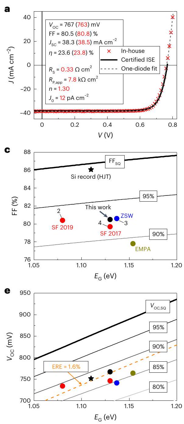
 (كل من