تعزيز الاستجابة والسرعة لمكتشفات الضوء غير المتجانسة WSe2/Ta2NiSe5 بمساعدة الفوتوجيتينغ في النفق Photogating-assisted tunneling boosts the responsivity and speed of heterogeneous WSe2/Ta2NiSe5 photodetectors

المجلة: Nature Communications، المجلد: 15، العدد: 1
DOI: https://doi.org/10.1038/s41467-023-44482-7
PMID: https://pubmed.ncbi.nlm.nih.gov/38167874
تاريخ النشر: 2024-01-02

يساعد التصوير الضوئي في تعزيز استجابة وسرعة الأنفاق غير المتجانسة كواشف ضوئية

تاريخ الاستلام: 25 يوليو 2023
تم القبول: 14 ديسمبر 2023
نُشر على الإنترنت: 02 يناير 2024

تحقق من التحديثات

مينغشيو ليو جينغشوان وي © ليوجيان تشي (ب) جونرو آن شينغسي ليو ياهوي لي Zhiminغ شي © دابينغ لي (ب) كوستيا س. نوفوسيلوف تشنغ-وي تشيو © وشاوجوان لي (ب)

الملخص

تأثير التصوير الضوئي هو الآلية السائدة في معظم كاشفات الضوء من المواد ثنائية الأبعاد (2D) ذات الاستجابة العالية. ومع ذلك، فإن الاستجابات الفائقة العالية في تلك الأجهزة تأتي بطبيعتها على حساب سرعة استجابة بطيئة جداً. في هذا العمل، نبلغ عن كاشف الهيكل غير المتجانس الذي يمكن تعزيز كسب الكشف الضوئي وسرعة الاستجابة في الوقت نفسه، متجاوزًا التبادل بين الاستجابة والسرعة. نكشف أن النفق المدعوم بالتحكم الضوئي يسمح بشكل متآزر بتكاثر حاملات الشحنة وتسريع الحاملات من خلال النفق تحت تأثير حقل كهربائي. يتميز تأثير التحكم الضوئي في جهازنا باستهلاك منخفض للطاقة (في حدود النانووات) ويظهر اعتمادًا على حالات الاستقطاب للضوء الساقط، والتي يمكن ضبطها بشكل أكبر من خلال جهود المصدر والمصرف، مما يسمح بتمييز الطول الموجي باستخدام هيكل مسطح ذو قطبين فقط. تقدم نتائجنا المزيد من الفرص لجيل جديد من الكواشف الضوئية التي طال انتظارها، مع استجابة عالية، وسرعة سريعة، واكتشاف الاستقطاب، واستشعار متعدد الألوان، في الوقت نفسه.

تشكل الكواشف الضوئية حجر الأساس لمجموعة متنوعة من الأجهزة البصرية والإلكترونية الضوئية، حيث يقود تطويرها الحديث بشكل رئيسي التقنيات الناشئة مثل الدوائر المتكاملة الضوئية. إنترنت الأشياء ، والأتمتة تستمر هذه التقنيات الجديدة في دفع الكواشف الضوئية لتحقيق استجابة أعلى، واستجابة أسرع، واستهلاك طاقة أقل، ووظائف إضافية مثل حساسية الطول الموجي والاستقطاب. ومع ذلك، لا يمكن تلبية المتطلبات المذكورة أعلاه في نفس الوقت في الكواشف الضوئية التقليدية المعتمدة على المواد الضخمة، مثل السيليكون. جرمانيوم وأشباه الموصلات من النوع III-V يمكن أن تكون الحلول الواعدة هي استخدام المواد ثنائية الأبعاد (2D) التي تتمتع بتفاعلات قوية بين الضوء والمادة، وفجوات نطاق قابلة للتعديل، وتوافق مع إنتاج أشباه الموصلات الحالي.
الخطوط، والفرص الغنية التي توفرها الواجهات غير المتجانسة الحادة ذريًا . على سبيل المثال، كواشف الضوء من المواد ثنائية الأبعاد ذات الاستجابة الفائقة العالية ( لقد تم توثيقها بشكل جيد، حيث يهيمن تأثير فتحات الضوء على الاستجابة الضوئية تنتج نتائج أداء الاستجابة الممتازة من الزيادة الكبيرة في اكتشاف الضوء: ، حيث و مدة حياة حاملات الشحنة ووقت عبور الحاملات، على التوالي لسوء الحظ، يتم تحقيق مثل هذه الآلية دائمًا مع عمر طويل لحاملات الشحنة الضوئية، مما يؤدي إلى معاناة من وقت استجابة مطول. ، مع قيم نموذجية في نطاق المللي ثانية، غير مبررة للعديد من التطبيقات مثل التصوير. يتم توضيح التوازن بين الاستجابة العالية والسرعة السريعة في الشكل 1a. يتم فحص مكاسب الكشف الضوئي عن كثب
الشكل 1 | سلوك النقل القابل للتعديل في هيكلنا ثنائي الأبعاد
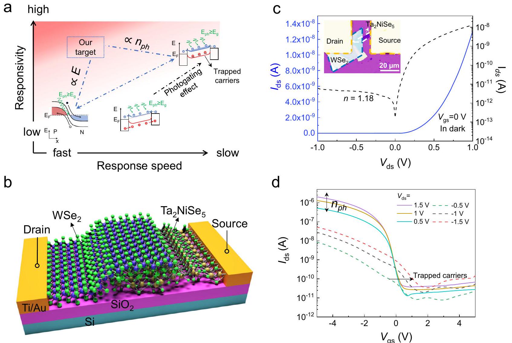
كاشف. توضيح للتوازن بين الاستجابة والسرعة في كواشف الضوء من المواد ثنائية الأبعاد. للتغلب على هذا التوازن والدخول إلى المنطقة العليا اليسرى، نحتاج تقليديًا إلى زيادة استهلاك الطاقة، المشار إليه باللون الأحمر. مخطط نطاق الطاقة في الجانب السفلي الأيسر هو وضع الخلايا الشمسية لكاشف الضوء، والوسط هو وضع التوصيل الضوئي، والجانب العلوي الأيمن ينتمي إلى وضع التحكم الضوئي. هو طاقة الفوتون، هو تركيز الحاملات الناتجة عن الضوء، هو فجوة الطاقة، هو مستوى فيرمي للمادة، و هو المجال الكهربائي الخارجي. تمثل الألوان الخلفية المختلفة اتجاه التغير في استهلاك الطاقة المحتمل المطلوب للكواشف الضوئية ثنائية الأبعاد، والذي يزداد تدريجياً من اللون الأبيض في الزاوية السفلى اليمنى إلى اللون الأحمر في الزاوية العليا اليسرى من الشكل. مخطط لـ
تظهر المعادلة أن الاستجابة يمكن أيضًا زيادتها من خلال تقليل زمن الانتقال. تقليديًا، يتم تحقيق ذلك باستخدام أجهزة ذات أطوال قنوات أقصر أو فولتية انحياز أكبر، والتي تواجه قيودًا في التطبيقات العملية. لا يمكن تقليص طول القناة بشكل تعسفي بسبب قدرة التصنيع، وزيادة التيارات المظلمة وبالتالي استهلاك الطاقة. ; عادة ما يبقى جهد الانحياز عند في دوائر أشباه الموصلات المعدنية-أكسيد-المعادن (CMOS) حوالي . علاوة على ذلك، بينما تلعب الاستقطاب وطول موجة الضوء أدوارًا أساسية في التطبيقات الواسعة، فإن معظم الكواشف الضوئية الحالية حساسة فقط لشدة الضوء لذلك، كيفية التغلب على توازن الاستجابة والسرعة وتوسيع وظائف الكواشف الضوئية لا يزال مشكلة بارزة.
في هذا العمل، نبلغ عن WSe ثنائي الأبعاد جهاز الهيكل غير المتجانس الذي يمكن أن يلبي جميع المتطلبات المذكورة أعلاه. تشير تحليلاتنا إلى أن عملية النفق يمكن أن تقلل بشكل كبير من زمن الانتقال في جهازنا، مما يعزز بشكل كبير من كسب اكتشاف الضوء وبالتالي الاستجابة. ونتيجة لذلك، لدينا ميزانية استجابة كافية لتقليل زمن الاستجابة إلى ما دون العتبة التي تبلغ حوالي 1 مللي ثانية للتطبيقات التصويرية العملية من خلال إدارة مواقع الفخ. أي، بسبب
بفضل زمن الانتقال القصير الممكن بفضل النفق، يتيح جهازنا استجابة عالية حتى في ظل عمر حامل قصير نسبيًا. تصل الاستجابة إلى أكثر من ، ووقت الاستجابة انخفض إلى بينما الأداء المذكور أعلاه يتفوق بالفعل على أجهزة التصوير الضوئي ثنائية الأبعاد الحالية في حالة تطبيقات التصوير، فإن جهازنا يظهر أيضًا استهلاكًا أقل للطاقة في حدود النانو واط، ونطاق عمل واسع من الضوء المرئي إلى الأشعة تحت الحمراء، واعتماد على الاستقطاب بسبب التباين الداخلي. . من المثير للاهتمام أن نسبة الاستجابة الضوئية غير المتساوية قابلة للتعديل حسب الجهد وتعتمد على الطول الموجي، مما يوفر منصة واعدة لتمييز الأطوال الموجية. قد تمهد نتائجنا الطريق نحو تطوير مستشعرات ضوئية ثنائية الأبعاد عالية الأداء في المستقبل، والتي يمكن أن تكون لها تطبيقات في الطيفية المصغرة، والتصوير الطيفي، وتحديد الأجسام والتهديدات.

النتائج

سلوك النقل القابل للتعديل حسب التحيز جهاز

الشكل 1 ب يوضح المخطط لـ الكاشفات الضوئية ذات الهيكل غير المتجانس. الطبقات و تم تقشير الرقائق ميكانيكياً من موادها الأساسية، وكانت الأقطاب الكهربائية مكونة من التيتانيوم/الذهب. . كعضو في
الكالكوجينيدات الثلاثية، يمتلك هياكل أحادية الميل متعددة الطبقات تحت درجة حرارة الانتقال ، حيث تتشكل الطبقات بواسطة التجميع الدوري سلاسل الديمر السلاسل الفردية مرتبطة بشكل ضعيف عبر تفاعلات فان دير فالز (الشكل التكميلي 1a). الهيكل المشوه للسلسلة يؤدي إلى وجود أنيسوتروبية قوية في المستوى وجميع ثوابت الشبكة الثلاثة ( ÅÅ، و Å ) مختلفة يمكن تحديد الاتجاه البلوري بواسطة المجهر الضوئي وطيف رامان المستقطب ذو الزاوية في تجاربنا، حيث يتوافق المحور الطويل للرقاقة المتقشرة مع الاتجاه (ملاحظة إضافية 1) . بالإضافة إلى ذلك، تحافظ على فجوة النطاق المباشرة من 0.36 إلكترون فولت في الكتلة إلى طبقة أحادية مع reported high carrier mobility رسم هيكل الذرة لـ يمتلك تناظر سداسي متساوي الأبعاد في المستوى Å ) مع طبقتين لكل وحدة مكررة (الشكل التكميلي 1b). طبقات قليلة لديه فجوة نطاق كبيرة من معامل امتصاص عالي وثبات جيد في الظروف المحيطة نقل الشحن الفعال في تم تأكيد واجهة وجودة المواد العالية من خلال القياسات البصرية (الملاحظة التكميلية 2) .
تمت دراسة أجهزة الهياكل المتعددة التي تتكون من سماكات مختلفة (الملاحظة التكميلية 3). يوضح الشكل 1c تيار المصدر-المصرف ( ) لجهاز تمثيلي في الظلام عند درجة حرارة الغرفة (انظر الصورة المصغرة في الشكل 1c لصورة بصرية من الأعلى). تظهر الأجهزة خصائص تقويم نموذجية مع عامل مثالية من . ثم قمنا بقياس الخصائص البصرية الكهربائية للجهاز تحت إضاءة مصدر ضوء أبيض. خصائص النقل ( ) للجهاز موضحة في الشكل 1d. المنحنيات الناتجة المقابلة ( ) موضحة في الشكل التوضيحي 6. من توقيعات المنحنى، وجدنا الظواهر التالية: أولاً، الهياكل غير المتجانسة تظهر بوضوح خصائص النقل من نوع – ونسبة تشغيل/إيقاف عالية الذي يُنسب إلى القدرة العالية على ضبط البوابة -نوع القطبية الكهربائية لـ و تم التحقيق فيها بشكل منفصل (الملاحظة التكميلية 4). تؤكد النتائج الضعيف خاصية النقل من نوع “ بارز موصلية من نوع وهو ما يتماشى مع التقارير السابقة تم تقدير حركة الناقل على أنها و لـ و WSe “، على التوالي. ثانيًا، تشير الخصائص إلى نقل يهيمن عليه حاجز شوتكي عند الانحياز الإيجابي ( ) شرط تيار خرج عالي تحت الجهد الموجب الجهد عند جهة الاتصال المعدنية يؤكد تشكيل نوع الاتصال الذي يكون ملائمًا لحقن الثقوب في الاتصال المعدني، الذي سيتم مناقشته بمزيد من التفصيل في الأقسام التالية. ثالثًا، يظهر الجهاز سلوكيات مميزة تحت فولتية انحياز المصدر-المصرف المختلفة (الشكل 1d). تحت السلبية يمكن اعتبار التصوير الضوئي كتحول أفقي في آثار تحت الإضاءة مع زيادة شدة . تشير هذه الظاهرة إلى وجود حالات فخ يمكن أن تقيم فيها الحوامل لفترات طويلة عند العيوب أو عند واجهة الهيكل غير المتجانس . ومع ذلك، تحت الإيجابي تحول أفقي في تم قمع الآثار إلى حد كبير، وزيادة عدد حاملات الضوء ( ) تحت ضغط إيجابي أعلى يؤدي إلى تيار خرج أكبر. تظهر الملاحظات أعلاه سلوك النقل القابل للتعديل بواسطة الانحياز لـ البنية غير المتجانسة.

التنقل المدعوم بالتصوير في جهاز

لتوضيح سلوك الجهاز القابل للتعديل حسب الانحياز بشكل أكبر، نقوم برسم خريطة التيار الضوئي والمخططات البيانية المقابلة لجهاز نموذجي في الشكل 2. يتكون الجهاز من وصفتين معدنيتين/ شبه موصلتين على جانب المصدر/ المصرف وواحدة بسمك 60 نانومتر. -سمك نانومتر التوصيل غير المتجانس. رسم خرائط التيار الضوئي المحلّل مكانيًا مع إضاءة ليزر بزاوية 532 نانومتر ( ) في أماكن مختلفة تكشف عن صور توليد تيار ضوئي مختلفة بشكل ملحوظ (الشكل 2 أ، ب). تم الحصول على نتائج مماثلة تحت إضاءة ليزر 633 نانومتر (الملاحظة التكميلية 5). كان توليد التيار الضوئي الملحوظ في المنطقة المتداخلة يتم ملاحظة المنطقة عند
. على العكس من ذلك، عندما يكون الجهاز في حالة انحياز أمامي، يتم توليد الحد الأقصى من التيار الضوئي بالقرب من منطقة الوصلة حيث يتصل القطب المعدني بـ WSe (الشكل 2ب). تشير هذه الملاحظات إلى آليات التشغيل القابلة للتعديل في الهياكل غير المتجانسة، مما يدل على سلوك النقل المتميز في الشكل 1d أعلاه.
محاذاة النطاقات لطبقات قليلة تمت دراسة الهياكل غير المتجانسة باستخدام طرق نظرية الكثافة الوظيفية (DFT). تم تعديل دالة بيردو-بورك-إرنزرهوف (PBE) لوصف تفاعل تبادل-ترابط الإلكترونات نظرًا لموثوقيتها الكبيرة مع ثنائي كبريتيدات المعادن الانتقالية (TMDCs) بما في ذلك إنSe وما إلى ذلك الهياكل النطاقية المتوقعة لـ 1-6 طبقات تظهر الهياكل غير المتجانسة في الملاحظة التكميلية 6. الحد الأدنى من نطاق التوصيل (CBM) والحد الأقصى من نطاق التكافؤ (VBM) لـ تضمين في فجوة الطاقة لـ على الرغم من السماكة، مما يدل على المحاذاة من النوع الأول. بالنسبة للهياكل غير المتجانسة الأكثر سمكًا الموضحة في الشكل 2a و b، فإن المواقع النسبية لحد أدنى نطاق التوصيل (CBM) وحد أقصى نطاق التكافؤ (VBM) لـ WSe السميك (بسمك 60 نانومتر) هي و 5.2 إلكترون فولت، على التوالي، مع فجوة طاقة مقدارها . وفقًا لدراسات تجريبية حديثة حول نطاق الطاقة لـ ، CBM و VBM للسمك الأكثر سميك) هم و 4.93 إلكترون فولت مع فجوة طاقة قدرها 0.33 إلكترون فولت. الفرق في مستويات فيرمي بين الـ و يتم قياسه ليكون (الملاحظة التكميلية 5). يتم تحديد مخطط النطاق للجهاز كما هو موضح في الملاحظة التكميلية 5، والتي تظهر أيضًا تشكيل تقاطع غير متجانس من النوع الأول.
وبناءً عليه، يتم تصوير مخطط نطاق الطاقة عندما يكون الجهاز متحيزًا سلبًا في الشكل 2c. نظرًا لأن اتجاه التحيز الخارجي مطابق للمجال الكهربائي المدمج في التوصيل غير المتجانس، يؤدي تعزيز المجال الكهربائي إلى فصل فعال لزوجي الإلكترون والثقب الناتجين عن الضوء عندما يتم تسليط الضوء الساقط على منطقة التوصيل غير المتجانس. على العكس، عندما يكون الجهاز في حالة انحياز أمامي. نظرًا للمجال الكهربائي المدمج لـ الوصلة غير المتجانسة تكون عكس المجال الكهربائي الخارجي المطبق عبر الجهاز، الإلكترونات المثارة ضوئيًا في تنجرف نحو واجهة وتجمعت عند واجهة التداخل بسبب الحاجز الكبير للإلكترونات (الشكل 2d). في هذه الحالة، تعمل الإلكترونات المحصورة عند الواجهة كبوابة سلبية، مما يؤدي إلى تأثير بوابة ضوئية. كاستجابة لهذا السلوك، مستوى فيرمي لـ سوف ينخفض، مما يزيد من تركيز الثقوب، مما يعزز نفق حاملات الثقوب من القطب السالب إلى والتي يتم نقلها بعد ذلك إلى القطب المصدر. من الجدير بالذكر أن نفق الحاملات قد ثبت أنه قابل للتطبيق في تحسين سرعة استجابة الجهاز في التقارير الأخيرة. للتحقق من نفق الحامل في جهازنا، تم قياس منحنيات الاستجابة الضوئية تحت إضاءة ضوئية بأطوال موجية مختلفة (الشكل 2e، f والشكل التكميلي 10). المنحنيات عند فولتية انحياز إيجابية تم نمذجتها بشكل جيد بواسطة حاجز نفق باستخدام تقريب سيمونز (الشكل 2g). رسم التوافق لـ ضد يظهر اعتمادًا خطيًا مع ميل سلبي تحت ظروف أكبر وترتفع بشكل أسي تحت تأثير صغير تحت الإضاءة الخفيفة، كما هو موضح في الأشكال. وبالتالي، يحدث النفق السائد مع النفق المباشر (DT) عند جهد منخفض و نفق فاولر-نوردهايم (FNT) عند جهد أعلى (انظر التحليل التفصيلي في الملاحظة التكميلية 7) “. تشير الملاحظات أعلاه إلى أن نقل الشحنات المسيطر عليه من خلال النفق عند واجهة المعدن/ يسيطر على سلوك الجهاز تحت التحيزات الإيجابية.
لاستكشاف تأثير الضوء الساقط على حاجز النفق للجهاز بشكل أعمق، قمنا بحساب تغيير تركيز الحاملات في المادة تحت كثافات ضوء ساقط مختلفة. يمكن تقدير التغيير في تركيز الحاملات بواسطة ، حيث هو الشحنة الكهربائية ) ، هو سعة البوابة ( لـ ” هو جهد العتبة، الذي يمكن استخراجه من منحنى النقل لجهاز الوصلة غير المتجانسة في الشكل 2f والشكل التكميلي 10. التغير في تركيز الثقوب ( يتم التعبير عنه كـ ، حيث يمثل المادة
الشكل 2 | التوصيل عبر النفق المدعوم بالتصوير الهياكل غير المتجانسة. صور رسم خرائط التيار الضوئي المحللة مكانيًا عند (أ) و (ب) شريط المقياس هو . طول موج الإضاءة هو 532 نانومتر. الخطوط المتقطعة البيضاء والزرقاء والصفراء تشير إلى المناطق من وأقطاب معدنية، على التوالي. مخططات نطاق الطاقة لـ جهاز الهيكل غير المتجانس عند (ج) و (د) ، على التوالي. تشير السهم إلى اتجاه نقل الحاملات، ويمثل الخط الأفقي المتقطع مستوى فيرمي للمادة. e منحنيات الخرج ( في الظلام وتحت الإضاءة مع كثافات طاقة مختلفة. الضوء الساقط عند 532 نانومتر
طول الموجة، و منحنيات النقل ) للجهاز في وتمثل المنطقة المظللة نطاق تغيير نقطة حيادية الشحنة. مخططات فاولر-نوردهايم للجهاز عند الإيجابية في الظلام وتحت الإضاءة. الخطوط المتقطعة هي التوافقات مع البيانات التجريبية. التغيرات في كثافة الثقوب ( ) في الجهاز كزيادة في قوة الضوء الساقط عند أطوال موجية مختلفة. الخطوط الصلبة مرسومة لتوجيه العين. عمر حاملات الضوء المستخرجة (الخطوط الصلبة) ووقت عبور الحاملات (الخطوط المتقطعة) للجهاز تحت ظروف مختلفة تم رسم الخطوط الصلبة والمقطعة لتوجيه العين.
سمك، والذي يبلغ 60 نانومتر لـ في الجهاز الذي تم التحقيق فيه. من الواضح من الشكل التوضيحي 10 أنه مع زيادة شدة الضوء الساقط، يتحرك تدريجياً نحو جهد البوابة الإيجابي. وفقًا للتغير في قمنا بحساب تغيير تركيز الحاملات لطاقات ضوء مختلفة، كما هو موضح في الشكل 2h. بناءً على ذلك، يمكننا أن نستنتج أن يزداد مع تعزيز كثافة الطاقة الضوئية. عرض حاجز النفق، يتم تقليله وفقًا لذلك، بناءً على العلاقة بين وبالتالي، فإن عرض الحاجز الأرق أو احتمال النفق الأعلى يساعدان بشكل أكبر في نفق الحاملات، مما يؤدي إلى نفق مدعوم بالتصوير الضوئي في الجهاز.
استنادًا إلى ما سبق، فإن الزيادة المتزامنة في استجابة الجهاز وسرعة الاستجابة تحت ظروف إيجابية من المتوقع حدوث ذلك بسبب تأثير النفق المدعوم بالتصوير الضوئي. من ناحية، تتناسب الاستجابة مع الكسب، الذي تم تعزيزه بشكل كبير في جهازنا بسبب تقليل زمن العبور عبر عملية النفق؛ من ناحية أخرى، يتم أيضًا تقليل عمر الحامل من خلال إدارة مواقع الفخاخ التي تساعد في إعادة تركيب الحوامل المثارة بالفوتون، مما يؤدي إلى سرعة استجابة سريعة. بعبارة أخرى، يتم حجب عدد كبير من الإلكترونات المولدة بالضوء في نطاق التوصيل بواسطة حاجز نطاق الطاقة تحت انحياز إيجابي، والذي يعمل كدور مواقع الفخاخ الضحلة التي تلتقط الحوامل الناتجة عن الضوء لفترة أقصر
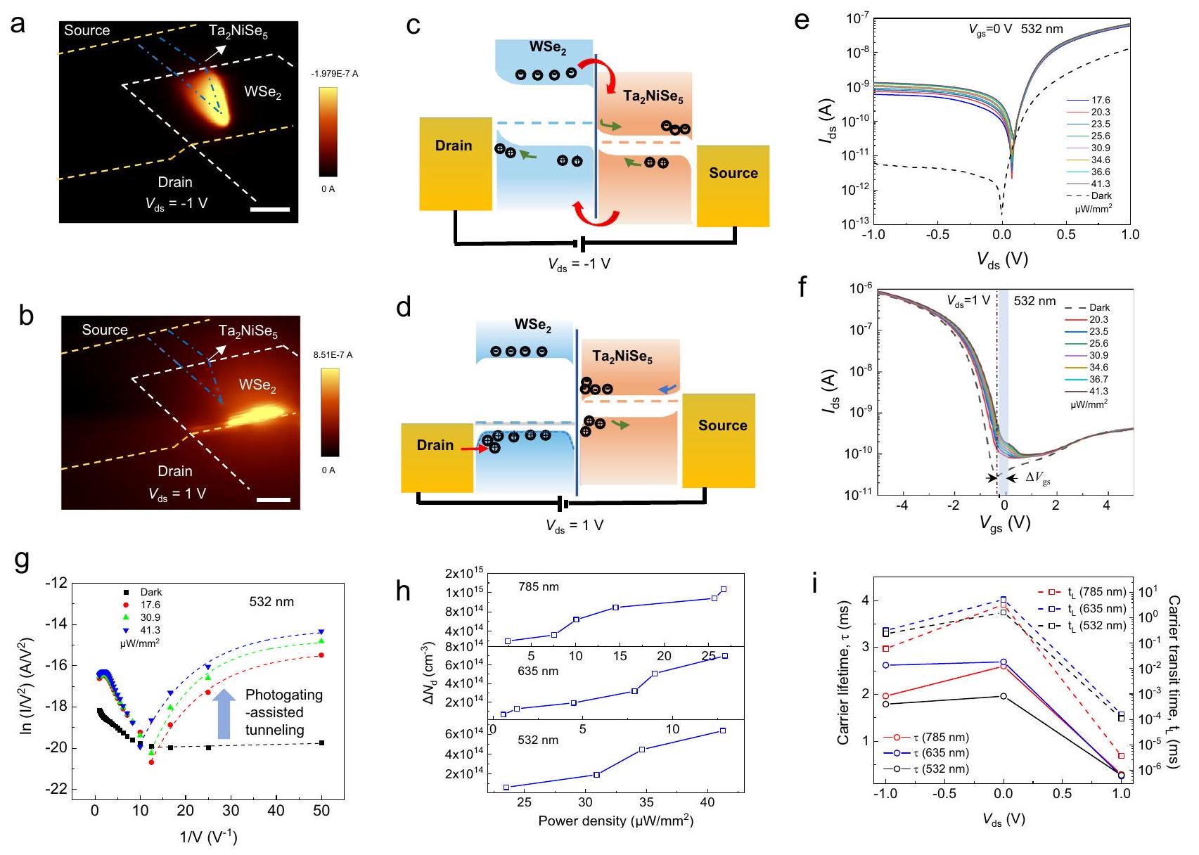
عمره. بالمقارنة، تلعب الفخاخ الداخلية للحاملين ذات مستويات الطاقة الضحلة والعميقة في المواد دورًا رئيسيًا تحت الجهد السالب، مما يتميز بعمر أطول نسبيًا. تقيس أوقات انتقال الحاملين وعمر الحاملين الضوئيين للجهاز تحت ظروف مختلفة. كما هو موضح في الشكل 2i، يتوافق بشكل جيد مع التحليل أعلاه (تفاصيل عملية الاستخراج موضحة في الملاحظة التكميلية 8).

علاقات سرعة الاستجابة جهاز

للنظر في علاقات الاستجابة والسرعة، نقوم بمزيد من تحليل الخصائص البصرية الكهربائية لـ أجهزة الهيكل غير المتجانس تحت إضاءة ضوء أحادي اللون (انظر التفاصيل في الملاحظة التكميلية 9). وفقًا للاستجابة الضوئية المعتمدة على القدرة، فإن الاستجابات، ، ضد كثافة الطاقة يتم الحصول عليها في أوقات مختلفة (الشكل 3أ). من الجدير بالذكر أنه يتم الحصول على استجابة عالية مع ( ) عندما يتم تطبيقه، وهو بأعداد مرتبة أعلى بكثير من ذلك في تحسين مماثل عند الإيجابية يلاحظ أيضًا في عدة أجهزة (الشكل 3ج). تقل القيم مع تعزيز قوة الضوء عند ، وعُزِيَت هذه الظاهرة عمومًا إلى تقصير عمر الحاملات الناتجة عن الضوء بسبب عمليات أوغر أو بسبب تشبع حالات الفخ تحت تدفق فوتوني عالٍ كثافات الطيف الضوضائي للجهاز هو
ب
د
ف
الشكل 3 | علاقات الاستجابة والسرعة لـ الهياكل غير المتجانسة. استجابات الأجهزة المستخرجة، (خطوط صلبة)، وكشفية، (خطوط منقطة)، عند و 1 فولت، على التوالي. اعتماد القوة المستخرجة على التيار الضوئي المقاس عند مستويات مختلفة . الخطوط الصلبة هي التناسب الأسي بين التيار الضوئي والقدرة الضوئية. ج توزيع الاستجابة للأجهزة ذات السماكات المختلفة. WSe : الجهاز 1 (D1): ; D2: ; D3: 35/ 23 نانومتر ; D4: ; D5: ; D6: . تشير المنطقة المظللة المختلفة إلى ظروف الانحياز الإيجابي والسالب. د زمن استجابة الأجهزة ذات السماكات المختلفة. هـ الاستجابة النسبية مع تردد التعديل
تم قياسه للجهاز 6. الإطار: التيار المعتمد على الزمن للجهاز. يتم تعريفه على أنه تردد تعديل الليزر عندما ينخفض التيار الضوئي إلى 0.707 من القيمة القصوى. مقارنة الأداء مع التقارير السابقة (البيضاوي الرمادي). يجب أن تشير تفاصيل المراجع المذكورة إلى الشكل التكميلية 18. تتضمن الهياكل غير المتجانسة ذات السماكات المختلفة. من بين الأجهزة التي تلبي حد السرعة البالغ 1 مللي ثانية (الخط المتقطع العمودي) لتطبيقات التصوير، تُظهر دراستنا كلاً من الاستجابة العالية، والاستجابة السريعة، واستهلاك الطاقة المنخفض.
مستمدة من التيارات المظلمة ذات الزمن المحدد (الملاحظة التكميلية 11)، وتظهر نتائج الحساسية النوعية المقابلة اتجاهات مماثلة كما (الشكل 3أ). بالإضافة إلى ذلك، من خلال ملاءمة التيارات الضوئية المعتمدة على القدرة مع علاقة قانون القدرة، (الشكل 3ب)، الـ مناسب أن يكون 0.879 عند ، في تناقض صارخ، هو 0.07 عند مما يعني أن المزيد من الفخاخ أو مراكز إعادة التركيب تشارك في الاستجابة الضوئية تحت تأثير إيجابي أكثر من السلبية وفقًا للتقارير السابقة، هناك تبادل تجاري ناتج عن الفخ بين الاستجابة وسرعة الاستجابة (إذا كان تأثير الفوتوغيتينغ يلعب دورًا رئيسيًا). . ومع ذلك، في جهازنا، يتم التغلب على هذا التحدي من خلال تنظيم الانحياز بشكل كبير، أي أن الجهاز لا يقتصر فقط على
تحسن الاستجابة بمقدار ثلاثة أوامر من حيث الحجم عند تطبيق جهد +1 فولت مقارنةً بجهد -1 فولت، كما يتحسن سرعة الاستجابة بمقدار أمر واحد (الشكل 3c، d) في الوقت نفسه. تكشف هذه الظواهر أن قيود السرعة في تأثير الفوتوغيت الناتج عن العيوب قد تم التخفيف منها عند الجهد الإيجابي. . تم العثور على ظواهر مماثلة أيضًا تحت إضاءة أطوال موجية أخرى (مثل 532 و 635 نانومتر في الملاحظة التكميلية 10). ومن الجدير بالذكر أن تردد القطع 3 ديسيبل المقاس للأجهزة يمكن أن يصل إلى قيمة عالية من في (الشكل 3e). يُقدّر وقت استجابة الجهاز بـ بواسطة المعادلة: ، حيث هو وقت استجابة الجهاز، والقدرة الاستجابية المقابلة هي في (التفاصيل موضحة في
الشكل 4 | استجابة الصورة المعتمدة على التقطيع الضوئي وتمييز الطول الموجي في الهياكل غير المتجانسة. رسوم بيانية ملونة للتيار الضوئي الاستقطابي تحت إضاءة 1310 نانومتر عند فولتية انحياز مختلفة استجابة الصورة لـ يمكن ضبط كاشف الضوء بواسطة وزاوية استقطاب الضوء الساقط، تيارات الفوتوالمستقطبة تحت إضاءة 1310 نانومتر. تُظهر تيارات الفوتو نفس الاعتماد على زاوية الاستقطاب، كما يجرف من -1 فولت إلى 1 فولت. الخطوط الصلبة هي ملاءمات للتيار الضوئي المستقطب. د المساهمات الحساسة للاستقطاب المستخرجة
( ) من تيارات الفوتوالمستقطبة. يعتمد على كل من جهد الانحياز وطول موجة الضوء الساقط. النسبة غير المتجانسة مستخرج من غير الحساسية للاستقطاب ( ) وحساس ( مساهمات التيار الضوئي الاستقطابي. الخط العمودي المتقطع يشير إلى القطاعين اللذين يتم تحليلهما تحت ظروف انحياز إيجابية وسلبية. f مصفوفة الارتباط المحسوبة بين أطوال الموجات المختلفة، مع العنصر كمعامل الارتباط بين عمودين من : ، حيث و هما طولان موجيان مختلفان.
الملاحظة التكميلية 9). توفر قابلية ضبط الانحياز في جهازنا وسيلة سهلة لتعزيز أداء الجهاز، وتم الوصول إلى منطقة مستهدفة يمكن أن تتجاوز حد الاستجابة-السرعة مع استهلاك طاقة منخفض (مع قيم مقاسة تتراوح من 0.762 نانووات إلى 13 نانووات) والتي تعادل أو حتى أقل من كاشفات الضوء التجارية المعتمدة على السيليكون والجرمانيوم وأرسينيد الغاليوم الإنديوم (مثل FDS1010 و FD10D و DSD2 من Thorlabs)، كما هو موضح في الشكل 3f (انظر المزيد من التفاصيل في الشكل التكميلية 18).
استجابة مستقطبة مدعومة بالتصوير تحت انحياز إيجابي نظرًا لعدد الحاملات المثارة ضوئيًا في حساس للاستقطاب للضوء الساقط بسبب هيكله البلوري غير المتجانس في المستوى، وبالتالي، فإن التحفيز الضوئي الناتج عن الضوء عند الإيجابية الحساسية للاستقطاب أيضًا. ستعزز الحساسية للاستقطاب في التصوير الضوئي قدرة الجهاز على اكتشاف الضوء المستقطب تحت ظروف إيجابية. على الرغم من أن التيار الضوئي يتم توليده بشكل رئيسي عند المعدن/ وصلة شوتكي. بالإضافة إلى ذلك، فإن فجوة الطاقة الكبيرة نسبيًا عادةً ما يحدد استجابة الجهاز للصور إلى أقل من . ومع ذلك، في عملية التحسس الضوئي الحساسة للاستقطاب المذكورة أعلاه، فإن امتصاص نطاق الطاقة الصغير يحدد نطاق الطول الموجي التشغيلي، الذي سيتجاوز قيود نطاق الاستجابة الضوئية لـ نفسها.
للتحقق من التحليل أعلاه، قمنا بتوصيف جهازنا عند أطوال موجية إضاءة مختلفة في النطاق تحت الأحمر تصل إلى 2200 نانومتر (الملاحظة التكميلية 12). بالنظر إلى الفجوة الطاقية الصغيرة لـ ( يجب أن يعمل جهازنا أيضًا عند أطوال موجية أطول. تصل ذروة الكفاءة الكمية الخارجية إلى عند إضاءة 785 نانومتر و (الملاحظة التكميلية 13)، وينخفض EQE إلى عند طول موج 2200 نانومتر.
فيما يلي، قمنا بالتحقيق في استجابة استقطاب الجهاز تحت إضاءة ضوئية بأطوال موجية مختلفة. يتم توضيح المسار الضوئي التخطيطي ونتائج القياس في
الشكل التوضيحي الإضافي 22. زاوية الاستقطاب يتم تعريفه على أنه الزاوية بين استقطاب الضوء وحافة القطب المعدني. تغير التيار الضوئي بشكل دوري عندما يدور عكس اتجاه عقارب الساعة من إلى ووصلت إلى الحد الأقصى عندما يكون استقطاب الضوء موازياً للمحور الممتد لـ الذي يتوافق مع -محور الرقاقة. تكشف قياسات إضافية أن تيار الاستقطاب الضوئي يظهر نفس الاعتماد على اتجاه البلورة كما هو الحال عند المسح من -1 فولت إلى 1 فولت (الشكل يمكن وصف التيار الضوئي المعتمد على الاستقطاب بواسطة صيغة عامة: مع و تمثل المساهمات غير الحساسة والحساسة للاستقطاب، على التوالي. بمجرد استخراج العاملين، يمكننا حساب مقياسي الجدارة المستخدمين على نطاق واسع في كاشفات الضوء المستقطب: نسبة الاستقطاب كـ | ونسبة غير المتساوي كـ . من الجدير بالذكر أن كلا من و هي دوال لجهد المصدر-المصرف المطبق وطول موجة الضوء الساقط، و كما هو موضح في الشكل 4d و e. تعتمد الاستقطابية على هيكل غير متساوي. ، حيث معامل الامتصاص البصري على طول يتم حساب المحور ليكون أعلى من ذلك على طول محور لكل من الطبقات الأحادية والمتعددة (الشكل التوضيحي 23). النسبة المحسوبة لمعامل الامتصاص على طول اتجاهات بلورية مختلفة ( يختلف ( ) لأطوال موجية مختلفة ويصل إلى القيمة القصوى حوالي 1310 نانومتر، مما يفسر الاعتماد على الطول الموجي. و ، بما يتماشى مع تجاربنا. علاوة على ذلك، يمكن أن يؤثر الجهد المطبق بين المصدر والمصرف على تشتت حاملات الضوء في عملية التحكم الضوئي لجهازنا بحيث يصبح الاستجابة غير المتساوية قابلة للتعديل حسب الجهد (الملاحظة التكميلية 14). تعتمد استجابة الضوء على كل من الجهد وطول الموجة، مما يسمح لجهازنا بتمييز الأطوال الموجية المختلفة من خلال تغيير الجهد. الشكل 4 (و) يظهر مصفوفة الارتباط المحسوبة بين الأطوال الموجية المختلفة، مع العنصر كمعامل الارتباط بين عمودين من ، حيث و
هناك طولان موجيان مختلفان. من الجدير بالذكر أن طريقتنا تتطلب فقط قطبين، وهو تكوين بسيط للتنفيذ العملي للبكسلات عالية الدقة.

نقاش

باختصار، نبلغ عن الهياكل غير المتجانسة مع تحسين الاستجابة والسرعة في نفس الوقت، بمساعدة نفق الحامل المدعوم بالتصوير الضوئي. تساعد الآلية المقترحة في تحقيق أوقات عبور الحامل أسرع بمقدار عدة أوامر، وتقليل عمر الحامل من خلال إدارة مواقع الفخ، مما يوفر نهجًا متقدمًا لمعالجة التوازن بين الاستجابة والسرعة في الكواشف الضوئية المعتمدة على تأثير التصوير الضوئي. ومن الجدير بالذكر أن حالة الفجوة الناتجة عن المعدن، أو حالة الفجوة الناتجة عن الاضطرابات/العيوب الخارجية أو ثنائيات القطب عند الواجهة قد تؤدي إلى تأثير تثبيت مستوى فيرمي (FLP) عند واجهة الاتصال المعدنية. إذا تم تحقيق إزالة التثبيت بالكامل مع اتصالات فان دير فالز يمكن تنظيم استجابة الجهاز للضوء بشكل أكبر من خلال تأثير البوابة. الخصائص القطبية المعتمدة على الطول الموجي التي لوحظت تحت انحيازات إيجابية تؤكد أن التحسس الضوئي حساس للقطبية. في العمل المستقبلي، يمكن تحسين الكشف الضوئي القطبي في منطقة الأشعة تحت الحمراء بشكل أكبر من خلال الاقتران مع الهياكل النانوية البلازمونية أو التكامل مع نظام تضخيم الدوائر، ونعتقد أن هذا له تطبيق عملي للكشف عالي الحساسية في مجالات متعددة. من المهم أن استجابة الضوء القابلة للتعديل لجهازنا من خلال تبديل فولتية المصدر والمصرف تعطي لنا نظرة على المعلومات الطيفية للأضواء الساقطة، ومن الممكن إعادة بناء الأطياف من متجهات استجابتها الضوئية المقابلة من خلال إجراء تعلم طيفي فريد في المستقبل. تجمع نتائجنا بين فيزياء معالجة توازن الاستجابة والسرعة وكشف الضوء المستقطب واسع النطاق مع تمييز الطول الموجي، مما يوفر إمكانيات لاستكشاف تطبيقات ضوئية إلكترونية جديدة على الرقاقة، مثل التصوير بالاستقطاب، ومرشحات الاستقطاب عالية التباين، ومطياف مصغر، وغيرها.

طرق

تصنيع الأجهزة

و تم تصنيع الأوراق النانوية من خلال طريقة التقشير الميكانيكي من بلورات مفردة نمت بواسطة طريقة نقل البخار الكيميائي (CVT). أولاً، رقائق رقيقة من تم تقشيرها من بلوراتها الكبيرة باستخدام شريط لاصق ثم تم نقلها إلى ركيزة سيليكون (مع ). ثم، متعددة الطبقات تم تقشيرها على فيلم بوليديميثيلسيلوكسان (PDMS) ونقلها بشكل انتقائي على قمة شريحة تحت المجهر الضوئي المدعوم بنظام تحديد المواقع ثلاثي الأبعاد. لتصنيع الجهاز للقياسات، تم تشكيل أقطاب المصدر/المصرف بواسطة الطباعة الضوئية فوق البنفسجية، و تم ترسيب المعادن عن طريق التبخر الحراري.

توصيف الهياكل غير المتجانسة

أشكال الـ تمت دراسة الهياكل غير المتجانسة بواسطة مجهر ضوئي (BX51، أوليمبوس). تم إجراء رسم خرائط رامان ورسم خرائط PL في درجة حرارة الغرفة بواسطة نظام رامان/PL مدمج (Alpha 300R، WITec) مزود بمصادر ليزر 532 و 633 نانومتر. كانت سماكات الـ و تم قياس رقائق النانو باستخدام مجهر القوة الذرية (Cypher S، Asylum Research). تم قياس طيف الامتصاص للمواد باستخدام نظام امتصاص مخصص بتركيز ميكروي.

القياسات البصرية الكهربائية

تم إجراء القياسات الكهربائية في ظروف محيطة عند درجة حرارة الغرفة. تم توصيف جميع السلوكيات الثابتة للكاشف الضوئي بواسطة محلل معلمات أشباه الموصلات (Keithley 4200) على محطة اختبار (EVERBEING, C-4) في الظلام وتحت الإضاءة بواسطة ليزر مختلف: IR (2200، 1550، 1310، 1064، 980 و أحمر الأخضر (532 نانومتر). تم قياس الجهاز عدة مرات لضمان اتساق التيار المظلم، و
تم تأكيد منطقة بقعة الضوء الساقط استنادًا إلى مجهر بصري تم تسجيل الاستجابات الزمنية للجهاز بواسطة مقياس التيار بعد تشغيل وإيقاف إضاءة الضوء. تم قياس عرض النطاق الترددي للجهاز بمقدار 3 ديسيبل عن طريق تعديل تردد تبديل الليزر من خلال مولد إشارة (RIGOL, DG822)، وتم تركيز الإشارة الضوئية المعدلة على كاشف الضوء من خلال ميكروسكوب ضوئي.

رسم خرائط التيار الضوئي

تم إجراء رسم خرائط التيار الضوئي الموزع مكانيًا باستخدام مجهر التيار الضوئي الماسح المبني على نظام رامان/PL التداخلي (WITec، Alpha 300R) بدقة مكانية عالية تبلغ حوالي 350 نانومتر. تم تحريك الجهاز بشكل جانبي بخطوات من حيث شعاع ليزر مركز تم مسحها ضوئيًا عبر منطقة الجهاز بالكامل. تيار المصدر-المصرف تم تسجيله بواسطة مقياس تيار تحت فولتية انحياز مختلفة .

توصيف حساس للاستقطاب

تم استخدام قطب خطي (Thorlabs، LPVIS050) ولوحة نصف موجة لتوليد ضوء مستقطب يسقط على العينة من أجل قياس الخصائص المعتمدة على الاستقطاب. تم تغيير زاوية الاستقطاب عن طريق تدوير القطب.

حسابات DFT

تمت جميع الحسابات باستخدام حزمة المحاكاة من فيينا ab initio تم تطبيق طريقة الموجة المعززة بالمشع (PAW) وتم أخذ تفاعلات فان der Waals في الاعتبار باستخدام طريقة DFT-D3. لتحسين الهندسة وحساب البنية الإلكترونية باستخدام دوال بيردو-بورك-إرنزرهوف (PBE) طاقة قطع الموجة الطائرة هي 500 إلكترون فولت وشبكة نقاط k لمنطقة بريل الأولى هي لكليهما و الهياكل غير المتجانسة. فراغ من Åمُعد لتجنب التفاعل بين الألواح المجاورة. تقارب القوة والطاقة الكلية هو Å و ، على التوالي.
معامل امتصاص الضوء لـ يتم حسابه بواسطة المعادلة التالية :
أين و هي الأجزاء الحقيقية والتخيلية من دالة العزل الكهربائي المعقدة، على التوالي. يمكن الحصول عليه من استنادًا إلى علاقة كرامر-كرونيغ.

توفر البيانات

جميع التفاصيل الفنية لإنتاج الأشكال مرفقة في المعلومات التكميلية. البيانات متاحة من المؤلفين المراسلين د.ل.، ك.-و.ك. أو س.ل. عند الطلب.

References

  1. Sun, C. et al. Single-chip microprocessor that communicates directly using light. Nature 528, 534-538(2015).
  2. Elshaari, A. W., Pernice, W., Srinivasan, K., Benson, O. & Zwiller, V. Hybrid integrated quantum photonic circuits. Nat. Photon. 14, 285-298 (2020).
  3. Maiti, R. et al. Strain-engineered high-responsivity photodetector for silicon photonic integrated circuits. Nat. Photon. 14, 578-584 (2020).
  4. Yang, Z., Albrow-Owen, T., Cai, W. & Hasan, T. Miniaturization of optical spectrometers. Science 371, eabeO722 (2021).
  5. Xu, X. et al. Self-calibrating programmable photonic integrated circuits. Nat. Photon. 16, 595-602 (2022).
  6. Tian, R. et al. Chip-integrated van der Waals PN heterojunction photodetector with low dark current and high responsivity. Light Sci. Appl. 11, 101 (2022).
  7. Hui, Y., Gomez-Diaz, J. S., Qian, Z., Alù, A. & Rinaldi, M. Plasmonic piezoelectric nanomechanical resonator for spectrally selective infrared sensing. Nat. Commun. 7, 11249 (2016).
  8. Qian, Z. et al. Zero-power infrared digitizers based on plasmonically enhanced micromechanical photoswitches. Nat. Nanotechnol. 12, 969-973 (2017).
  9. Wei, J. et al. Zero-bias mid-infrared graphene photodetectors with bulk photoresponse and calibration-free polarization detection. Nat. Commun. 11, 6404 (2020).
  10. Bullock, J. et al. Polarization-resolved black phosphorus/molybdenum disulfide mid-wave infrared photodiodes with high detectivity at room temperature. Nat. Photon. 12, 601-607 (2018).
  11. Akinwande, D. et al. Graphene and two-dimensional materials for silicon technology. Nature 573, 507-518 (2019).
  12. Romagnoli, M. et al. Graphene-based integrated photonics for nextgeneration datacom and telecom. Nat. Rev. Mater. 3, 392-414 (2018).
  13. Zhang, Z. et al. All-in-one two-dimensional retinomorphic hardware device for motion detection and recognition. Nat. Nanotechnol. 17, 27-32 (2022).
  14. Lin, K.-T., Chen, H.-L., Lai, Y.-S. & Yu, C.-C. Silicon-based broadband antenna for high responsivity and polarization-insensitive photodetection at telecommunication wavelengths. Nat. Commun. 5, 3288 (2014).
  15. Lischke, S. et al. Ultra-fast germanium photodiode with 3-dB bandwidth of 265 GHz. Nat. Photon. 15, 925-931 (2021).
  16. Miyazaki, H. T. et al. Synchronously wired infrared antennas for resonant single-quantum-well photodetection up to room temperature. Nat. Commun. 11, 565 (2020).
  17. Novoselov, K. S., Mishchenko, A., Carvalho, A. & Castro Neto, A. H. 2D materials and van der Waals heterostructures. Science 353, aac9439 (2016).
  18. Guo, Z. et al. In-situ neutron-transmutation for substitutional doping in 2D layered indium selenide based phototransistor. eLight 2, 9 (2022).
  19. Lee, D. et al. Hyperbolic metamaterials: fusing artificial structures to natural 2D materials. eLight 2, 1 (2022).
  20. Konstantatos, G. et al. Hybrid graphene-quantum dot phototransistors with ultrahigh gain. Nat. Nanotechnol. 7, 363-368 (2012).
  21. Lopez-Sanchez, O., Lembke, D., Kayci, M., Radenovic, A. & Kis, A. Ultrasensitive photodetectors based on monolayer . Nat. Nanotechnol. 8, 497-501 (2013).
  22. Huo, N. & Konstantatos, G. Ultrasensitive all-2D MoS phototransistors enabled by an out-of-plane pn homojunction. Nat. Commun. 8, 572 (2017).
  23. Lee, S.-J. et al. Lead halide perovskite sensitized photodiodes with ultrahigh open circuit voltages. eLight 3, 8 (2023).
  24. Buscema, M. et al. Photocurrent generation with two-dimensional van der Waals semiconductors. Chem. Soc. Rev. 44, 3691-3718 (2015).
  25. Nikitskiy, I. et al. Integrating an electrically active colloidal quantum dot photodiode with a graphene phototransistor. Nat. Commun. 7, 11954 (2016).
  26. Ghosh, S., Varghese, A., Thakar, K., Dhara, S. & Lodha, S. Enhanced responsivity and detectivity of fast phototransistor using electrostatically tunable in-plane lateral p-n homojunction. Nat. Commun. 12, 3336 (2021).
  27. Flöry, N. et al. Waveguide-integrated van der Waals heterostructure photodetector at telecom wavelengths with high speed and high responsivity. Nat. Nanotechnol. 15, 118-124 (2020).
  28. Jiang, H. et al. Ultrasensitive and fast photoresponse in graphene/ silicon-on-insulator hybrid structure by manipulating the photogating effect. Nanophotonics 9, 3663-3672 (2020).
  29. Cao, G., Chen, G. & Li, X. Core-shell single-nanowire photodetector with radial carrier transport: an opportunity to break the
    responsivity-speed trade-off. Adv. Electron. Mater. 7, 2000920 (2021).
  30. Wang, C. et al. Integrated lithium niobate electro-optic modulators operating at CMOS-compatible voltages. Nature 562, 101-104 (2018).
  31. International technology roadmap for semiconductors. http:// www.itrs.net/.
  32. Wei, J., Xu, C., Dong, B., Qiu, C.-W. & Lee, C. Mid-infrared semimetal polarization detectors with configurable polarity transition. Nat. Photon. 15, 614-621 (2021).
  33. Ni, Y. et al. Computational spectropolarimetry with a tunable liquid crystal metasurface. eLight 2, 23 (2022).
  34. Nakano, A. et al. Antiferroelectric distortion with anomalous phonon softening in the excitonic insulator . Phys. Rev. B. 98, 045139 (2018).
  35. Di Salvo, F. J. et al. Physical and structural properties of the new layered compounds and . J. Less Common Met. 116, 51-61 (1986).
  36. Watson, M. D. et al. Band hybridization at the semimetalsemiconductor transition of enabled by mirror-symmetry breaking. Phys. Rev. Res. 2, 013236 (2020).
  37. Qiao, J. et al. Highly in-plane anisotropic two-dimensional ternary for polarization-sensitive photodetectors. ACS Appl. Mater. Interfaces 13, 17948-17956 (2021).
  38. Jog, H., Harnagea, L., Mele Eugene, J. & Agarwal, R. Exchange coupling-mediated broken symmetries in revealed from quadrupolar circular photogalvanic effect. Sci. Adv. 8, eabl9020 (2022).
  39. Lu, Y. F. et al. Zero-gap semiconductor to excitonic insulator transition in . Nat. Commun. 8, 14408 (2017).
  40. Qiao, J. et al. Perovskite quantum dot- mixed-dimensional van der Waals heterostructures for high-performance near-infrared photodetection. Adv. Funct. Mater. 32, 2110706 (2022).
  41. Zhou, H. et al. Large area growth and electrical properties of p-type atomic layers. Nano Lett. 15, 709-713 (2015).
  42. Jung, Y. et al. Transferred via contacts as a platform for ideal twodimensional transistors. Nat. Electron. 2, 187-194 (2019).
  43. Hong, . et al. Ultrafast charge transfer in atomically thin heterostructures. Nat. Nanotechnol. 9, 682-686 (2014).
  44. Li, L. et al. Ternary flakes for a high-performance infrared photodetector. Adv. Funct. Mater. 26, 8281-8289 (2016).
  45. Zhou, X. et al. Tunneling diode based on heterostructure incorporating high detectivity and responsivity. Adv. Mater. 30, 1703286 (2018).
  46. Liu, C.-H., Chang, Y.-C., Norris, T. B. & Zhong, Z. Graphene photodetectors with ultra-broadband and high responsivity at room temperature. Nat. Nanotechnol. 9, 273-278 (2014).
  47. Wang, Q. et al. Nonvolatile infrared memory in van der Waals heterostructures. Sci. Adv. 4, eaap7916 (2018).
  48. Mak, K. F., Lee, C., Hone, J., Shan, J. & Heinz, T. F. Atomically thin : a new direct-gap semiconductor. Phy. Rev. Lett. 105, 136805 (2010).
  49. Zhu, X., Li, F., Wang, Y., Qiao, M. & Li, Y. monolayer: a novel two-dimensional material with excellent electronic, transport, and optical properties. J. Mater. Chem. C. 6, 4494-4500 (2018).
  50. McDonnell, S. et al. Hole contacts on transition metal dichalcogenides: interface chemistry and band alignments. ACS Nano 8, 6265-6272 (2014).
  51. Nassiri Nazif, K. et al. High-specific-power flexible transition metal dichalcogenide solar cells. Nat. Commun. 12, 7034 (2021).
  52. Zhang, Y. et al. Ultra-broadband photodetection based on twodimensional layered with strong anisotropy and high responsivity. Mater. Des. 208, 109894 (2021).
  53. Tao, L., Chen, Z., Li, X., Yan, K. & Xu, J.-B. Hybrid graphene tunneling photoconductor with interface engineering towards fast photoresponse and high responsivity. npj 2D Mater. Appl. 1, 19 (2017).
  54. Wu, F. et al. AsP/InSe van der Waals tunneling heterojunctions with ultrahigh reverse rectification ratio and high photosensitivity. Adv. Funct. Mater. 29, 1900314 (2019).
  55. Sze, S. M., Li, Y., Ng, K. K. Physics of semiconductor devices (John Wiley & Sons, 2021).
  56. Seeger K. Semiconductor physics (Springer Science & Business Media, 2013).
  57. Koppens, F. H. L. et al. Photodetectors based on graphene, other two-dimensional materials and hybrid systems. Nat. Nanotechnol. 9, 780-793 (2014).
  58. Feng, S. et al. An ultrasensitive molybdenum-based double-heterojunction phototransistor. Nat. Commun. 12, 4094 (2021).
  59. Liu, Y., Stradins, P., Wei, S.-H. Van der Waals metal-semiconductor junction: weak Fermi level pinning enables effective tuning of Schottky barrier. Sci. Adv. 2, e1600069 (2016).
  60. Kong, L. et al. Doping-free complementary circuit via van der Waals metal integration. Nat. Commun. 11, 1866 (2020).
  61. Yang, Z. et al. Single-nanowire spectrometers. Science 365, 1017-1020 (2019).
  62. Yuan, S., Naveh, D., Watanabe, K., Taniguchi, T. & Xia, F. A wavelength-scale black phosphorus spectrometer. Nat. Photon. 15, 601-607 (2021).
  63. Ma, C. et al. Intelligent infrared sensing enabled by tunable moiré quantum geometry. Nature 604, 266-272 (2022).
  64. Wang, F., Zhang, T., Xie, R., Wang, Z. & Hu, W. How to characterize figures of merit of two-dimensional photodetectors. Nat. Commun. 14, 2224 (2023).
  65. Kresse, G. & Joubert, D. From ultrasoft pseudopotentials to the projector augmented-wave method. Phys. Rev. B. 59, 1758-1775 (1999).
  66. Grimme, S., Antony, J., Ehrlich, S. & Krieg, H. A consistent and accurate ab initio parametrization of density functional dispersion correction (DFT-D) for the 94 elements H-Pu. J. Chem. Phys. 132, 154104 (2010).
  67. Perdew, J. P., Burke, K. & Ernzerhof, M. Generalized gradient approximation made simple. Phy. Rev. Lett. 78, 1396-1396 (1997).
  68. Fox, M. Optical properties of solids. Am. J. Phys. 70, 1269-1270 (2002).

شكر وتقدير

يقر S.L. بالدعم المالي من المؤسسة الوطنية للعلوم الطبيعية في الصين (رقم 62121005، 62022081، 62334010 و 61974099)، البرنامج الوطني الرئيسي للبحث والتطوير (2021YFA0717600)، مؤسسة العلوم الطبيعية في مقاطعة جيلين (20210101173JC) وبرنامج البحث والتطوير الرئيسي في تشانغتشون (21ZYO3). K.S.N. ممتن لوزارة التعليم في سنغافورة (جائزة مركز التميز البحثي لمعهد المواد الذكية الوظيفية، I-FIM، المشروع رقم EDUNC-33-18-279-V12) و
المجتمع (المملكة المتحدة، منحة رقم 304 RSRP\R\190000) للدعم. يقر C.-W.Q. بالدعم المالي من المؤسسة الوطنية للبحث (رقم المنحة NRF-CRP26-2021-0004).

مساهمات المؤلفين

S.L. و C.-W.Q. و D.L. وضعوا الفكرة الأصلية وأشرفوا على المشروع. M.L. و J.W. و S.L. قاموا بمعظم التجارب. L.Q. و Z.S. ساهموا في التحليل النظري الحسابي. M.L. و Y.L. ساهموا في تحضير المواد وتوصيفها. M.L. و Y.L. ساهموا في قياسات الاستجابة الضوئية. M.L. و J.W. و L.Q. و J.A. و X.L. و Y.L. و Z.S. و K.S.N. و D.L. و S.L. قاموا بتحليل البيانات وشاركوا في كتابة الورقة. جميع المؤلفين ناقشوا النتائج وعلقوا على المخطوطة. جميع المؤلفين وافقوا على النسخة النهائية من المخطوطة.

المصالح المتنافسة

يعلن المؤلفون عدم وجود مصالح متنافسة.

معلومات إضافية

معلومات إضافية النسخة الإلكترونية تحتوي على
المواد التكميلية متاحة على
https://doi.org/10.1038/s41467-023-44482-7.
يجب توجيه المراسلات والطلبات للحصول على المواد إلى دابينغ لي، تشينغ-وي تشيو أو شاو جوان لي.
تُعرب مجلة Nature Communications عن شكرها لجين-بين شيو وللمراجعين الآخرين المجهولين على مساهمتهم في مراجعة هذا العمل. يتوفر ملف مراجعة الأقران.
معلومات إعادة الطباعة والتصاريح متاحة على
http://www.nature.com/reprints
ملاحظة الناشر: تظل شركة سبرينجر ناتشر محايدة فيما يتعلق بالمطالبات القضائية في الخرائط المنشورة والانتماءات المؤسسية.
الوصول المفتوح هذه المقالة مرخصة بموجب رخصة المشاع الإبداعي النسب 4.0 الدولية، التي تسمح بالاستخدام والمشاركة والتكيف والتوزيع وإعادة الإنتاج بأي وسيلة أو صيغة، طالما أنك تعطي الائتمان المناسب للمؤلفين الأصليين والمصدر، وتوفر رابطًا لرخصة المشاع الإبداعي، وتوضح إذا ما تم إجراء تغييرات. الصور أو المواد الأخرى من طرف ثالث في هذه المقالة مشمولة في رخصة المشاع الإبداعي الخاصة بالمقالة، ما لم يُشار إلى خلاف ذلك في سطر الائتمان للمواد. إذا لم تكن المادة مشمولة في رخصة المشاع الإبداعي الخاصة بالمقالة وكان استخدامك المقصود غير مسموح به بموجب اللوائح القانونية أو يتجاوز الاستخدام المسموح به، فستحتاج إلى الحصول على إذن مباشرة من صاحب حقوق الطبع والنشر. لعرض نسخة من هذه الرخصة، قم بزيارةhttp://creativecommons.org/رخص/بواسطة/4.0/.
© المؤلف(ون) 2024

  1. المختبر الوطني الرئيسي للتألق والتطبيقات، معهد تشانغتشون للبصريات والميكانيكا الدقيقة والفيزياء، الأكاديمية الصينية للعلوم، جيلين 130033 تشانغتشون، جمهورية الصين الشعبية. جامعة الأكاديمية الصينية للعلوم (UCAS)، 100049 بكين، جمهورية الصين الشعبية. قسم الهندسة الكهربائية وهندسة الحاسوب، الجامعة الوطنية في سنغافورة، سنغافورة 117583، سنغافورة. مدرسة علوم وهندسة البصريات الإلكترونية، جامعة علوم وتكنولوجيا الإلكترونيات في الصين، 611731 تشنغدو، جمهورية الصين الشعبية. معهد المواد الذكية الوظيفية، الجامعة الوطنية في سنغافورة، سنغافورة 117544، سنغافورة. ساهم هؤلاء المؤلفون بالتساوي: مينغشيو ليو، جينغشوان وي، ليوجيان تشي. البريد الإلكتروني:lidb@ciomp.ac.cn; chengwei.qiu@nus.edu.sg; lishaojuan@ciomp.ac.cn

Journal: Nature Communications, Volume: 15, Issue: 1
DOI: https://doi.org/10.1038/s41467-023-44482-7
PMID: https://pubmed.ncbi.nlm.nih.gov/38167874
Publication Date: 2024-01-02

Photogating-assisted tunneling boosts the responsivity and speed of heterogeneous photodetectors

Received: 25 July 2023
Accepted: 14 December 2023
Published online: 02 January 2024

Check for updates

Mingxiu Liu , Jingxuan Wei © , Liujian Qi (B) , Junru An , Xingsi Liu , Yahui Li , Zhiming Shi © , Dabing Li (B) , Kostya S. Novoselov , Cheng-Wei Qiu © & Shaojuan Li (B)

Abstract

Photogating effect is the dominant mechanism of most high-responsivity twodimensional (2D) material photodetectors. However, the ultrahigh responsivities in those devices are intrinsically at the cost of very slow response speed. In this work, we report a heterostructure detector whose photodetection gain and response speed can be enhanced simultaneously, overcoming the trade-off between responsivity and speed. We reveal that photogating-assisted tunneling synergistically allows photocarrier multiplication and carrier acceleration through tunneling under an electrical field. The photogating effect in our device features low-power consumption (in the order of nW ) and shows a dependence on the polarization states of incident light, which can be further tuned by source-drain voltages, allowing for wavelength discrimination with just a two-electrode planar structure. Our findings offer more opportunities for the long-sought next-generation photodetectors with high responsivity, fast speed, polarization detection, and multi-color sensing, simultaneously.

Photodetectors constitute the base stone of various optical and optoelectronic devices, whose recent development is mainly driven by emerging technologies such as photonic integrated circuits , the Internet of Things , and automation . Those new technologies keep pushing the photodetectors to acquire higher responsivity, faster response, lower power consumption, and more functionalities such as wavelength and polarization sensitivity. However, the above requirements cannot be simultaneously met in the conventional photodetectors based on bulky materials, such as silicon , germanium , and III-V semiconductors . A promising solution could be using twodimensional (2D) materials with strong light-matter interactions, tunable band gaps, compatibility with existing semiconductor production
lines, and the rich opportunities provided by atomically sharp heterointerfaces . For example, 2D materials photodetectors with ultra-high responsivities ( ) have been well documented, in which the photogating effect dominates the photoresponse . The excellent responsivity performance results from the significant photodetection gain: , where and are the photocarrier lifetime and carrier transit time, respectively . Unfortunately, such a mechanism is always achieved with a long photocarrier lifetime, thereby suffering prolonged response time , with typical values in the millisecond range, unjustified for many applications such as imaging. The trade-off between high responsivity and fast speed is illustrated in Fig. 1a. A closer scrutiny of the photodetection gain
Fig. 1 | Bias-tunable transport behavior in our 2D heterostructure photo-
detector. a Illustration of the trade-off between the responsivity and speed in 2D materials photodetectors. To overcome the trade-off and enter the upper left area, we conventionally need to increase the power consumption, denoted by the red shade. The energy band diagram on the lower left side is the photovoltaic mode of photodetector, the middle is the photoconductive mode, and the upper right side belongs to photogating mode. Where is the photon energy, is the photogenerated carrier concentration, is the bandgap, is the Fermi level of the material, and is the external electric field. Different background colors represent the variation trend of possible required power consumption of 2D photodetectors, which increases gradually from the white color at the lower right corner to the red color at the upper left corner of figure. Schematic of a
formula reveals that the responsivity can also be increased by a shorter transit time. Conventionally, this is achieved using devices with shorter channel lengths or larger bias voltages, which face limitations in practical applications. The channel length cannot be scaled down arbitrarily due to the fabrication capability, increased dark currents and hence power consumption ; the bias voltage usually keeps at the in the complementary metal-oxide-semiconductor (CMOS) circuitry of around . Furthermore, while polarization and wavelength of light play essential roles in widespread applications, most of the existing photodetectors are only sensitive to the intensity of light . Therefore, how to overcome the responsivity-speed tradeoff and extend the functionalities of photodetectors remains an prominent problem.
In this work, we report a 2D WSe heterostructure device which can fulfill all the above requirements. Our analysis suggests that a tunneling process can significantly reduce the transit time in our device, dramatically enhancing the photodetection gain and hence the responsivity. As a result, we have a sufficient responsivity budget to reduce the response time below the threshold of around 1 ms for practical imaging applications by managing the trap sites. Namely, due
to the tunneling enabled short transit time, our device allows high responsivity even at a relatively short carrier lifetime. The responsivity reaches above , and the response time is down to . While the above performance is already superior to the existing 2D photogating devices in the case of imaging applications, our device also shows lower power consumption in the order of nW , broad working range from visible to infrared, and polarization dependence due to the intrinsic anisotropy of . Interestingly, the anisotropic photoresponse ratio is bias-tunable and wavelength-dependent, providing a promising platform for wavelength discrimination. Our results may pave the way towards the future development of high-performance 2D photodetectors potentially for applications in miniaturized spectroscopy, spectral imaging, objects and threats identification.

Results

Bias-tunable transport behavior of device

Figure 1 b shows the schematic of the heterostructure photodetectors. The layered and flakes were mechanically exfoliated from their bulk materials, and the electrodes were composed of titanium/gold . As a member of the
ternary chalcogenides, has layered monoclinic structures below the transition temperature , where layers formed by periodically assembled dimer chains and single chains are weakly bonded via van der Waals interactions (Supplementary Fig. 1a). The distorted chain structure leads to a strong in-plane anisotropy and all three lattice constants ( , and ) are different . The crystallographic direction can be determined by optical microscopy and angle-resolved polarized Raman spectroscopy in our experiments, in which the long-axis of the exfoliated flake corresponds to the direction (Supplementary Note 1) . In addition, maintains its direct bandgap from 0.36 eV in the bulk to monolayer , with a reported high carrier mobility . The atomic structure diagram of possesses an in-plane isotropic hexagonal symmetry ( ) with two layers per repeated unit (Supplementary Fig. 1b). Few-layer has a sizeable bandgap of , high absorption coefficient and good ambient stability . The efficient charge transfer at the interface and the high quality of materials were confirmed by the optical measurements (Supplementary Note 2) .
Multiple heterostructure devices comprising different thicknesses were investigated (Supplementary Note 3). Figure 1c plots the source-drain current ( ) of a representative device in dark at room temperature (see the inset of Fig. 1c for a top-view optical image). The devices exhibit typical rectification characteristics with an ideality factor of . We then measured the optoelectrical properties of the device under the illumination of a white light source. The transfer characteristics ( ) of the device are shown in Fig. 1d. The corresponding output curves ( ) are depicted in Supplementary Fig. 6. From the curve signatures, we found below phenomena: First, the heterostructure exhibits obvious -type transport characteristics and a high on/off ratio of , which is ascribed to the strong gate-tunability of -type . The electrical polarity of and were investigated separately (Supplementary Note 4). The results confirm the weakly -type transport property of and prominent -type conductivity of , which is consistent with previous reports . The carrier mobility was estimated as and for and WSe , respectively. Second, the characteristics indicate Schottky barrier-dominated transport at positive bias ( ) condition . High output current under positive voltage at the metal source contact confirms the formation of a -type contact that is favorable for hole injection at the metal contact, which will be further discussed in detail in the following sections. Third, the device exhibits distinct behaviors under different source-drain bias voltages (Fig. 1d). Under negative , photogating can be seen as a horizontal shift in the traces under illumination with increasing the magnitude of . This phenomenon suggests that trap states where carriers can reside for long times exist at defects or at the interface of the heterostructure . However, under positive , horizontal shift in the traces was largely suppressed, and increment of the number of photocarriers ( ) under higher positive leads to larger output current. The above observations manifest the bias-tunable transport behavior of the heterostructure.

Photogating-assisted tunneling in device

To further illustrate the bias-tunable behavior of the device, we plot the photocurrent mapping and corresponding schematic band diagrams of a typical device in Fig. 2. The device consists of two metal/ semiconductor junctions at source/drain side and one 60 -nm-thick -nm-thick heterojunction. The spatially resolved photocurrent mapping with the illumination of 532 nm laser ( ) at various reveals significantly different photocurrent generation images (Fig. 2a, b). Similar results were acquired under 633 nm laser illumination (Supplementary Note 5). The pronounced photocurrent generation in the overlapped region is observed at
. In contrast, when the device is forward biased, the maximum photocurrent is generated near the junction region where the metal electrode contacts WSe (Fig. 2b). These observations imply the biastunable operation mechanisms in the heterostructure, attesting the distinct transport behavior in above Fig. 1d.
The band alignments of few-layer heterostructures were investigated by using density functional theory (DFT) methods. The Perdew-Burke-Ernzerhof (PBE) functional was adapted to describe electronic exchange-correlation interaction since its great reliability to transition metal dichalcogenides (TMDCs) including , InSe and so on . The projected band structures of 1-6 Layers heterostructures are shown in Supplementary Note 6. The conduction band minimum (CBM) and valence band maximum (VBM) of embed in the bandgap of despite of the thickness, indicating the type-I alignment. For thicker heterostructures shown in Fig. 2a, b, the relative positions of the conduction band minimum (CBM) and the valence band maximum (VBM) of thick WSe (60-nm thick) are and 5.2 eV , respectively, with a bandgap of . According to recent experimental studies on the energy band of , the CBM and VBM of thicker ( thick) are and 4.93 eV with a bandgap of 0.33 eV . The offset of Fermi levels between the and is measured to be (Supplementary Note 5). The band diagram of the device are then determined as illustrated in Supplementary Note 5, which shows the formation of a type-I heterojunction as well.
Accordingly, the energy band diagram when the device is negative biased is depicted in Fig. 2c. Since the external bias direction is identical to the built-in electric field in heterojunction, the enhancement of the electric field leads to an efficient separation of photogenerated electron-hole pairs when the incident light irradiates at the heterojunction region. On the contrary, when the device is forward biased. Since the built-in electric field of heterojunction is opposite to the external electric field applied across the device, photoexcited-electrons in the are drifted towards the interface of and accumulated at the heterojunction interface due to the large electron barrier (Fig. 2d). In this case, the trapped electrons at the interface acts as a negative gate, inducing a photogating effect. As a feedback of this behavior, the Fermi level of would shift downwards, so the hole concentration increases, fostering the tunneling of hole carriers from drain electrode to which are then transported to source electrode. It is noteworthy that the tunneling of carriers have been proved to be feasible in improving the device response speed in recent reports . To verify the carrier tunneling in our device, the photoresponse curves under light illumination of different wavelengths were measured (Fig. 2e, f and Supplementary Fig. 10). The curves at positive bias voltages are well modeled by a tunneling barrier with the Simmons approximation (Fig. 2g). The fitting plot of versus shows linear dependence with a negative slope under larger , and rises exponentially under small under light illumination, as demonstrated in the figures. Thereby, the dominant tunneling occurs with direct tunneling (DT) at low bias voltage and Fowler-Nordheim tunneling (FNT) at higher voltage (see detailed analysis in Supplementary Note 7) . The above observations indicate that the tunneling-dominated transport of charge carriers at the interface of metal/ dominates the device behavior under positive biases.
To further explore the effect of incident light on the tunneling barrier of the device, we calculated the change of carrier concentration in the material under different incident light intensities. The change in carrier concentration can be estimated by , where is electronic charge ( ), is the gate capacitance ( for is the threshold voltage, which can be extracted from the transfer curve of the heterojunction device in Fig. 2f and Supplementary Fig. 10. The change in the hole concentration ( ) is expressed as , where represents the material
Fig. 2 | The photogating-assisted tunneling in the heterostructure. The spatially resolved photocurrent mapping images at (a) and (b) . The scale bar is . The illumination wavelength is 532 nm . The white, blue and yellow dashed lines indicate the regions of and metal electrodes, respectively. The energy band diagrams of the heterostructure device at (c) and (d) , respectively. The arrow indicates the direction of carrier transport, and the horizontal dashed line represents the Fermi level of the material. e Output curves ( ) in dark and under illumination with different power densities. The incident light is at 532 nm
wavelength, and Transfer curves ( ) of the device at and the shaded area represent the range of the change of the charge neutrality point. g Fowler-Nordheim plots of the device at positive in dark and under illumination. The dashed lines are the fits to the experimental data. The changes in hole density ( ) in the device as the increase of incident light power at different wavelengths. . The solid lines are drawn to guide the eye. The extracted photocarrier lifetime (solid lines) and carrier transit time (dashed lines) of the device under different . The solid and dashed lines are drawn to guide the eye.
thickness, which is 60 nm for in the device investigated. It is obvious from the Supplementary Fig. 10 that as the incident light intensity increases, gradually moves towards positive gate voltage. According to the change of , we calculated the change of carrier concentration for different incident light power, as shown in Fig. 2h. Based on this, we can conclude that increases as promoting the optical power density. The tunneling barrier width, , is reduced accordingly, following the relationship of , thus a thinner barrier width or a higher tunneling probability further assists the tunneling of carriers, leading to a photogating-assisted tunneling in the device.
Based on above, a simultaneous increase in device responsivity and response speed under positive are expected due to the photogating-assisted tunneling effect. On one hand, the responsivity scales with the gain, which is significantly enhanced in our device due to the reduction of transit time via the tunneling process; On the other hand, the carrier lifetime is also reduced by managing the trap sites which assists the recombination of photon-excited carriers, leading to a fast response speed. In other words, a large number of photogenerated electrons are blocked in the conduction band by the barrier of energy band under positive bias, which act as the role of shallow trap sites that capture photogenerated carriers with a shorter
lifetime. In comparison, the intrinsic carrier traps with both shallow and deep energy levels in the materials plays a dominant role under negative bias, featuring a relatively longer lifetime. The measurements of the carrier transit time and photocarrier lifetime of the device under different is shown in Fig. 2i, in good accordance with above analysis (Details on the extraction process are illustrated in Supplementary Note 8).

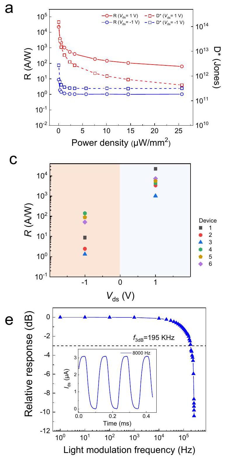
Responsivity-speed relations of device

To look into the responsivity-speed relations, we further analyze the optoelectrical properties of heterostructure devices under monochromatic light illuminations (see details in Supplementtary Note 9). According to the power-dependent photoresponse, the responsivities, , against power density are acquired at different (Fig. 3a). Notably, a high responsivity is obtained with ( ) when is applied, which is orders of magnitudes higher than that at . Similar enhancement at positive is also observed in multiple devices (Fig. 3c). The values are decreased with promoting light power at , and this phenomenon was generally attributed to the shortened photoinduced carrier lifetimes by Auger processes or by the saturation of trap states under a high photon flux . The device noise spectral densities is
b
d
f
Fig. 3 | The responsivity-speed relations of the heterostructure. a Extracted device responsivities, (solid lines), and detectivities, (dashed lines), at and 1 V , respectively. Extracted power dependence of the measured photocurrent at different . The solid lines are the exponential fitting between photocurrent and optical power. c Responsivity distribution of devices with different thicknesses. WSe : Device 1(D1): ; D2: ; D3: 35/ 23 nm ; D4: ; D5: ; D6: . The different shaded area indicates positive and negative bias conditions. d Response time of devices with different thicknesses. e Relative response with the modulation frequency
measured for Device 6. Inset: The time-dependent current of the device. The is defined as the laser modulation frequency when the photocurrent reduces to 0.707 of the maximum value. The performance comparison with previous reports (gray ellipsoid). Details of quoted references should refer to Supplementary Fig. 18. The heterostructures with different thicknesses are included. Among the devices that fulfill the 1 ms speed limit (The vertical dashed line) for imaging applications, our work shows both high responsivity, fast response and low power consumption.
derived from the time-resolved dark currents (Supplementary Note 11), and the corresponding specific detectivity results display similar trends as (Fig. 3a). In addition, by fitting the power-dependent photocurrents with a power-law relationship, (Fig. 3b), the is fitted to be 0.879 at , in stark contrast, the is 0.07 at , which means more traps or recombination centers participate in the photoresponse under positive than negative . According to previous reports, there is a trap-induced trade-off between responsivity and response speed (if photogating effect plays a dominant role) . However, in our device, this challenge is overcome with significant bias regulation, i.e., not only does the device
responsivity improves by three orders of magnitude when +1 V bias is applied compared to -1 V bias, the response speed also improves by an order of magnitude (Fig. 3c, d), simultaneously. These phenomena reveal that the speed constrains in defects-induced photogating effect is mitigated at positive
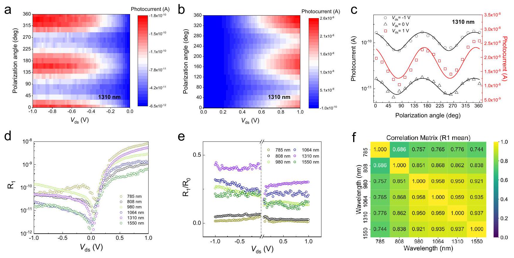
 . Similar phenomena were also found under the illumination of other wavelengths (e.g., 532 and 635 nm in Supplementary Note 10). Notably, the 3 dB cutoff frequency measured for the devices can reach a high value of at (Fig. 3e). The response time of the device is estimated to be by the equation: , where is the response time of the device, and the corresponding responsivity is at (details shown in
Fig. 4 | The photogating-empowered polarization photoresponse and wavelength discrimination in the heterostructure. Color plots of the polarization photocurrent under 1310 nm illumination at various bias voltages . The photoresponse of photodetector can be tuned by the and the incident light polarization angle, . c The polarization photocurrents under 1310 nm illumination. The photocurrent showcases the same dependency on polarization angle, , as sweeping from -1 V to 1 V . The solid lines are fits to the polarized photocurrent. d The extracted polarization sensitive contributions
( ) from the polarization photocurrents. depends on both the bias voltage and the incident light wavelength. e The anisotropic ratio , extracted from the polarization insensitive ( ) and sensitive ( ) contributions of the polarization photocurrent. The vertical dashed line indicates the two sectors being analyzed under positive and negative bias conditions. f The calculated correlation matrix between different wavelengths, with the element as the correlation coefficient of two columns of : , where and are two different wavelengths.
Supplementary Note 9). The bias tunability of our device provides a facile way to boost the device performance, and a target region that can overcome the responsivity-speed limit was reached with small power consumption (with measured values from 0.762 nW to 13 nW ) which is comparable to or even lower than the commercial photodetectors based on silicon, germanium and indium gallium arsenide (e.g. FDS1010, FD10D, DSD2 from Thorlabs), as illustrated in Fig. 3f (see more details in Supplementary Fig. 18).
Photogating-empowered polarized response under positive bias Since the number of the photoexcited-carriers in the is sensitive to polarization of incident light due to its in-plane anisotropic crystal structure, thereby, the light induced photogating at positive is polarization sensitive as well. The polarization-sensitive photogating will empower the device polarized light photodetection capability under positive even though the photocurrent is mainly generated at the metal/ Schottky junction. Besides, the relatively large bandgap of normally limits the device photoresponse to below . Nevertheless, in the above polarization-sensitive photogating process, the absorption of small-bandgap determines the operating wavelength range, which will surpass the limitation of photoresponse range of itself.
To verify the above analysis, we characterized our device at different illumination wavelengths in the infrared range up to 2200 nm (Supplementary Note 12). Considering the small bandgap of ( ), our device should also work at even longer wavelengths. The peak EQE reaches at 785 nm illumination and (Supplementary Note 13), and the EQE decreases to at 2200 nm wavelength.
In the following, we investigated the device polarization photoresponse under light illumination of different wavelengths. The schematic light path and measurement results are depicted in
Supplementary Fig. 22. The polarization angle is defined as the angle between light polarization and the metal electrode edge. The photocurrent varied periodically when the is rotated counterclockwise from to , and reached the maximum when light polarization is parallel to the elongated axis of , which is corresponding to the -axis of the flake. Further measurements reveal that the polarization photocurrent showcases the same dependency on crystal orientation as sweeping from -1 V to 1 V (Fig. ). The polarization dependent photocurrent can be described by a general formula: , with and representing the polarization insensitive and sensitive contributions, respectively. Once the two factors have been extracted, we can calculate the two widely used figure of merits in polarization photodetectors: the polarization ratio as | and the anisotropic ratio as . Notably, both the and are functions of applied source-drain bias and the wavelength of incident light, and , as shown in Fig. 4d, e. The polarization dependence is a result of the anisotropic structure of , in which the optical absorption coefficient along axis is calculated to be higher than that along axis for both mono- and multilayer (Supplementary Fig. 23). The calculated ratio of absorption coefficient along different crystalline orientations ( ) varies for different wavelengths and reaches the peak value around 1310 nm , accounting for the wavelength dependent and , in agreement with our experiments. Furthermore, the applied source-drain bias could alter the scattering of the photocarriers in the photogating process of our device so that the anisotropic response also becomes bias-tunable (Supplementary Note 14). The dependence of photoresponse on both bias and wavelength allows our device to discriminate different wavelengths by sweeping the bias. Figure 4 f shows the calculated correlation matrix between different wavelengths, with the element as the correlation coefficient of two columns of , where and
are two different wavelengths. It is worth noting that our method only requires two electrodes, a simple configuration for practical implementation of high-resolution pixels.

Discussion

In summary, we report a heterostructure with simultaneously improved responsivity and speed, with the aid of photogating-assisted carrier tunneling. The proposed mechanism helps achieve orders of magnitude faster carrier transit time, and shortened carrier lifetime by managing the trap sites, providing a state-of-the-art approach to address the trade-off between responsivity and speed in photodetectors based on photogating effect. Notably, the metal-induced gap state, external disorders/defects induced gap state or interface dipoles may lead to Fermi level pinning (FLP) effect at the metal contact interface . If fully de-pining is realized with van der Waals contacts , the device photoresponse could be further regulated by the gating effect. The observed wavelength-dependent polarization characteristics under positive biases validate that the photogating is polarization-sensitive. In the future work, the polarization photodetection in the infrared region could be further improved by coupling with plasmonic nanostructures or integrating with a circuitry amplification system, and we believe this has practical application for highly sensitive detection in multiple fields. Importantly, the tunable photoresponse of our device by switching source-drain voltages give us insight into the spectral information of incident lights, from which it is possible to reconstruct spectra from their corresponding photoresponse vectors by a unique spectral learning procedure in the future . Our results combine the physics of addressing the responsivity-speed trade-off and broadband polarized photodetection with wavelength discrimination, providing possibilities for exploring novel on-chip optoelectronic applications, such as in polarization imaging, high contrast polarizer, miniaturized spectrometer, etc.

Methods

Device fabrication

and nanosheets were fabricated via the mechanical exfoliation method from single crystals grown by the chemical vapor transport (CVT) method . Firstly, thin flakes of were exfoliated from its bulk crystals using scotch tape and then transferred onto a silicon substrate (with ). Then, multilayer were exfoliated onto the polydimethylsiloxane (PDMS) film and transferred selectively on top of the flake under the optical microscope assisted by an 3D positioning system. To fabricate the device for measurements, the source/drain electrodes were patterned by ultraviolet photolithography, and metals were deposited by the thermal evaporation.

Characterization of heterostructure

The morphologies of the heterostructure were investigated by an optical microscope (BX51, OLMPUS). The Raman mapping and PL mapping were carried out at room temperature by a confocal Raman/PL system (Alpha 300R, WITec) equipped with 532 and 633 nm laser sources. The thicknesses of the and nanoflakes were measured using atomic force microscopy (Cypher S, Asylum Research). The absorption spectra of the materials were measured using a customized microfocused absorption system.

Optoelectrical measurements

The electrical measurements were performed under ambient conditions at room temperature. All static behaviors of the photodetector were characterized by a semiconductor parameter analyzer (Keithley 4200) on a probe station (EVERBEING, C-4) in the dark and under illumination by different lasers: IR (2200, 1550, 1310, 1064, 980 and , red , green ( 532 nm ). The device has been measured multiple times to ensure the consistency of the dark current, and the
spot area of incident light was confirmed based on an optical microscope . The temporal responses of the device were recorded by a current meter after the light illumination switching on-off. The device 3 dB bandwidth is measured by modulating the laser switching frequency through a signal generator (RIGOL, DG822), and the modulated optical signal was focused on the photodetector through an optical microscope.

Photocurrent mapping

The spatial-resolved photocurrent mapping was conducted using scanning photocurrent microscopy built on a confocal Raman/PL system (WITec, Alpha 300R) with a high spatial resolution of about 350 nm . The device was laterally moved with steps of , where a focused laser beam ( ) was raster-scanned over the whole device area. The source-drain current was recorded by a current meter under various bias voltages .

Polarization-sensitive characterization

A linear polarizer (Thorlabs, LPVIS050) and half-wave plate were used to generate polarized light impinging on the sample in order to measure the polarization-dependent characteristics. The polarization angle was changed by rotating the polarizer.

DFT calculations

All calculations were performed with the Vienna ab initio simulation package . The projector augmented-wave (PAW) method was applied and the van der Waals interactions were considered by using DFT-D3 method . For the geometry optimization and electronic structure calculation with Perdew-Burke-Ernzerhof (PBE) functionals , the plane-wave cutoff energy is 500 eV and the k -point mesh for the first Brillouin zone is for both and heterostructures. A vacuum space of is set to avoid the interaction between the adjacent slabs. The convergence of force and total energy is and , respectively.
The optical absorption coefficient of is calculated by the following equation :
where and are the real and imaginary parts of the complex dielectric function, respectively. can be obtained from based on the Kramer-Kronig relationship.

Data availability

All technical details for producing the figures are enclosed in the supplementary information. Data are available from the corresponding authors D.L., C.-W.Q. or S.L. upon request.

References

  1. Sun, C. et al. Single-chip microprocessor that communicates directly using light. Nature 528, 534-538(2015).
  2. Elshaari, A. W., Pernice, W., Srinivasan, K., Benson, O. & Zwiller, V. Hybrid integrated quantum photonic circuits. Nat. Photon. 14, 285-298 (2020).
  3. Maiti, R. et al. Strain-engineered high-responsivity photodetector for silicon photonic integrated circuits. Nat. Photon. 14, 578-584 (2020).
  4. Yang, Z., Albrow-Owen, T., Cai, W. & Hasan, T. Miniaturization of optical spectrometers. Science 371, eabeO722 (2021).
  5. Xu, X. et al. Self-calibrating programmable photonic integrated circuits. Nat. Photon. 16, 595-602 (2022).
  6. Tian, R. et al. Chip-integrated van der Waals PN heterojunction photodetector with low dark current and high responsivity. Light Sci. Appl. 11, 101 (2022).
  7. Hui, Y., Gomez-Diaz, J. S., Qian, Z., Alù, A. & Rinaldi, M. Plasmonic piezoelectric nanomechanical resonator for spectrally selective infrared sensing. Nat. Commun. 7, 11249 (2016).
  8. Qian, Z. et al. Zero-power infrared digitizers based on plasmonically enhanced micromechanical photoswitches. Nat. Nanotechnol. 12, 969-973 (2017).
  9. Wei, J. et al. Zero-bias mid-infrared graphene photodetectors with bulk photoresponse and calibration-free polarization detection. Nat. Commun. 11, 6404 (2020).
  10. Bullock, J. et al. Polarization-resolved black phosphorus/molybdenum disulfide mid-wave infrared photodiodes with high detectivity at room temperature. Nat. Photon. 12, 601-607 (2018).
  11. Akinwande, D. et al. Graphene and two-dimensional materials for silicon technology. Nature 573, 507-518 (2019).
  12. Romagnoli, M. et al. Graphene-based integrated photonics for nextgeneration datacom and telecom. Nat. Rev. Mater. 3, 392-414 (2018).
  13. Zhang, Z. et al. All-in-one two-dimensional retinomorphic hardware device for motion detection and recognition. Nat. Nanotechnol. 17, 27-32 (2022).
  14. Lin, K.-T., Chen, H.-L., Lai, Y.-S. & Yu, C.-C. Silicon-based broadband antenna for high responsivity and polarization-insensitive photodetection at telecommunication wavelengths. Nat. Commun. 5, 3288 (2014).
  15. Lischke, S. et al. Ultra-fast germanium photodiode with 3-dB bandwidth of 265 GHz. Nat. Photon. 15, 925-931 (2021).
  16. Miyazaki, H. T. et al. Synchronously wired infrared antennas for resonant single-quantum-well photodetection up to room temperature. Nat. Commun. 11, 565 (2020).
  17. Novoselov, K. S., Mishchenko, A., Carvalho, A. & Castro Neto, A. H. 2D materials and van der Waals heterostructures. Science 353, aac9439 (2016).
  18. Guo, Z. et al. In-situ neutron-transmutation for substitutional doping in 2D layered indium selenide based phototransistor. eLight 2, 9 (2022).
  19. Lee, D. et al. Hyperbolic metamaterials: fusing artificial structures to natural 2D materials. eLight 2, 1 (2022).
  20. Konstantatos, G. et al. Hybrid graphene-quantum dot phototransistors with ultrahigh gain. Nat. Nanotechnol. 7, 363-368 (2012).
  21. Lopez-Sanchez, O., Lembke, D., Kayci, M., Radenovic, A. & Kis, A. Ultrasensitive photodetectors based on monolayer . Nat. Nanotechnol. 8, 497-501 (2013).
  22. Huo, N. & Konstantatos, G. Ultrasensitive all-2D MoS phototransistors enabled by an out-of-plane pn homojunction. Nat. Commun. 8, 572 (2017).
  23. Lee, S.-J. et al. Lead halide perovskite sensitized photodiodes with ultrahigh open circuit voltages. eLight 3, 8 (2023).
  24. Buscema, M. et al. Photocurrent generation with two-dimensional van der Waals semiconductors. Chem. Soc. Rev. 44, 3691-3718 (2015).
  25. Nikitskiy, I. et al. Integrating an electrically active colloidal quantum dot photodiode with a graphene phototransistor. Nat. Commun. 7, 11954 (2016).
  26. Ghosh, S., Varghese, A., Thakar, K., Dhara, S. & Lodha, S. Enhanced responsivity and detectivity of fast phototransistor using electrostatically tunable in-plane lateral p-n homojunction. Nat. Commun. 12, 3336 (2021).
  27. Flöry, N. et al. Waveguide-integrated van der Waals heterostructure photodetector at telecom wavelengths with high speed and high responsivity. Nat. Nanotechnol. 15, 118-124 (2020).
  28. Jiang, H. et al. Ultrasensitive and fast photoresponse in graphene/ silicon-on-insulator hybrid structure by manipulating the photogating effect. Nanophotonics 9, 3663-3672 (2020).
  29. Cao, G., Chen, G. & Li, X. Core-shell single-nanowire photodetector with radial carrier transport: an opportunity to break the
    responsivity-speed trade-off. Adv. Electron. Mater. 7, 2000920 (2021).
  30. Wang, C. et al. Integrated lithium niobate electro-optic modulators operating at CMOS-compatible voltages. Nature 562, 101-104 (2018).
  31. International technology roadmap for semiconductors. http:// www.itrs.net/.
  32. Wei, J., Xu, C., Dong, B., Qiu, C.-W. & Lee, C. Mid-infrared semimetal polarization detectors with configurable polarity transition. Nat. Photon. 15, 614-621 (2021).
  33. Ni, Y. et al. Computational spectropolarimetry with a tunable liquid crystal metasurface. eLight 2, 23 (2022).
  34. Nakano, A. et al. Antiferroelectric distortion with anomalous phonon softening in the excitonic insulator . Phys. Rev. B. 98, 045139 (2018).
  35. Di Salvo, F. J. et al. Physical and structural properties of the new layered compounds and . J. Less Common Met. 116, 51-61 (1986).
  36. Watson, M. D. et al. Band hybridization at the semimetalsemiconductor transition of enabled by mirror-symmetry breaking. Phys. Rev. Res. 2, 013236 (2020).
  37. Qiao, J. et al. Highly in-plane anisotropic two-dimensional ternary for polarization-sensitive photodetectors. ACS Appl. Mater. Interfaces 13, 17948-17956 (2021).
  38. Jog, H., Harnagea, L., Mele Eugene, J. & Agarwal, R. Exchange coupling-mediated broken symmetries in revealed from quadrupolar circular photogalvanic effect. Sci. Adv. 8, eabl9020 (2022).
  39. Lu, Y. F. et al. Zero-gap semiconductor to excitonic insulator transition in . Nat. Commun. 8, 14408 (2017).
  40. Qiao, J. et al. Perovskite quantum dot- mixed-dimensional van der Waals heterostructures for high-performance near-infrared photodetection. Adv. Funct. Mater. 32, 2110706 (2022).
  41. Zhou, H. et al. Large area growth and electrical properties of p-type atomic layers. Nano Lett. 15, 709-713 (2015).
  42. Jung, Y. et al. Transferred via contacts as a platform for ideal twodimensional transistors. Nat. Electron. 2, 187-194 (2019).
  43. Hong, . et al. Ultrafast charge transfer in atomically thin heterostructures. Nat. Nanotechnol. 9, 682-686 (2014).
  44. Li, L. et al. Ternary flakes for a high-performance infrared photodetector. Adv. Funct. Mater. 26, 8281-8289 (2016).
  45. Zhou, X. et al. Tunneling diode based on heterostructure incorporating high detectivity and responsivity. Adv. Mater. 30, 1703286 (2018).
  46. Liu, C.-H., Chang, Y.-C., Norris, T. B. & Zhong, Z. Graphene photodetectors with ultra-broadband and high responsivity at room temperature. Nat. Nanotechnol. 9, 273-278 (2014).
  47. Wang, Q. et al. Nonvolatile infrared memory in van der Waals heterostructures. Sci. Adv. 4, eaap7916 (2018).
  48. Mak, K. F., Lee, C., Hone, J., Shan, J. & Heinz, T. F. Atomically thin : a new direct-gap semiconductor. Phy. Rev. Lett. 105, 136805 (2010).
  49. Zhu, X., Li, F., Wang, Y., Qiao, M. & Li, Y. monolayer: a novel two-dimensional material with excellent electronic, transport, and optical properties. J. Mater. Chem. C. 6, 4494-4500 (2018).
  50. McDonnell, S. et al. Hole contacts on transition metal dichalcogenides: interface chemistry and band alignments. ACS Nano 8, 6265-6272 (2014).
  51. Nassiri Nazif, K. et al. High-specific-power flexible transition metal dichalcogenide solar cells. Nat. Commun. 12, 7034 (2021).
  52. Zhang, Y. et al. Ultra-broadband photodetection based on twodimensional layered with strong anisotropy and high responsivity. Mater. Des. 208, 109894 (2021).
  53. Tao, L., Chen, Z., Li, X., Yan, K. & Xu, J.-B. Hybrid graphene tunneling photoconductor with interface engineering towards fast photoresponse and high responsivity. npj 2D Mater. Appl. 1, 19 (2017).
  54. Wu, F. et al. AsP/InSe van der Waals tunneling heterojunctions with ultrahigh reverse rectification ratio and high photosensitivity. Adv. Funct. Mater. 29, 1900314 (2019).
  55. Sze, S. M., Li, Y., Ng, K. K. Physics of semiconductor devices (John Wiley & Sons, 2021).
  56. Seeger K. Semiconductor physics (Springer Science & Business Media, 2013).
  57. Koppens, F. H. L. et al. Photodetectors based on graphene, other two-dimensional materials and hybrid systems. Nat. Nanotechnol. 9, 780-793 (2014).
  58. Feng, S. et al. An ultrasensitive molybdenum-based double-heterojunction phototransistor. Nat. Commun. 12, 4094 (2021).
  59. Liu, Y., Stradins, P., Wei, S.-H. Van der Waals metal-semiconductor junction: weak Fermi level pinning enables effective tuning of Schottky barrier. Sci. Adv. 2, e1600069 (2016).
  60. Kong, L. et al. Doping-free complementary circuit via van der Waals metal integration. Nat. Commun. 11, 1866 (2020).
  61. Yang, Z. et al. Single-nanowire spectrometers. Science 365, 1017-1020 (2019).
  62. Yuan, S., Naveh, D., Watanabe, K., Taniguchi, T. & Xia, F. A wavelength-scale black phosphorus spectrometer. Nat. Photon. 15, 601-607 (2021).
  63. Ma, C. et al. Intelligent infrared sensing enabled by tunable moiré quantum geometry. Nature 604, 266-272 (2022).
  64. Wang, F., Zhang, T., Xie, R., Wang, Z. & Hu, W. How to characterize figures of merit of two-dimensional photodetectors. Nat. Commun. 14, 2224 (2023).
  65. Kresse, G. & Joubert, D. From ultrasoft pseudopotentials to the projector augmented-wave method. Phys. Rev. B. 59, 1758-1775 (1999).
  66. Grimme, S., Antony, J., Ehrlich, S. & Krieg, H. A consistent and accurate ab initio parametrization of density functional dispersion correction (DFT-D) for the 94 elements H-Pu. J. Chem. Phys. 132, 154104 (2010).
  67. Perdew, J. P., Burke, K. & Ernzerhof, M. Generalized gradient approximation made simple. Phy. Rev. Lett. 78, 1396-1396 (1997).
  68. Fox, M. Optical properties of solids. Am. J. Phys. 70, 1269-1270 (2002).

Acknowledgements

S.L. acknowledges the financial support from the National Natural Science Foundation of China (No. 62121005, 62022081, 62334010 and 61974099), the National Key Research and Development Program (2021YFA0717600), the Natural Science Foundation of Jilin Province (20210101173JC) and Changchun Key Research and Development Program (21ZYO3). K.S.N. is grateful to the Ministry of Education, Singapore (Research Centre of Excellence award to the Institute for Functional Intelligent Materials, I-FIM, project No. EDUNC-33-18-279-V12) and Royal
Society (UK, grant 304 number RSRPR190000) for support. C.-W.Q. acknowledges financial support from the National Research Foundation (Grant No. NRF-CRP26-2021-0004).

Author contributions

S.L., C.-W.Q. and D.L. conceived of the original concept and supervised the project. M.L., J.W. and S.L. performed most of the experiments. L.Q. and Z.S. contributed to the computational theoretical analysis. M.L. and Y.L. contributed to material preparations and characterizations. M.L. and Y.L. contributed to the photoresponse measurements. M.L., J.W., L.Q., J.A., X.L., Y.L., Z.S., K.S.N., D.L. and S.L. analyzed the data and co-wrote the paper. All authors discussed the results and commented on the manuscript. All authors have approved the final version of the manuscript.

Competing interests

The authors declare no competing interests.

Additional information

Supplementary information The online version contains
supplementary material available at
https://doi.org/10.1038/s41467-023-44482-7.
Correspondence and requests for materials should be addressed to Dabing Li, Cheng-Wei Qiu or Shaojuan Li.
Peer review information Nature Communications thanks Jian-Bin Xu and the other, anonymous, reviewers for their contribution to the peer review of this work. A peer review file is available.
Reprints and permissions information is available at
http://www.nature.com/reprints
Publisher’s note Springer Nature remains neutral with regard to jurisdictional claims in published maps and institutional affiliations.
Open Access This article is licensed under a Creative Commons Attribution 4.0 International License, which permits use, sharing, adaptation, distribution and reproduction in any medium or format, as long as you give appropriate credit to the original author(s) and the source, provide a link to the Creative Commons license, and indicate if changes were made. The images or other third party material in this article are included in the article’s Creative Commons license, unless indicated otherwise in a credit line to the material. If material is not included in the article’s Creative Commons license and your intended use is not permitted by statutory regulation or exceeds the permitted use, you will need to obtain permission directly from the copyright holder. To view a copy of this license, visit http://creativecommons.org/ licenses/by/4.0/.
© The Author(s) 2024

  1. State Key Laboratory of Luminescence and Applications, Changchun Institute of Optics, Fine Mechanics and Physics, Chinese Academy of Sciences, Jilin 130033 Changchun, PR China. University of Chinese Academy of Sciences (UCAS), 100049 Beijing, PR China. Department of Electrical and Computer Engineering, National University of Singapore, Singapore 117583, Singapore. School of Optoelectronic Science and Engineering, University of Electronic Science and Technology of China, 611731 Chengdu, PR China. Institute for Functional Intelligent Materials, National University of Singapore, Singapore 117544, Singapore. These authors contributed equally: Mingxiu Liu, Jingxuan Wei, Liujian Qi. e-mail: lidb@ciomp.ac.cn; chengwei.qiu@nus.edu.sg; lishaojuan@ciomp.ac.cn