تنفيذ الأجهزة لشبكات عصبية اصطناعية تعتمد على الميمريستور Hardware implementation of memristor-based artificial neural networks

المجلة: Nature Communications، المجلد: 15، العدد: 1
DOI: https://doi.org/10.1038/s41467-024-45670-9
PMID: https://pubmed.ncbi.nlm.nih.gov/38438350
تاريخ النشر: 2024-03-04

تنفيذ الأجهزة لشبكات عصبية اصطناعية تعتمد على الميمريستور

تاريخ الاستلام: 8 يونيو 2023
تم القبول: 1 فبراير 2024
نُشر على الإنترنت: 04 مارس 2024
(د) التحقق من التحديثات

الملخص

فرناندو أغيري أبو سباستيان © مانويل لو غالو © وينهاو سونغ تونغ وانغ ج. جوشوا يانغ وي لو منغ-فان تشانغ دانييل إيلميني يوتشاو يانغ © عدنان ميهوني © أنتوني كينيون © ماركو أ. فيلينا © خوان ب. رولدان © يوتينغ وو هونغ-شي هسو ناغاراجان راغافان جوردي سوني © إنريكي ميراندا أحمد التويل © جيانلوكا سيتّي كاميلية سماغولوفا خالد ن. سلامة © أولغا كريستينسكايا © شياوبينغ يان © كا-وي أنغ سامارث جاين سيفان لي أسامة الحربي © سباستيان بازوس © وماريو لانسو ©

الملخص

تجرب الذكاء الاصطناعي (AI) حاليًا ازدهارًا مدفوعًا بتقنيات التعلم العميق (DL)، التي تعتمد على شبكات من وحدات حساب بسيطة متصلة تعمل بالتوازي. إن عرض النطاق الترددي المنخفض بين الذاكرة ووحدات المعالجة في آلات فون نيومان التقليدية لا يدعم متطلبات التطبيقات الناشئة التي تعتمد بشكل كبير على مجموعات كبيرة من البيانات. تساعد نماذج الحوسبة الأكثر حداثة، مثل التوازي العالي والحوسبة القريبة من الذاكرة، في تخفيف عنق الزجاجة في الاتصال بالبيانات إلى حد ما، ولكن هناك حاجة إلى مفاهيم تحولية. تعتبر الميمريستورز، وهي تقنية جديدة تتجاوز أشباه الموصلات المعدنية-أكسيد-المكمل (CMOS)، خيارًا واعدًا لأجهزة الذاكرة نظرًا لخصائصها الفريدة على مستوى الجهاز، مما يمكّن من التخزين والحوسبة مع بصمة صغيرة ومتوازية بشكل كبير وبطاقة منخفضة. نظريًا، يترجم هذا مباشرة إلى زيادة كبيرة في كفاءة الطاقة ومعدل الأداء الحاسوبي، ولكن لا تزال هناك تحديات عملية متنوعة. في هذا العمل، نستعرض أحدث الجهود لتحقيق الشبكات العصبية الاصطناعية (ANNs) القائمة على الميمريستور، موضحين بالتفصيل مبادئ العمل لكل كتلة والبدائل التصميمية المختلفة مع مزاياها وعيوبها، بالإضافة إلى الأدوات المطلوبة للتقدير الدقيق لمقاييس الأداء. في النهاية، نهدف إلى تقديم بروتوكول شامل للمواد والأساليب المعنية في الشبكات العصبية الميمريستورية لأولئك الذين يهدفون إلى البدء في العمل في هذا المجال والخبراء الذين يبحثون عن نهج شامل.

أصبح تطوير الشبكات العصبية الاصطناعية المتطورة (ANNs) واحدة من أعلى أولويات الشركات التكنولوجية وحكومات الدول الغنية، حيث يمكن أن تعزز من تصنيع أنظمة الذكاء الاصطناعي (AI) التي تولد فوائد اقتصادية واجتماعية في مجالات متعددة (مثل، اللوجستيات، التجارة، الرعاية الصحية،
الأمن القومي، إلخ. تستطيع الشبكات العصبية الاصطناعية حساب وتخزين الكمية الهائلة من البيانات الإلكترونية المنتجة (سواء من قبل البشر أو الآلات)، وتنفيذ عمليات معقدة بها. من أمثلة المنتجات الإلكترونية التي تحتوي على شبكات عصبية اصطناعية نتفاعل معها في حياتنا اليومية هي تلك التي تحدد الأنماط البيومترية (مثل الوجه، بصمة الإصبع) للوصول.
التحكم في الهواتف الذكية أو تطبيقات الخدمات المصرفية عبر الإنترنت ، وتلك التي تحدد الكائنات في الصور من الشبكات الاجتماعية وكاميرات الأمن/المرور بجانب التعرف على الصور، هناك أمثلة أخرى مثل المحركات التي تحول الكلام إلى نص في الحواسيب والهواتف الذكية. معالجة اللغة الطبيعية مثل نظام الدردشة الآلي الجديد chat-GPT وتلك التي تقدم توصيات دقيقة للتسوق عبر الإنترنت بناءً على سلوكيات سابقة من أنفسنا و/أو من الأشخاص في شبكتنا .
يمكن فهم الشبكات العصبية الاصطناعية على أنها تنفيذ سلسلة من العمليات الرياضية. تتكون بنية الشبكات العصبية الاصطناعية من عدة عقد (تسمى الخلايا العصبية) مترابطة مع بعضها البعض (عن طريق المشابك)، ويتم تنفيذ التعلم من خلال ضبط قوة (وزن) هذه الاتصالات. يتم تنفيذ الشبكات العصبية الاصطناعية الحديثة عبر البرمجيات في أنظمة الحوسبة العامة المستندة إلى وحدة المعالجة المركزية (CPU) والذاكرة – المعمارية المعروفة باسم فون نيومان. . ومع ذلك، في هذه البنية، يرتبط مقدار كبير من استهلاك الطاقة ووقت الحوسبة بتبادل البيانات المستمر بين الوحدتين، وهو ما ليس بكفاءة. يمكن تسريع وقت الحوسبة عن طريق
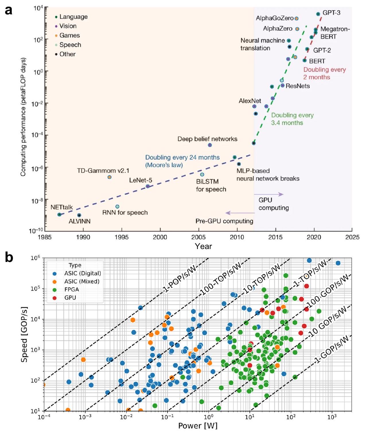
استخدام وحدات معالجة الرسوميات (GPUs) لتنفيذ الشبكات العصبية الاصطناعية (انظر الشكل 1أ)، حيث يمكنها تنفيذ عمليات متعددة بشكل متوازي . ومع ذلك، فإن هذا النهج يستهلك المزيد من الطاقة، مما يتطلب أنظمة حوسبة كبيرة وبالتالي لا يمكن دمجه في الأجهزة المحمولة. خيار آخر هو استخدام مصفوفات البوابات القابلة للبرمجة في الميدان (FPGAs)، التي تستهلك طاقة أقل بكثير من وحدات معالجة الرسوميات (GPUs) بينما توفر كفاءة حوسبة متوسطة بين وحدات المعالجة المركزية (CPUs) ووحدات معالجة الرسوميات. استطلاع أجرته غوان وآخرون تم تلخيص الحلول الحالية للأجهزة لتنفيذ الشبكات العصبية الاصطناعية وأدائها في الشكل 1b.
في السنوات القليلة الماضية، قدمت بعض الشركات والجامعات دوائر متكاملة محددة التطبيقات (ASICs) تعتمد على تقنية أشباه الموصلات المعدنية المؤكسدة التكميلية (CMOS) القادرة على حساب وتخزين المعلومات في نفس الوحدة. وهذا يسمح لهذه الدوائر المتكاملة بأداء عمليات متعددة بشكل متوازي وبسرعة كبيرة، مما يجعلها قادرة على تقليد سلوك الخلايا العصبية والوصلات العصبية في الشبكات العصبية الاصطناعية (ANN) مباشرة في الأجهزة. قائمة شاملة من هذه الدوائر المتكاملة تشمل تلك مثل وحدة معالجة جوجل (TPU). أمازون إنفيرنتيا تسلا NPU ، إلخ، ملخصة في المرجع 22. مثل هذه المتكاملة
الشكل 1 | زيادة الطلب على قوة الحوسبة وانتقال المنصة من فون نيومان نحو الهياكل المعالجة بشكل متوازي. أ زيادة الطلب على قوة الحوسبة على مدى العقود الأربعة الماضية معبرًا عنها بوحدات بيتا فلوپس في اليوم. حتى عام 2012، كان الطلب على قوة الحوسبة يتضاعف كل 24 شهرًا؛ مؤخرًا، تم تقصير هذه الفترة إلى حوالي كل شهرين. تشير أسطورة الألوان إلى اختلافات
مجالات التطبيق ميهونيك، أ.، كينون، أ. ج. الحوسبة المستوحاة من الدماغ تحتاج إلى خطة رئيسية. ناتشر 604، 255-260 (2022)، معاد إنتاجها بإذن من SNCSC. ب مقارنة لمسرعات الشبكات العصبية لأجهزة FPGA وASIC وGPU من حيث السرعة واستهلاك الطاقة. GOP/s عمليات جيجا في الثانية، تيرا عمليات في الثانية.
يمكن تصنيف الدوائر إلى فئتين. من ناحية، تعتبر معالجات تدفق البيانات معالجات مصممة خصيصًا لاستنتاج وتدريب الشبكات العصبية. نظرًا لأن حسابات تدريب واستنتاج الشبكات العصبية يمكن أن تُرتب بشكل حتمي تمامًا، فهي قابلة لمعالجة تدفق البيانات حيث يتم برمجة أو وضع وتوجيه الحسابات، والوصول إلى الذاكرة، وإجراءات الاتصالات بين وحدات المعالجة الحسابية بشكل صريح/ثابت على الأجهزة الحاسوبية. من ناحية أخرى، تدمج معجلات المعالجة في الذاكرة (PIM) عناصر المعالجة مع تكنولوجيا الذاكرة. من بين هذه المعجلات PIM توجد تلك المعتمدة على تكنولوجيا الحوسبة التناظرية التي تعزز دوائر الذاكرة الفلاش بقدرات الجمع والضرب التناظرية في المكان. يرجى الرجوع إلى المراجع الخاصة بـ Mythic. والصقر الجير مسرعات لمزيد من التفاصيل حول هذه التكنولوجيا المبتكرة.
الشبكات العصبية الاصطناعية المذكورة سابقًا وتلك التي تم الإبلاغ عنها بالتفصيل في الاستطلاع المقدم في المرجع 22 تنتمي إلى مجموعة فرعية تُعرف بالشبكات العصبية العميقة (DNNs). في الشبكة العصبية العميقة، يتم تمثيل المعلومات بقيم مستمرة في الزمن ويمكن أن تحقق دقة عالية في التعرف على البيانات من خلال استخدام طبقتين على الأقل من الخلايا العصبية غير الخطية المترابطة بواسطة أوزان تشابكية قابلة للتعديل. . على العكس من ذلك، هناك ترميز بديل للمعلومات أدى إلى ظهور نوع آخر من الشبكات العصبية الاصطناعية، وهي الشبكات العصبية النابضة (SNN). في الشبكات العصبية النابضة، يتم ترميز المعلومات بواسطة نبضات تعتمد على الزمن، مما يقلل بشكل ملحوظ من استهلاك الطاقة مقارنة بالشبكات العصبية العميقة (DNN). علاوة على ذلك، فإن وظيفة الشبكات العصبية السريعة (SNNs) تشبه بشكل أكبر الوظيفة الفعلية للشبكات العصبية البيولوجية، ويمكن أن تساعد في فهم الأنظمة العصبية المعقدة للثدييات. من المحتمل أن تكون إنتل لديها أكثر برامج البحث شمولاً لتقييم الجدوى التجارية لمسرعات SNN بتقنيتها لوهي. ومجتمع تطوير الذكاء العصبي من إنتل . من بين التطبيقات التي تم استكشافها مع لوهي هي تصنيف الأهداف في رادار الفتحة الاصطناعية والصور البصرية , تحليل مشهد السيارات , ومشفّر الطيف . علاوة على ذلك، أعلنت شركة واحدة، إيناتيرا، عن معالج SNN تجاري . أيضًا، المنصات التي طورتها IBM (TrueNorth )، وتسينغوا هي أمثلة معروفة على جهود البحث من كل من الصناعة والأكاديمية في هذا المجال.
ومع ذلك، تتطلب تطبيقات ANNs المعتمدة على CMOS بالكامل عشرات الأجهزة لمحاكاة كل مشبك عصبي، مما يهدد كفاءة الطاقة والمساحة، وبالتالي يجعل الأنظمة الكبيرة الحجم غير عملية. نتيجة لذلك، لا يزال أداء ANNs المعتمدة على CMOS بعيدًا جدًا عن أداء الشبكات العصبية البيولوجية. لمحاكاة التعقيد واستهلاك الطاقة المنخفض للغاية للشبكات العصبية البيولوجية، يجب أن تحقق المنصات المادية لـ ANNs كثافة تكامل عالية جدًا ( تيرابايت لكل ) واستهلاك طاقة منخفض ( لكل عملية .
أشارت الدراسات الحديثة إلى أن استخدام الأجهزة الميمريستية لمحاكاة المشابك العصبية قد يسرع من مهام حساب ANNs مع تقليل استهلاك الطاقة العام والبصمة . الأجهزة الميمريستية هي أنظمة مواد يمكن ضبط مقاومتها الكهربائية على حالتين ثابتتين أو أكثر (أي غير متطايرة) عن طريق تطبيق ضغوط كهربائية . الأجهزة الميمريستية التي تظهر حالتين غير متطايرتين يتم تسويقها بالفعل كذاكرة مستقلة , على الرغم من أن سوقها العالمي لا يزال صغيرًا ( مليون دولار أمريكي بحلول عام 2020، أي من سوق الذاكرة المستقلة الذي تبلغ قيمته 127 مليار ). ومع ذلك، يمكن أن تظهر الأجهزة الميمريستية أيضًا ثلاث سمات مدمرة مناسبة بشكل خاص للتنفيذ المادي لـ ANNs: i) إمكانية برمجة حالات غير متطايرة متعددة (حتى ، وحتى )، ii) استهلاك طاقة منخفض للتبديل ( لكل انتقال حالة مع استهلاك ثابت صفر عند الخمول )، و iii) هيكل قابل للتوسع مناسب للتكامل المصفوفي (غالبًا ما يُشار إليه باسم تقاطع ) وحتى التكديس ثلاثي الأبعاد . علاوة على ذلك، يمكن أن يكون وقت التبديل قصيرًا يصل إلى .
حتى الآن، ادعت عدة مجموعات وشركات تحقيق تنفيذات هجينة من ANNs المعتمدة على CMOS/ميمريستور , -من الآن فصاعدًا، ANNs الميمريستية- بأداء يتفوق على نظيراتها المعتمدة على CMOS بالكامل. ومع ذلك، فإن معظم تلك الدراسات في الواقع قاست فقط أرقام الجدارة لواحد/قليل من الأجهزة ومحاكاة
دقة ANN عبر البرمجيات في هذا النوع من الدراسات، تكون العلاقة بين الميمريستورات المصنعة وANN ضعيفة نسبيًا. ذهبت بعض الدراسات إلى ما هو أبعد من ذلك وبنت/وصفت مصفوفات تقاطع من الأجهزة الميمريستية , لكنها لا تزال بعيدة جدًا عن تنفيذات الأجهزة الكاملة لجميع العمليات الرياضية المطلوبة من قبل ANN. أفادت الدراسات الأكثر تقدمًا في هذا المجال بأنظمة حساب في الذاكرة تعتمد على الميمريستور متكاملة بالكامل , لكن الوصف المنهجي للتفاصيل الأساسية حول هيكل الجهاز أو بنية الدائرة غالبًا ما يكون مفقودًا في هذه التقارير.
في هذه المقالة نقدم وصفًا شاملًا خطوة بخطوة لتنفيذ الأجهزة لـ ANNs الميمريستية لتصنيف الصور -التطبيق الأكثر دراسة والذي غالبًا ما يستخدم لتقييم الأداء، موضحين جميع الكتل الأساسية اللازمة وتدفق معالجة المعلومات. من أجل الوضوح، نعتبر الشبكات البسيطة نسبيًا، حيث تكون الشبكة متعددة الطبقات هي الحالة الأكثر تعقيدًا. نأخذ في الاعتبار التحديات التي تنشأ على كل من مستوى الجهاز والدائرة ونناقش نهجًا قائمًا على SPICE لدراستها في مرحلة التصميم، بالإضافة إلى التوبولوجيات الدائرية المطلوبة لتصنيع ANN ميمريستية.

هيكل ANNs المعتمدة على الميمريستور

تظهر الشكل 2 مخطط تدفق يوضح الهيكل العام لـ ANN؛ يحتوي على مدخلات متعددة (لصور القناة الواحدة مثل الألوان المفهرسة، الصور الرمادية وصور البت، هناك عدد من المدخلات بقدر عدد البكسلات التي تحتويها الصورة المراد تصنيفها) وعدة مخرجات (بقدر أنواع/فئات الصور التي سيتعرف عليها ANN). كما يتضح، يتكون ANN من عمليات رياضية متعددة (صناديق خضراء)، مثل ضرب مصفوفة المتجهات (VMM)، دالة التنشيط، ودالة softargmax. من بين جميع العمليات الحرجة في ANN، تعتبر VMM الأكثر تعقيدًا ومتطلبات، ويتم تنفيذها عدة مرات خلال عملية التدريب والاستدلال. وبالتالي، فإن تطوير أجهزة جديدة لتنفيذ ANN موجه بقوة لتحقيق عمليات VMM بطريقة أكثر كفاءة. من المثير للاهتمام، أن عملية VMM -التي غالبًا ما تُفهم على أنها روتين الضرب والتجميع (MAC)- يمكن تنفيذها باستخدام مصفوفة تقاطع من عناصر الذاكرة. يمكن أن تكون تلك الأجهزة الذاكرية إما ذاكرات قائمة على الشحن أو ذاكرات قائمة على المقاومة .
قبل شرح الأجهزة الميمريستية لـ ANN، في هذه الفقرة نصف حالة الفن للأجهزة CMOS لـ ANNs، لتزويد المؤلف بصورة شاملة عن التقنيات المختلفة المتاحة لـ ANNs المعتمدة على الأجهزة. من بين الذاكرات القائمة على الشحن، تم استخدام خلايا SRAM (هيكل ترانزستور ثنائي الاستقرار مصنوع عادةً من اثنين من المحولات CMOS متصلة ببعضها البعض والتي تحتفظ بتركيز الشحن، انظر الشكل 3a كمثال على هيكل مصفوفة تقاطع من 6T SRAM) على نطاق واسع لـ VMM . إذا كانت عناصر متجه الإدخال ومصفوفة الوزن محدودة بالقيم الثنائية الموقعة، فإن عملية الضرب تُبسط إلى مجموعة من وظائف XNOR وADD التي يتم تنفيذها مباشرة من خلال خلايا SRAM. مثال على ذلك هو العمل الذي قام به خوا وآخرون، الذي يذكر نظام حساب في الذاكرة يعتمد على مصفوفة تقاطع من خلايا ذاكرة 6T SRAM كاتصالات مشبكية ثنائية تستخدم مدخلات/مخرجات ثنائية . الدائرة المقترحة تتكون من 4 كيلوبايت من المشابك المصنعة في عملية CMOS 65 نانومتر وأبلغت عن كفاءة طاقة تبلغ 55.8 TOPS لكل واط. في الحالات التي تكون فيها x غير ثنائية، تتمثل إحدى الطرق في استخدام المكثفات بالإضافة إلى خلايا SRAM , مما ينطوي على عملية من ثلاث خطوات. ومع ذلك، فإن العيب الرئيسي لذاكرات SRAM هو طبيعتها المتطايرة. بسبب ارتفاع حاجز ترانزستور التأثير الميداني المنخفض ( 0.5 eV )، يحتاج الشحن باستمرار إلى التجديد من مصدر خارجي ومن ثم تحتاج SRAM دائمًا إلى الاتصال بمصدر طاقة. عنصر ذاكرة بديل لعملية VMM هو خلية الذاكرة الفلاش , حيث يتم ربط عقدة تخزين الشحن ببوابة FET مع الشحن المخزن إما على قطب موصل محاط بالعوازل (البوابة العائمة) أو في فخاخ منفصلة داخل طبقة عازل معيبة (طبقة حبس الشحن). على عكس SRAM، فإن ارتفاع الحاجز لـ
الشكل 2 | مخطط كتلي عام يشير إلى الكتل الدائرية المطلوبة لتنفيذ ANN ميمريستية لتصنيف الأنماط. تشير الكتل الخضراء (3،5،7 و8) إلى العمليات الرياضية المطلوبة (مثل VMM أو دوال التنشيط). تحدد الكتل الحمراء الدوائر المطلوبة لتكييف الإشارة و/أو تحويلها. يتم الإشارة إلى مسار البيانات المتبع أثناء الاستدلال (أو المرور الأمامي) بواسطة الأسهم/الخطوط الحمراء. يتم الإشارة إلى مسار البيانات المتبع للتدريب في الموقع بواسطة الأسهم/الخطوط الزرقاء. يتم الإشارة إلى مسار البيانات المتبع
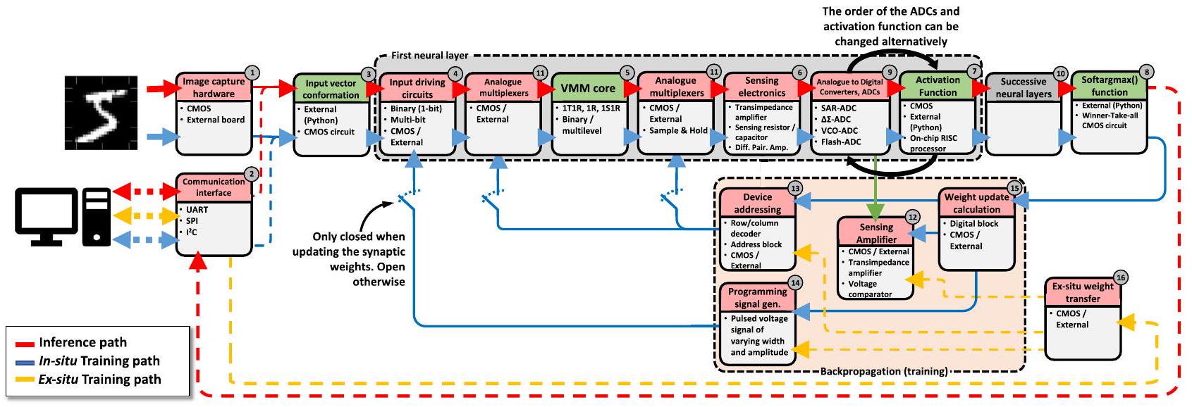
خلال التدريب خارج الموقع بواسطة الأسهم/الخطوط الصفراء. لكل صندوق، تشير الجزء العلوي (المُلوّن) إلى اسم الوظيفة التي يجب تحقيقها بواسطة الكتلة الدائرية، والجزء السفلي يشير إلى نوع الأجهزة المطلوبة. يشمل الصندوق المعنون بالطبقات العصبية المتعاقبة عدة كتل فرعية بهيكل مشابه للمجموعة المعنونة بالطبقة العصبية الأولى. 1S1R تعني 1 محدد 1 مقاوم بينما 1R تعني 1 مقاوم. UART وSPI و هي معايير اتصالات معروفة. RISC تعني جهاز كمبيوتر مجموعة التعليمات المخفضة.
ارتفاع عقدة التخزين مرتفع بما يكفي للاحتفاظ بالبيانات على المدى الطويل. أيضًا، تعمل VMM المعتمدة على الفلاش بطريقة مختلفة قليلاً عن VMM المعتمدة على SRAM. في VMM المعتمدة على الفلاش، يساهم كل عنصر ذاكرة بمقدار مختلف في التيار في كل عمود من مصفوفة التقاطع اعتمادًا على الجهد المطبق على المدخل أو صف التقاطع وعناصر المصفوفة مخزنة كشحن على البوابة العائمة (أي، الضرب) وجميع التيارات في عمود ما يتم جمعها على الفور (أي، التراكم) بواسطة قانون كيرشوف للتيارات. نظرًا لأن الأجهزة يمكن الوصول إليها بالتوازي على طول BL، فإن ذاكرة فلاش NOR تُفضل عمومًا على ذاكرة فلاش NAND للحوسبة في الذاكرة. هذه هي حالة العمل الذي قام به فيك وآخرون من شركة ميثيك ، الذي يعتمد على مصفوفة فلاش NOR لتطوير معالج مصفوفة تناظرية لاكتشاف وضع الإنسان في معالجة الفيديو في الوقت الحقيقي. ومع ذلك، هناك عمل حديث يصف استخدام NAND ثلاثي الأبعاد، المكون من طبقات مكدسة عموديًا من أجهزة فلاش المتصلة تسلسليًا، حيث تقوم كل طبقة من المصفوفة بتشفير مصفوفة فريدة . يمكن أن تساعد هذه الطريقة في التغلب على مشكلة قابلية التوسع لذاكرة فلاش NOR، والتي يصعب توسيعها إلى ما بعد عقدة تكنولوجيا 28 نانومتر. المسرع المقترح 3D-aCortex هو تنفيذ كامل بتقنية CMOS يعتمد على مصفوفة فلاش NAND ثلاثية الأبعاد تجارية كعنصر تشابكي. يتم تجميع المخرجات الجزئية من عدة مصفوفات تشابكية مؤقتًا ورقميًا باستخدام عدادات رقمية، مشتركة بين جميع المصافي على طول صف من الشبكة، مما يتجنب عبء الاتصال الناتج عن إجراء هذه التخفيضات عبر مستويات متعددة من التسلسل الهرمي. تشارك المصفوفة ثلاثية الأبعاد بأكملها ذاكرة عالمية وعمود من الدوائر المحيطية، مما يزيد من كفاءة تخزينها. ومع ذلك، لا يزال هذا نظريًا ولم يتم تصنيعه بعد. ومع ذلك، تتطلب عملية الكتابة على ذاكرات الفلاش فولتages عالية (عادةً ) وتنطوي على زمن تأخير كبير ( ) بسبب الحاجة إلى التغلب على حواجز عقد التخزين. يمكن حل هذه المشكلات بشكل محتمل باستخدام ذاكرات قائمة على المقاومة، أو الميمريستور كعنصر ذاكرة عند تقاطعات المصفوفة، حيث يمكنها تحقيق عملية الضرب بموجب قانون أوم ( ، حيث هو التيار، هو جهد الإدخال و هو موصلية كل ميمريستور)، مع تقليل استهلاك الطاقة والمساحة بالإضافة إلى توفير فولتages تشغيل متوافقة مع CMOS. يتم تصوير هيكل مصفوفات الميمريستور التشابكية لـ VMM في الشكل 3b، c: خيار التكامل الشائع هو وضع ترانزستور CMOS في سلسلة مع الميمريستور للتحكم في التيار من خلاله (الشكل 3b) في هيكل يسمى 1 ترانزستور 1 مقاومة (1T1R)، بينما سيتم تحقيق أعلى كثافة تكامل من خلال مصفوفة تشابكية لا تحتوي على ترانزستورات، أي، اعتبار الخلايا التي يشار إليها عادةً باسم 1 مقاومة/
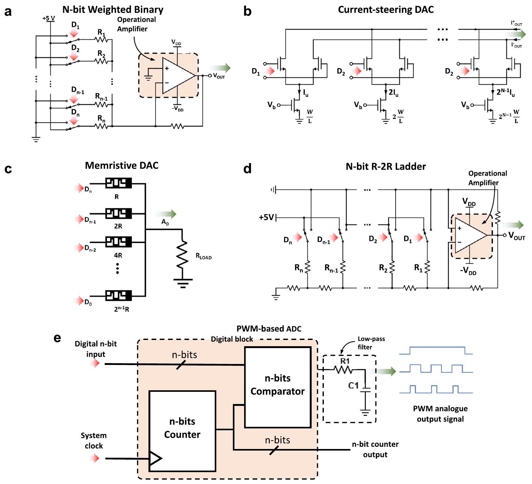
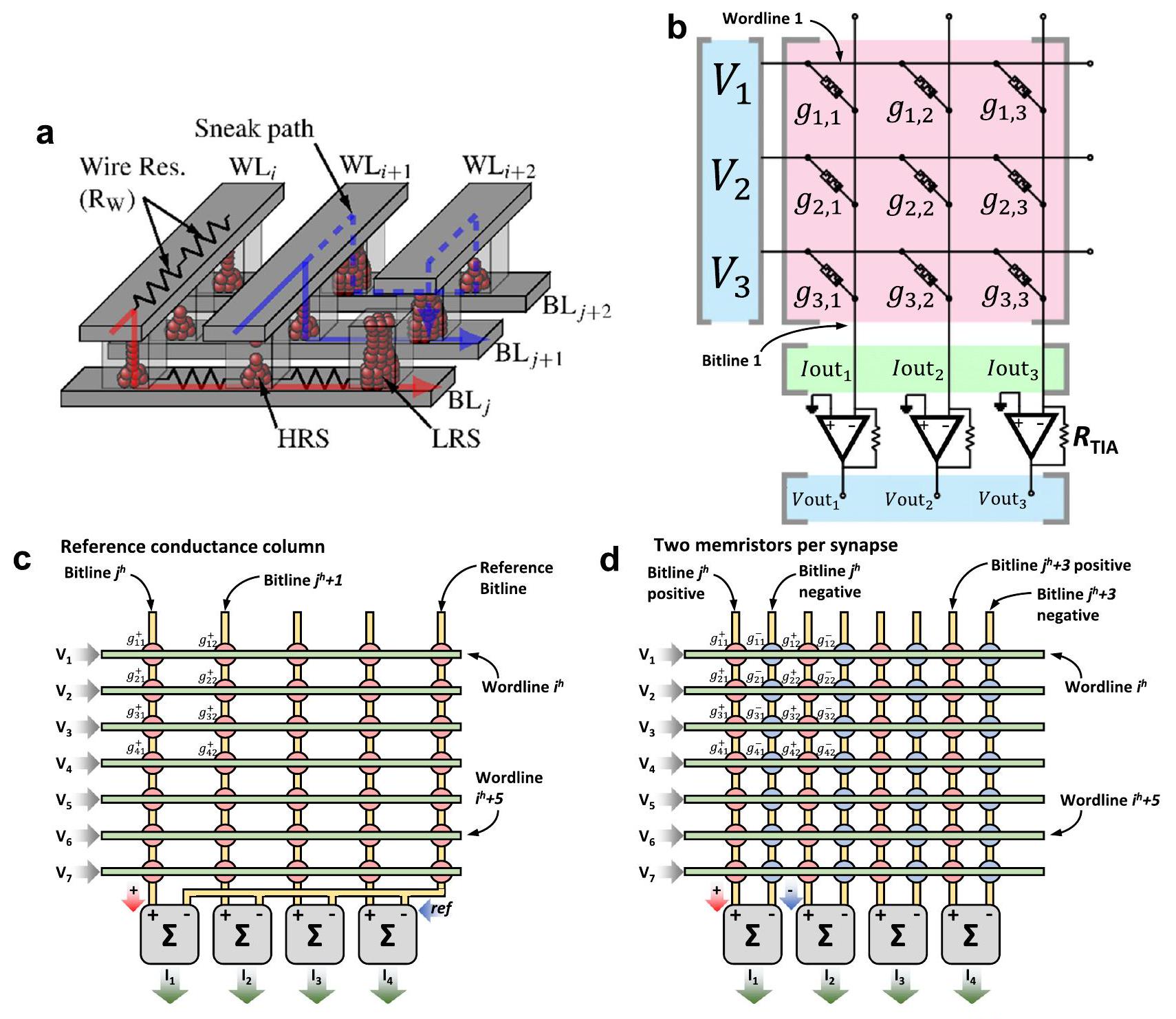
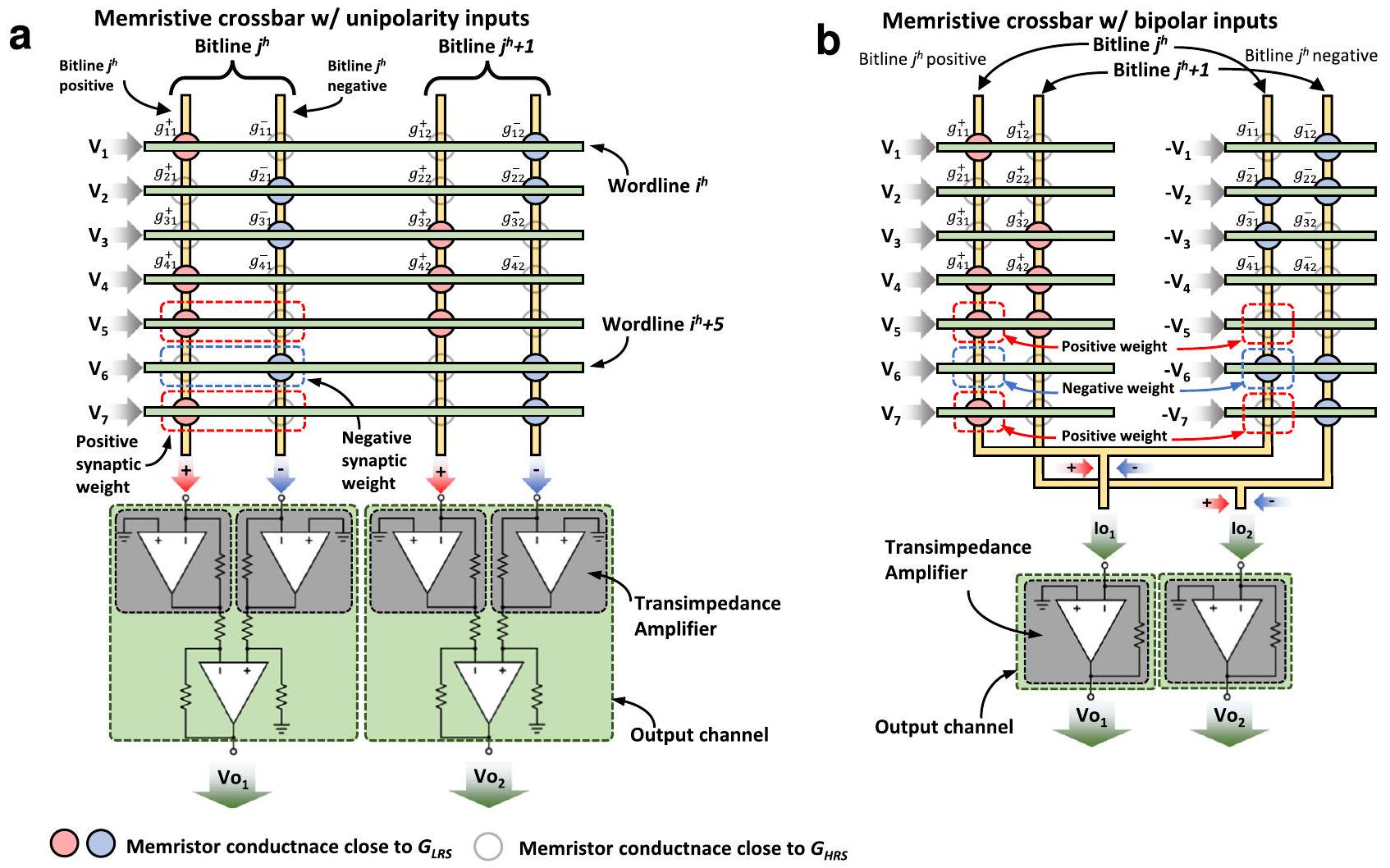
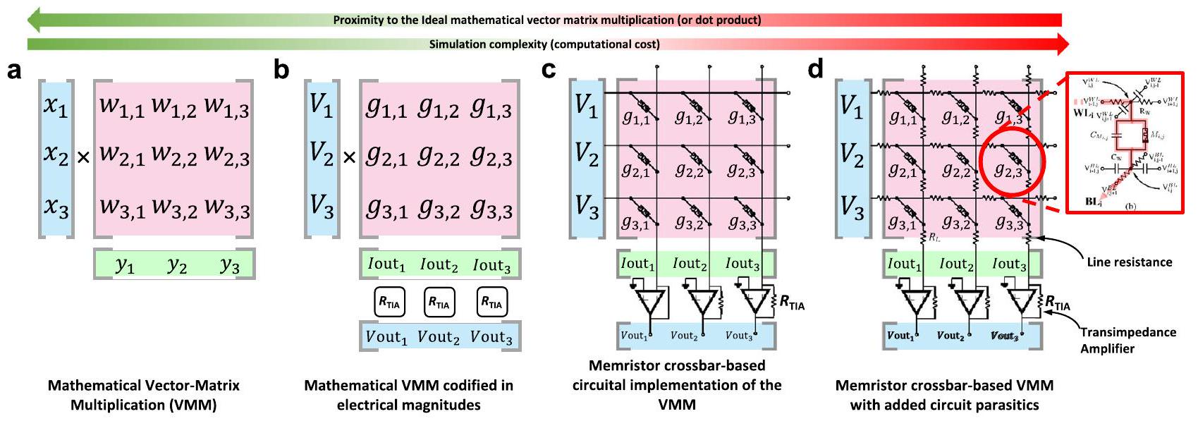
ميمريستور (1 R أو 1 M) أو مصفوفة تشابكية سلبية (الشكل 3c). عند استخدام مصفوفات تشابكية من الميمريستورات لأداء عمليات VMM، قد تكون هناك حاجة إلى دوائر إضافية عند الإدخال والإخراج لاستشعار و/أو تحويل الإشارات الكهربائية (انظر الصناديق الحمراء في الشكل 2). من أمثلة هذه الدوائر محولات من الرقمية إلى التناظرية (DAC)، ومن التناظرية إلى الرقمية (ADC) ومضخمات مقاومة التيار (TIA). لاحظ أن دراسات أخرى استخدمت تنفيذات تختلف قليلاً عن هذا المخطط، أي، دمج أو تجنب كتل معينة لتوفير المساحة و/أو تقليل استهلاك الطاقة (انظر الجدول 1).
في الأقسام الفرعية التالية، نصف بالتفصيل جميع الكتل الدائرية المطلوبة لتنفيذ كامل للأجهزة لشبكة عصبية ميمريستيف. لتوفير صورة عالمية واضحة وشرح تفصيلي، تتوافق عناوين الأقسام الفرعية مع أسماء الكتل في الشكل 2.

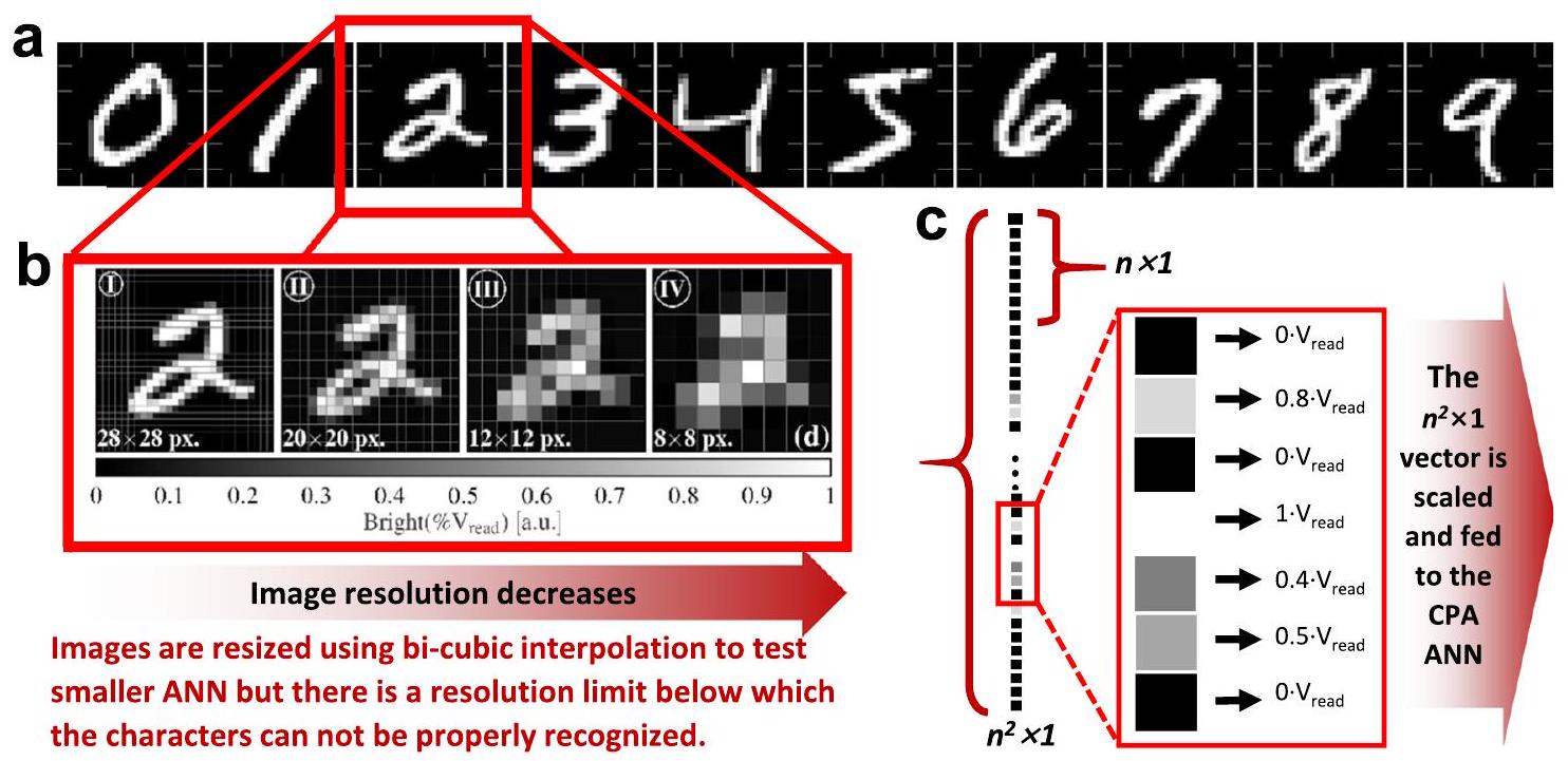
أجهزة التقاط الصور (الكتلة 1) وتشكيل متجه الإدخال (الكتلة 3)

الصورة (أو النمط) هي مجموعة من البكسلات بألوان مختلفة مرتبة في شكل مصفوفة (يشار إليها باسم في هذه المقالة). في هذا العمل، سنعتبر الصور بالأبيض والأسود، حيث يمكن تشفير لون تلك البكسلات بقيمة واحدة فقط. ومع ذلك، في الصور الملونة، يتم تمثيل كل بكسل بـ 3 (في ترميز RGB) أو 4 (في ترميز CMYK) قيم، مرتبة بطريقة تنسورية، أي، أو . يتم إجراء كل من التدريب والاختبار لشبكة عصبية لتصنيف الصور من خلال تقديم مجموعات بيانات كبيرة من الصور إلى مدخلاتها. في شبكة عصبية حقيقية، يمكن أن تأتي كل صورة مباشرة من كاميرا مدمجة (الكتلة 1)، أو يمكن تقديمها كملف من قبل المستخدم (الكتلة 2). اعتمادًا على تنسيق الصورة (على سبيل المثال، أبيض/أسود، 8 بت *.bmp، 24 بت *.bmp، *.jpg، *.png، من بين العديد من الآخرين) سيكون نطاق الألوان الممكنة (المشفرة كقيم عددية) لكل بكسل مختلفًا. كل من الطرق المذكورة أعلاه لتغذية الصور إلى الشبكة العصبية تعني أعباء أجهزة مختلفة. في حالة تصنيف الصور أثناء الطيران، من الضروري وجود جهاز تصوير CMOS لالتقاط الصور المدخلة . على سبيل المثال، المرجع 84 يستخدم مستشعر صورة بكسل ، حيث يتكون كل بكسل من ثنائي ضوئي وأربعة ترانزستورات تولد إشارة تناظرية تكون سعتها متناسبة مع شدة الضوء. ثم يتم إنشاء صورة ثنائية بكسل عن طريق رسم بكسلات الجوار في بكسل واحد في الصورة الثنائية. يتم اعتبار نهج مشابه في المرجع 85 حيث يتم التقاط صورة بكسل بواسطة مستشعر الصورة ثم يتم تغيير حجمها إلى صورة . سيتم تغطية إجراء تغيير الحجم وضرورة مثل هذا الإجراء لاحقًا في هذا القسم الفرعي.
الشكل 3 | نوى ضرب المصفوفات غير فون نيومان (VMM) المبلغ عنها في الأدبيات. أ مصفوفة تشابكية SRAM (ذاكرة الوصول العشوائي الثابتة) كاملة CMOS، مصفوفة تشابكية هجينة من الميمريستور/CMOS 1T1R و مصفوفة تشابكية سلبية كاملة من الميمريستور. تفترض جميع الحالات هيكل تكامل مصفوفة تشابكية تقوم بأداء عملية الضرب والتراكم (MAC) من خلال استغلال قانون كيرشوف للتيارات. يسمح استخدام الميمريستورات بمساحة أصغر لكل تشابك حيث يتم استخدام عدد أقل من الأجهزة الأصغر. تسمح مصفوفات التشابك السلبية من الميمريستورات بأعلى كثافة تكامل ممكنة، ومع ذلك، لا تزال تقنية غير ناضجة
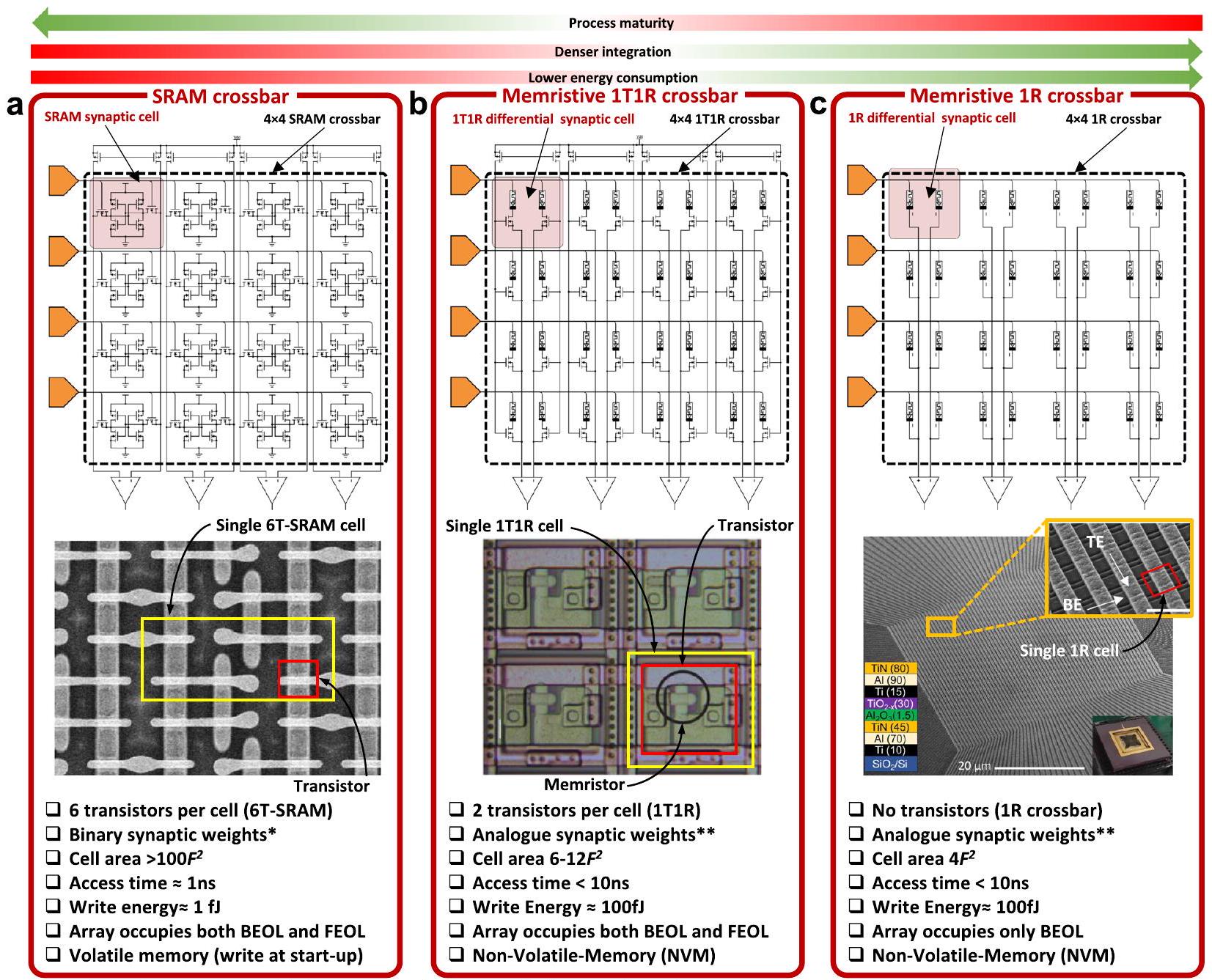
  • يمكن أن يكون التخزين متعدد المستويات ممكنًا بواسطة خلايا SRAM أكثر تعقيدًا (مساحة خلية أكبر)
    ** الوزن التشابكي التناظري مرغوب فيه ولكن عادةً ما يتوفر عدد محدود فقط من المستويات المستقرة
    مع الكثير من المجال للتحسين. ياماكا، م. SRAM منخفض الطاقة. في: كاواهارا، ت.، ميزونو، هـ. (محررون) الحوسبة الخضراء مع الذاكرة الناشئة. سبرينغر، نيويورك، نيويورك (2013)، معاد إنتاجه بإذن من SNCSC. تم تعديله بإذن بموجب ترخيص CC BY 4.0 من المرجع 54. تم تعديله بإذن بموجب ترخيص CC BY 4.0 من المرجع هو حجم الميزة للطباعة وتقدير الطاقة على مستوى الخلية. FEOL و BEOL تعني مقدمة خط الإنتاج ونهاية خط الإنتاج، على التوالي.
    القسم. تعتبر كلتا الحالتين FPGA من أجل واجهة نظام اكتساب الصورة (أي مستشعر الصورة CMOS وخوارزمية تغيير الحجم) مع مصفوفة الميمريستور ودائرتها المحيطية. من ناحية أخرى، ركزت بعض الدراسات بشكل حصري على استخدام مصفوفة الميمريستور على واجهة اتصال على الشريحة للحصول على الصورة من جهاز كمبيوتر (على سبيل المثال، المرجع 54 يستخدم منفذ اتصال تسلسلي) تم تشكيله بالفعل في تنسيق الإدخال المطلوب.
فيما يتعلق بالصور المدخلة، هناك مجموعات بيانات متعددة من الصور متاحة عبر الإنترنت لتدريب واختبار الشبكات العصبية. بعض من أكثرها استخدامًا هي: 1) MNIST (المعهد الوطني للمعايير والتكنولوجيا المعدل)، والذي هو في الأساس مجموعة بيانات تحتوي على 70,000 صورة بالأبيض والأسود تظهر أرقام مكتوبة بخط اليد من 0 إلى 9 (أي، حوالي 7,000 لكل رقم)؛ 60,000 منها تستخدم للتدريب و 10,000 للاختبار ؛ 2) CIFAR (المعهد الكندي للبحث المتقدم)، الذي يحتوي على 60,000 صورة ملونة مقسمة إلى 10 فئات لـ CIFAR-10 و 100 فئة لـ CIFAR-100 ؛ 3) ImageNet، واحدة من أكبر مجموعات بيانات الصور، والتي تتكون من أكثر من 1.2 مليون صورة مصنفة من 1000 فئة لمسابقة ImageNet . تعتبر MNIST نقطة انطلاق جيدة
نظرًا لأن هذه المجموعة البسيطة يمكن تصنيفها حتى مع الشبكات العصبية الصغيرة. لتقييم جهاز أو شريحة، من الضروري تقييم دقة نماذج الشبكات العصبية العميقة القياسية مثل و ResNet على مجموعة بيانات CIFAR و ImageNet من خلال استخدام محاكاة على مستوى الهيكل وإحصائيات الأجهزة الواقعية . للتوضيح، هنا نوضح مع مجموعة بيانات MNIST. عدد الأنواع/الفئات من الصور (يشار إليها باسم في هذه المقالة) في مجموعة بيانات MNIST هو 10. يتم ضغط الصور في .idx3-ubyte ملف يمكن فتحه باستخدام MATLAB؛ كل منها يأتي بتدرج الرمادي وبدقة بكسل. في بايثون، يمكن العثور على صور MNIST مضمنة في مكتبة تُدعى Keras. تُستخدم صور التدريب لتمكين الشبكة العصبية الاصطناعية من فهم الميزات المميزة لكل نمط (أي الأرقام)، وتُعرض صور الاختبار على الشبكة العصبية الاصطناعية (بعد التدريب) لتصنيفها. يمكن رؤية بعض الأمثلة على هذه الصور في الشكل 4a، حيث X و المحور يمثل مؤشر البكسل. يتم ترميز سطوع البكسل في 256 مستوى رمادي بين 0 (مطفأ بالكامل، أسود) و255 (مضاء بالكامل، أبيض). في مجموعة بيانات MNIST، كل من 60,000 تُعبر صور التدريب عن متجه عمودي، وجميع هذه المتجهات أفقياً
الجدول 1 | قائمة بالنماذج الأولية المبلغ عنها في الأدبيات وتفاصيل كيفية تنفيذ كل كتلة (برمجيات/أجهزة خارج الشريحة/أجهزة داخل الشريحة، إلخ)
عمل(ات) جهاز نوع الشبكة العصبية / مجموعة البيانات حجم العارضة عقدة CMOS ADC تركيب الخلية دائرة الإدخال (DAC) إلكترونيات الاستشعار دالة التنشيط محددات الصف/العمود دالة تفعيل سوفت ماكس الاستدلال/ التدريب دائرة وزن البرنامج
57 SLP، الترميز النادر، MLP/ الحروف اليونانية 180 نانومتر على الشريحة (13-بت) على الشريحة (6 بت) تكامل الشحنة رقمي على الشريحة (سيغمويد) على الشريحة خارج الشريحة (البرمجيات) الاستدلال والتدريب على الشريحة
٥٥ TiN/TaOx/ HfOx /TiN سي إن إن / MNIST 130 نانومتر خارج الشريحة (8 بت) تي تي 1 آر على الشريحة (1-بت) تكامل الشحنة خارج الشريحة (البرمجيات: ReLU والتجمع الأقصى) على الشريحة خارج الشريحة (البرمجيات) الاستدلال والتدريب خارج الشريحة
١٠٢ Pt/Ta/Ta2O5/ Pt/Ti MLP/MNIST غير متوفر تي تي 1 آر غير متوفر غير متوفر عتاد خارجي: ReLU خارج الشريحة خارج الشريحة (البرمجيات) التعلم والتدريب خارج الشريحة
61 لا توجد بيانات (تطوير ملكي) بي إن إن، MNIST، CIFAR-10 90 نانومتر على الشريحة (3 بت) 1T1R لم يتم التنفيذ على الرقاقة (VSA) على الشريحة (ثنائي) على الشريحة خارج الشريحة (البرمجيات)* استنتاج فقط خارج الشريحة
113 تا/تا أوكس/بلاتين سي إن إن / MNIST 180 نانومتر على الشريحة تي تي 1 آر على الشريحة على الشريحة (TIA) خارج الشريحة (البرمجيات)* على الشريحة خارج الشريحة (البرمجيات)* استنتاج فقط خارج الشريحة
١١٤، ١١٥ تاوكس سي إن إن/ MNIST 180 نانومتر على الشريحة (10 بت) تي تي 1 آر على الشريحة على الرقاقة (TIA) خارج الشريحة (البرمجيات)* على الشريحة خارج الشريحة (البرمجيات)* استنتاج فقط خارج الشريحة
٢١٩ W/TiN/TiON بي إن إن/ MNIST 65 نانومتر على الشريحة (3 بت) 1T1R غير متوفر على الرقاقة (CSA) خارج الشريحة (FPGA: أقصى تجميع) على الشريحة خارج الشريحة (FPGA) استنتاج فقط خارج الشريحة
١١٦ تا/ Pd/ HfO2/ Pt/ Ti سي إن إن/ ‘ U ‘، ‘ M ‘، ‘, ‘ لا توجد بيانات خارج الشريحة 1T1R على الشريحة خارج الشريحة (TIA) على الشريحة (ReLU)، خارج الشريحة (البرمجيات: التجميع الأقصى) خارج الشريحة خارج الشريحة (وحدة التحكم الدقيقة) الاستدلال والتدريب خارج الشريحة
272 TiN/HfO2/Ti/TiN بي إن إن / MNIST، CIFAR-10 1 كيلوبايت 130 نانومتر على الشريحة 2T2R لم يتم التنفيذ أونشيب (PCSA) على الشريحة (ثنائي) على الشريحة على الشريحة (ثنائي) استنتاج فقط خارج الشريحة
99 MLP/MNIST 2 ميغابايت 180 نانومتر على الشريحة (1-بت) 1T1R على الشريحة (1-بت) على الشريحة لا توجد بيانات على الشريحة لا توجد بيانات استنتاج فقط خارج الشريحة
100 ألCu/TiN/Ti/ MLP/ 150 نانومتر على الشريحة (1 أو 3 بت) 1T1R على الشريحة (1-بت) على الشريحة خارج الشريحة (البرمجيات)* على الشريحة خارج الشريحة (البرمجيات)* استنتاج فقط ذاكرة الوصول العشوائي الساكنة على الشريحة (SRAM)
١٢٢ PCM (لا توجد بيانات أخرى) MLP/MNIST 180 نانومتر لا توجد بيانات 3T1C + 2PCM لا توجد بيانات خارج الشريحة (البرمجيات) خارج الشريحة (البرمجيات: ReLU) خارج الشريحة خارج الشريحة (البرمجيات) استنتاج فقط خارج الشريحة
71,73 PCM (لا توجد بيانات أخرى) MLP/MNIST، ResNET-9/ CIFAR-10 14 نانومتر على الشريحة 4T4R على الشريحة (8 بت) على الرقاقة (مبني على CCO) على الشريحة (ReLU) على الشريحة خارج الشريحة (البرمجيات) استنتاج فقط على الشريحة
72 PCM (لا توجد بيانات أخرى) MLP/MNIST 14 نانومتر خارج الشريحة 4T4R على الشريحة (8 بت) على الشريحة خارج الشريحة (سيغمويد) على الشريحة خارج الشريحة (FPGA) استنتاج فقط على الشريحة
273 لا توجد بيانات سي إن إن / CIFAR-10 55 نانومتر على الشريحة تي تي 1 آر لا توجد بيانات على الشريحة خارج الشريحة (FPGA) على الشريحة خارج الشريحة (FPGA) استنتاج فقط خارج الشريحة
٢٧٤ TiN/HfO2/Ti/TiN سي إن إن/ MNIST 18 كيلوبايت 130 نانومتر خارج الشريحة* تي تي 1 آر خارج الشريحة* خارج الشريحة* خارج الشريحة (FPGA) خارج الشريحة* خارج الشريحة (FPGA) استنتاج فقط على الشريحة
123 TiN/HfO2/Ti/TiN بي إن إن/ MNIST 1 كيلوبايت 130 نانومتر غير متوفر 2T2R غير متوفر على الشريحة خارج الشريحة (البرمجيات)* على الشريحة خارج الشريحة (البرمجيات)* استنتاج فقط خارج الشريحة
٢٧٥ MLP/MNIST 158.8 كيلوبايت 130 نانومتر على الشريحة (8 بت) 2T2R على الشريحة (8 بت) تكامل الشحنة خارج الشريحة على الشريحة خارج الشريحة استنتاج فقط خارج الشريحة (FPGA)
60 تاو/تين سي إن إن / MNIST، CIFAR-10 130 نانومتر على الشريحة (8 بت) 1T1R على الشريحة تكامل الشحنة على الشريحة (تناظري: ReLU)، خارج الشريحة (FPGA: تجميع أقصى) على الشريحة خارج الشريحة (FPGA) خارج الشريحة (البرمجيات) على الشريحة
الشكل 4 | مثال على قاعدة بيانات صور شائعة الاستخدام لتدريب واختبار الشبكات العصبية الاصطناعية، وكيف يتم إدخالها إلى الشبكة. أ عينات من مجموعة بيانات MNIST للأرقام المكتوبة بخط اليد التي تم اعتبارها في هذه المقالة. في جميع الحالات، يتم تمثيل الصور في سطوع البكسل (أو الشدة) مُرمز في 256 مستوى يتراوح من 0 (مطفأ بالكامل، أسود) إلى 1 (مضاء بالكامل، أبيض). ب فقدان القابلية للقراءة كـ
تنخفض الدقة من بكسلات (الحالة I) إلى (الحالة الرابعة). ج تمثيل تخطيطي لفك لف بكسلات الصورة. لاحظ أن كل من تُجمع أعمدة الصور من وحدات البكسل عموديًا للوصول إلى متجه عمودي. ثم يتم توسيعه بواسطة لإنتاج متجه من الفولتية التناظرية التي يتم تغذيتها إلى الشبكة العصبية الاصطناعية.
مُتَسَلسِلَة لعرض مصفوفة. وبالمثل، تتكون مجموعة بيانات الاختبار من المصفوفة. في كلتا الحالتين، كل من يجب تغذية البيكسلات إلى مصفوفة التقاطع لمزيد من المعالجة.
كما ذُكر سابقًا، يجب أن تحتوي أبسط هياكل الشبكات العصبية الاصطناعية (البرسيبترونات متعددة الطبقات) على عدد من المدخلات يساوي عدد البيكسلات الموجودة في الصور المراد تصنيفها. في الشبكات العصبية الاصطناعية المعتمدة على البرمجيات، لا تمثل هذه مشكلة. ومع ذلك، فإن المدخلات المتاحة في الشبكات العصبية الاصطناعية المعتمدة على الأجهزة محدودة بحجم مصفوفة الميمريستور الأقصى. في الأدبيات، تم التعامل مع مثل هذا التحدي من خلال اعتبار نهج مختلفة: على سبيل المثال، بالنظر إلى مجموعة بيانات MNIST التي تحتوي على صور بدقة بكسلات، إحدى الخيارات هي تنفيذ الطبقة المشبكية باستخدام عدة تقاطعات لتناسب 784 مدخلاً (على سبيل المثال، أو ستكون هناك حاجة إلى القضبان العرضية ومع ذلك، بالنسبة للجهود البحثية التي تركز على مستوى الجهاز، فإن هذا عادة ما يكون خارج نطاق الوصول لأنه يتطلب دمجًا غير مباشر بين CMOS والميمريستور. خيار آخر هو النظر في الشبكات العصبية الأكثر تعقيدًا، مثل الشبكات العصبية التلافيفية (CNN). الطبقة الأولى من LeNet-5 (نوع من الشبكات العصبية التلافيفية) هي التي يمكن تنفيذها مع العارضة. في الواقع، تعتمد مهام تصنيف الصور في التعلم العميق الحديث عادةً على طبقة تلافيفية. أما بالنسبة للحالة السابقة، فإن تنفيذ ذلك ليس سهلاً لمشاريع البحث التي تركز على مستوى الجهاز، حيث يتطلب أيضًا تكاملًا معقدًا بين CMOS والميمريستور. ومع ذلك، في بعض الحالات، يتم تنفيذ أولى الطبقات التلافيفية على البرمجيات وخارج الشريحة لتقليل أبعاد الصورة، ثم يتم تغذية المتجه الناتج إلى الجزء الميمريستيف من الشبكة العصبية الاصطناعية. لاحظ أنه في هذه الحالة، لا يتم تمثيل عدم مثالية الأجهزة بشكل متساوٍ في جميع أنحاء الشبكة، ويتم تقييم تأثيرها فقط على الجزء المتصل بالكامل. . أخيرًا، الخيار الآخر هو إعادة قياس كل من الصور في مجموعة بيانات MNIST الأصلية (في هذا العمل، ممثلة بالكتلة 3). على سبيل المثال، إذا كان لدينا 64 مدخلًا في الشريط المتقاطع، فسيكون من الضروري إعادة قياس الصورة من إلى (أي 64 بكسل)؛ سيتم الإشارة إلى حجم الصورة المعاد تحجيمها بـ يمكن إجراء إعادة القياس بسهولة عبر البرمجيات، باستخدام على سبيل المثال MATLAB ومجموعة أدوات التعلم العميق الخاصة به كلغة/منصة لتنفيذ هذا النوع من العمليات الحسابية، أو Python مع مكتبات TensorFlow وKeras أو Pytorch. ومع ذلك، كما هو موضح في الشكل 4b، تصبح الصور المعاد قياسها بشكل مفرط بالكاد قابلة للقراءة وبالتالي يتغير مجموعة البيانات بالكامل وكذلك المعيار، أي نتائج الاستدلال التي تم الحصول عليها لـ يجب مقارنة الصور المعاد قياسها من MNIST فقط
مع نتائج MNIST وليست مع نتائج معيار MNIST الأصلية. هذا مشابه لاستخدام مجموعة بيانات مصنوعة خصيصًا. مع وضع ذلك في الاعتبار، ونظرًا للاستخدام المتكرر لهذه المنهجية في الأدبيات، سنأخذ في الاعتبار استخدامها مع التأكيد على الاعتبارات المذكورة أعلاه، ونشجع المؤلفين على عدم إعادة قياس مجموعة بيانات الصور إذا كانوا يهدفون إلى مقارنة نتائجهم مع مجموعات البيانات الأصلية.
كمثال، يوضح الخوارزم الإضافي 1 كود MATLAB المستخدم لإعادة تحجيم مجموعة بيانات الصور من إلى بكسل. قبل تقليل حجم الصور، يجب إعادة تشكيل كل منها من متجه عمودي إلى مصفوفة، باستخدام دالة MATLAB reshape(). ثم، يتم تغيير حجم الصورة إلى الحجم المطلوب الحجم بالبكسل بواسطة دالة MATLAB imresize() . هذه الوظيفة تستقبل كوسيلة للمعالجة طريقة تقليل العينة المرغوبة، والتي تم اختيارها في هذا المثال لتكون الاستيفاء الثنائي المكعب (كما في مقالات أخرى في مجال الميمريستيف) ). تظهر نتائج إعادة القياس لصورة واحدة في الشكل 4ب. لاحظ أنه باستخدام هذه الطريقة، من المتوقع أن تكون القيم خارج نطاق [ 0,1 ]. وبالتالي، يتم معالجة الصورة المنقوصة وأي قيمة ناتجة تتجاوز هذا النطاق يتم تقليمها إلى 0 أو 1 . ثم يتم إعادة تشكيل الصور المعاد قياسها إلى تنسيق تمثيل متجه العمود وتخزينه في مصفوفة جديدة. الآن يمكن استخدام هذه الصورة كمدخل في مصفوفة التوصيل لميمريستور.

دوائر القيادة المدخلة (الكتلة 4)

لون كل بكسل في الصورة (يمثل كـ العمود) يتم ترميزه كجهد يُطبق على صف في الشبكة المتقاطعة (أي، خط الكلمة)، كما هو موضح في الشكل 4c، مما يؤدي إلى متجه الجهود التناظرية . إذا كانت الصورة بالأبيض والأسود (أي، قيمتان ممكنتان)، فإن قيم الجهد كل بكسل سيكون 0 و ( كونه جهد مرجعي محدد بواسطة التطبيق)؛ ومع ذلك، يمكن أن يتراوح لون كل بكسل أيضًا ضمن تدرج الرمادي، مما يؤدي إلى مجموعة من الجهود التناظرية. على سبيل المثال، لون كل بكسل في 8 بت صور مجموعة بيانات MNIST (وبالتالي، لون كل بكسل في الصورة المعاد حجمها الصورة المدخلة إلى المبدل) تتراوح ضمن تدرج رمادي من 256 قيمة ممكنة (مشفرة في التمثيل الثنائي من 00000000 إلى 11111111)، مما يعني أن الفولتية التي يجب تطبيقها على كل مدخل من مداخل الشبكة المتقاطعة يمكن أن تأخذ قيمًا مثل إلخ حتى . لذلك، من الضروري وجود محول رقمي إلى تناظري (DAC) بعمق 8 بت لكل مدخل لتحويل الشيفرة المكونة من 8 بتات إلى جهد واحد. عندما يتم استخدام الشبكة العصبية الاصطناعية (ANN) للتعرف على أنواع أخرى من
الشكل 5 | مخططات تخطيطية لدارات DAC المستخدمة تقليديًا في الأدبيات لتحفيز صفوف الشبكة المتقاطعة للذاكرة. أ دالة ثنائية ذات وزن N بت. محول التيار الحالي محول رقمي تماثلي ذاكرة محول رقمي إلى تناظري R-2R بعمق N بت محول رقمي إلى تناظري (DAC) يعتمد على تعديل عرض النبضة (PWM).
تتطلب الصور المشفرة بتنسيق مختلف (مثل 24 بت) محولات رقمية تماثلية (DACs) بدقة مختلفة. يعتمد التنسيق الذي تُعرض به الصور على التطبيق النهائي للشبكة، أي أن الشبكات العصبية الاصطناعية (ANNs) لتحديد أرقام اللوحات قد تعمل بشكل جيد مع الصور بالأبيض والأسود (أي 1 بت)، بينما قد تحتاج الشبكات العصبية الاصطناعية لتحديد الأجسام إلى النظر في 24 بت (16.7 مليون) لون. تُعرض أمثلة على محولات DAC المستخدمة غالبًا في الشبكات العصبية الاصطناعية الميمريستيفية في الشكل 5: DAC ثنائي الوزن N-بت (الشكل 5a)، DAC بتوجيه التيار (الشكل 5b)، DAC ميمريستيفي (الشكل 5c)، DAC R-2R N-بت (الشكل 5d) وDAC القائم على تعديل عرض النبضة (PWM) (الشكل 5e).
تحديد دقة محولات الرقمية إلى التناظرية (DACs) عند مدخل كل صف من صفوف الشبكة المتقاطعة هو عامل حاسم يؤثر على استهلاك الطاقة، والمساحة، ومقاومة الخرج لشبكة الأعصاب الاصطناعية – حيث أن تقليل المقاومة مهم لتحقيق شبكات متقاطعة كبيرة. تتكون محولات DAC التقليدية عالية الدقة ذات المقاومة المنخفضة من نواة DAC مع مضخم عمليات (في تكوين عازل) كمرحلة خرج من أجل تقليل مقاومة الخرج. وبالتالي، يمكن تقسيم فقدان الطاقة في DAC إلى الطاقة الناتجة عن التبديل/التسرب لنواة DAC الرقمية والطاقة الثابتة/الديناميكية لمضخم العمليات. من ناحية، يمكن تقدير فقدان الطاقة في نواة DAC الرقمية على أنه ، حيث هو تردد الإخراج، هو الطفيلي
السعة هو جهد الإمداد، و هو طاقة التسرب التي تعتمد على عقدة التكنولوجيا، ولتكنولوجيا 65 نانومتر مع مصدر طاقة 1 فولت تكون في حدود عدة بيكو واط في العاكس. من ناحية أخرى، يمكن تقدير فقدان الطاقة في الكتلة التناظرية من خلال افتراض مرحلة متابع من الفئة AB، مع كفاءة في هذا السيناريو، تساوي القدرة الثابتة لهذه الوحدة قدرتها الديناميكية ويمكن حساب مجموعهما كـ ، حيث هو عدد الميمريستورز التي يجب تشغيلها و هو الحد الأدنى لمقاومتهم. تحت ترددات تقارب هو السائد، بينما فوق هذا العتبة، فإن الطاقة المبددة أثناء التبديل تجعل أكبر من .
بالنسبة لمساحة السيليكون المطلوبة لمحوّلات الرقمية إلى تماثلية (DACs)، فإنها تُحدد بشكل رئيسي بواسطة دقة DAC، والتي تحددها بدورها مطابقة عناصر الضوضاء في الجهاز. بالنسبة لمحوّلات DAC التي تعتمد على المقاومات، فإن المصدر الرئيسي للضوضاء يأتي من مضخم العمليات CMOS في مرحلة الخرج. يمكن تقليلها باستخدام ترانزستورات أكبر (من حيث العرض والطول) لزوج الإدخال التفاضلي. وبالمثل، لتعظيم التوافق بين المقاومات المرجعية، يُشجع على استخدام أجهزة أوسع، مما يساهم في زيادة المساحة السيليكونية المطلوبة لكل محول رقمي إلى تماثلي (DAC).
لتقليل مساحة السيليكون واستهلاك الطاقة، كلما كانت دقة المحول الرقمي إلى التناظري (DAC) أقل كان ذلك أفضل. ونتيجة لذلك، بالإضافة إلى الترميز القائم على السعة لمدخلات الشبكة المتقاطعة، يتم أيضًا النظر في مخططات الترميز الزمني. على سبيل المثال، في أنظمة تعديل عرض النبضة (PWM)، يتم ترميز المدخلات بأطوال نبضات مختلفة. 256 ثانية، إلخ حتى ). هذا يسمح بتجاوز عدم خطية الجهاز ولكنه يعاني من انخفاض في معدل النقل . بدلاً من ذلك، في ما يُعرف بالتشفير التسلسلي للبتات تُقدم المدخلات عالية الدقة عبر الشبكة على شكل تيار من نبضات الجهد ذات السعة والعرض الثابتين على سبيل المثال، لتمثيل مدخلات الكروس بار بعمق 16 بت، تُرسل إشارات الجهد ذات الـ -bit إلى صف الكروس بار عبر دورات الزمن . بعد حساب VMM، يتم تجميع المنتجات الجزئية (مخرجات كل خطوة زمنية) معًا لتشكيل قيمة الإخراج النهائية. أيضًا، العديد من الأوراق لقد استكشفت حالة الشبكات العصبية الاصطناعية مع المدخلات الثنائية، حيث تستخدم أبسط محولات رقمية تماثلية (1-بت). في حالة تدفق المدخلات 1-بت، يمكن أيضًا استبدال المحولات الرقمية التماثلية بمبدلات متبوعة بمضخم إخراج للسماح للمبدل بتشغيل جميع الأجهزة المتصلة بـ . بالإضافة إلى ذلك، فإن الحساب باستخدام المدخلات المشفرة زمنياً يتأثر بشكل أقل بتغيرات الضوضاء، التي تؤثر في الغالب على سعة إشارات المدخلات بدلاً من عرض النبضة. ومع ذلك، فإن العيب في أنظمة التشفير الزمني هو تقليل سرعة الحساب والعبء المادي المطلوب لحساب المجموعات الجزئية. .
بديل للحفاظ على معدل نقل مرتفع واستخدام محول رقمي تماثلي منخفض الدقة هو استخدام الحوسبة التقريبية. عند استخدام محولات الرقمية إلى التناظرية ذات الدقة المنخفضة (1- أو 2- أو 3-بت)، هناك فرصة أكبر لوجود مدخلات متعددة تتطلب نفس جهد القيادة، مما يسمح بمشاركة المحولات بين عدة خطوط، وبالتالي توفير الطاقة والمساحة. ومع ذلك، يجب أن يؤخذ في الاعتبار أن مقاومة الخرج للمحول تحد من عدد خطوط الكلمات التي يمكن تحييدها. أيضًا، تتطلب هذه الطريقة استخدام مضاعفات تناظرية (الكتلة 11) بين دوائر القيادة المدخلة وعبور الميمريستور، مما يؤدي إلى زيادة الحمل على دوائر التحكم. تكمن المشكلة في استخدام محولات ذات دقة منخفضة عند مدخل العبور في فقدان دقة عملية VMM. وبالتالي، هناك توازن جوهري بين جميع هذه المتغيرات. يمكن أيضًا تقليل فقدان الدقة من خلال استغلال تقنيات التدريب المعتمدة على البرمجيات للشبكات العصبية الكمية.

نواة VMM (الكتلة 5)

الجهود الناتجة عن كل محول رقمي إلى تناظري (DAC) (التي تمثل لون كل بكسل من الصورة المعاد قياسها تُطبق (الصورة) عند المدخلات (الصفوف) من مصفوفة القضبان المتقاطعة من الميمريستورز. تصف موصلية كل ميمريستور داخل القضبان المتقاطعة الاتصال المشبكي بين كل خلية عصبية مدخلة (i) وكل خلية عصبية مخرجة (j). يتم استخدام هذا المخطط في أوراق بحثية متنوعة. . ومع ذلك، يعتبر البعض أيضًا أن هناك مصطلح انحياز مضاف إلى المجموع الموزون المدخل إلى الخلية العصبية . يمكن القيام بذلك رقميًا وخارجيًا، أو في المجال التناظري. إذا تم القيام بذلك بطريقة تناظرية، فستكون هناك حاجة إلى صف إضافي في الشبكة المتقاطعة، مما يتطلب شبكة متقاطعة من . هذه العملية تنتج متجه صف بحجم (انظر المعادلة 1). في نظام الحوسبة التقليدي من نوع فون نيومان، يتم تنفيذ VMM من خلال القيام بكل عملية فرعية (الضربات والجمع) بشكل متسلسل، مما يستغرق وقتًا طويلاً؛ علاوة على ذلك، يزداد وقت الحساب بشكل تربيعي مع زيادة أبعاد مصفوفات الإدخال. ، أو في حالة استخدام ما يُسمى بتدوين Big-O، فإن خوارزمية VMM لها تعقيد زمني قدره . تسمح تقاطعات الميمريستور (مثل تلك الموضحة في الشكل 6a) بإجراء عمليات VMM بسهولة وسرعة أكبر لأن جميع العمليات الفرعية تتم بشكل متوازي. في التقاطع، يتم ترميز سطوع (لون) كل بكسل في كل صورة من حيث الفولتية التناظرية وتطبيقها على الصفوف المدخلة (المعروفة أيضًا بخطوط الكلمات والمتصلة بأقطاب الميمريستور العلوية)، بينما يتم تأريض الأعمدة الناتجة (المعروفة أيضًا بخطوط البت والمتصلة بأقطاب الميمريستور السفلية) من خلال مضخم مقاومة الترانسيميدانس (انظر الشكل 6b لتمثيل مثالي). ثم يتم إجراء VMM بطريقة تناظرية، حيث يتم تحديد التيار المتدفق عبر كل ميمريستور بواسطة الفولتية المطبقة على الخط والمقاومة لـ
كل ميمريستور ( ). لاحظ أنه في زوج يمثل صف التقاطع، و j يمثل عمود التقاطع. ثم يتم جمع التيارات المتدفقة عبر الميمريستورات المتصلة بخط بت معين واستشعارها لتشكيل متجه الناتج. دعنا نعتبر التدوين التالي لشرح هذه الفكرة بشكل أفضل:
لتصنيف صور MNIST بدقة بكسل مع ANN، تتطلب عمليات VMM متعددة، حيث يتم تعريف مصفوفة المقاومات في المعادلة 1 بناءً على مصفوفة من الأوزان المشبكية، التي لها حجم ، وجميع الأرقام التي تشكلها هي أرقام حقيقية ( ) مع إمكانية وجود قيم إيجابية وسلبية – الطريقة التي يتم بها حساب موصوفة بالتفصيل في قسم تدريب ANN وتحديث الوزن المشبكي (الكتل 2، 11-15): خوارزمية التعلم. نظرًا لأن القيم السلبية لا يمكن تمثيلها مباشرة باستخدام الميمريستورات، تم اعتماد بعض الاستراتيجيات. أضاف المرجع 104 عمودًا إضافيًا في التقاطع (يسمى عمود المرجع، انظر السهم الأزرق في الشكل 6c) مع جميع ميمريستوراتها مضبوطة على ، ليصبح المجموع ميمريستورات في التقاطع. ثم يتم الحصول على التيار الكلي عند مخرج التقاطع عن طريق طرح التيار الناتج عن عمود المرجع {ref} من التيار الناتج عن عمود (انظر الشكل 6c). يتم تمثيل هذا المفهوم رياضيًا في المعادلة 2.
حيث يمثل المقاومات لعمود المرجع و يتم حسابه بطريقة تجعل الأجهزة ذات المقاومة فوق تنتج أوزان مشبكية إيجابية، وتلك التي لديها مقاومة أقل من تنتج أوزان مشبكية سلبية . لهذه الاستراتيجية عيبان: من ناحية، يمكن للمرء استخدام نصف الحالات المعروضة من قبل الميمريستور للأوزان الإيجابية والنصف الآخر للأوزان السلبية، مما يقلل من النطاق بين الوزن الأقصى والأدنى. من ناحية أخرى، فإن توجيه عمود المرجع إلى بقية أعمدة التقاطع لإجراء عملية الطرح المقابلة ليس بالأمر السهل. استراتيجية أخرى هي استخدام ميمريستورين لكل وزن مشبكي، مما يؤدي إلى وجود تقاطعين من . ضمن هذا النهج، يمكن إعادة كتابة المعادلة 2 كـ
حيث يتم ترميز المقاومات الإيجابية والسلبية بواسطة زوج من الميمريستورات المجاورة ( و )، كل منهما مضبوط على قيمة إيجابية من المقاومة. تم اختيار هذه الطريقة التمثيلية، الموضحة في الشكل 6d، في هذه الدراسة لأنها تضاعف نطاق

مستويات المقاومة في التقاطع، مما يجعلها أقل عرضة للضوضاء والتغيرات .
لحساب قيمة المقاومة المطلوبة لكل من الميمريستورات في الزوج، نبدأ بتقسيم إلى مصفوفتين و كالتالي:
كل منهما يحتوي فقط على أوزان إيجابية، بحيث . يمكن تمثيل المصفوفة في الجانب الأيسر ( ، التي تحتوي على قيم إيجابية وسلبية) كفرق بين المصفوفتين في الجانب الأيمن ( و ، كلاهما يحتوي فقط على أرقام إيجابية). وبالتالي، من خلال تطبيق المعادلة 4، نحصل على
عن طريق استبدال جميع العناصر السلبية من بالصفر، بينما تم الحصول عليها من خلال ضرب المصفوفة بـ -1 ثم استبدال جميع القيم السلبية بالصفر.
في الخطوة التالية، يتم حساب مصفوفات المقاومة و (المعادلة 5) ليتم رسمها في التقاطعات باستخدام تحويل خطي، :
هنا و هما القيم الدنيا والقصوى للمقاومة للميمريستورات في التقاطع، و و هما القيم القصوى والدنيا في . في هذه المرحلة، من المهم ملاحظة أن هذه الاستراتيجية للرسم تقدم الأوزان المشبكية من إلى مجموعة من قيم المقاومة في النطاق [ ].
ومع ذلك، تم الإبلاغ على نطاق واسع ، أن عدد الحالات التي يمتلكها الميمريستور، كلما كان من الصعب تحديدها، بسبب التغيرات الكامنة. علاوة على ذلك، اعتمادًا على المواد وطرق التصنيع، يمكن أن تحتوي بعض أجهزة الميمريستور على عدد محدود فقط من حالات المقاومة المستقرة. للتعامل مع هذه العيوب غير المثالية، تم اقتراح تقنيات رسم متقدمة في الأدبيات وتم تلخيصها في الملاحظات التكميلية 1 و 2، الأخيرة تركز على التخفيف من انحراف الأوزان المشبكية الناتج عن الحرارة. وبالتالي، عند النظر في جهاز يحتوي على عدد من الحالات، يجب أن تحتوي كل موضع من مصفوفات المقاومة الناتجة على قيم ممكنة فقط. من أجل استغلال النطاق الديناميكي الكامل للميمريستورات (الذي سيسهل تحديد كل قيمة مقاومة)، نعتبر و ، حيث و هما مقاومة الحالات الأكثر والأقل توصيلًا (على التوالي). بهذه الطريقة، يتم تحويل الأوزان المشبكية في مصفوفتي و إلى قيم مقاومة ضمن النطاق . المثال التالي يوضح الإجراء لتحويل مصفوفة التي تم إرجاعها من مرحلة تدريب MATLAB (أي مصفوفة من القيم الحقيقية في النطاق ) إلى مصفوفتين من الميمريستورات (مع الأخذ في الاعتبار أن كل ميمريستور يمكن أن يحتوي على 6 حالات مقاومة موزعة خطيًا عند و ):
أولاً، ينتج التدريب الخارجي مصفوفة من الأوزان المشبكية:
ثانيًا، يتم تمثيل الأوزان المشبكية كفرق بين مصفوفتين:
ثالثًا، يتم تقريب الأوزان إلى أقرب حالة من بين الحالات المتاحة:
أخيرًا، يتم رسم الأوزان الكمية إلى قيمة مقاومة:
تتحقق القيمة الناتجة عن وزن مشبكي سلبي من خلال طرح التيار المتدفق عبر الميمريستورات المتصلة
بخط البت في المصفوفة من ذلك في خط البت المقابل في المصفوفة.

إلكترونيات الاستشعار (الكتلة 6)

بمجرد تطبيق الفولتية المدخلة على المدخلات (الصفوف) للتقاطع، يتم توليد التيارات عند المخرجات (الأعمدة) تقريبًا على الفور، والتي تحتاج إلى أن يتم استشعارها. هناك ثلاثة أوضاع استشعار مستخدمة على نطاق واسع لفولتية المخرجات . أبسط نهج هو استخدام مقاومة استشعار (الشكل 7a). ومع ذلك، فإن تأريض خطوط البت من خلال مقاومة قد يغير الجهد المطبق على خط البت، والذي لن يكون 0 فولت، مما يضيف تباينًا وبالتالي يغير القراءة عبر مقاومة الاستشعار . لاستشعار تيارات منخفضة دون هذه المشكلة، إحدى الخيارات هي استخدام مضخمات مقاومة الترانسيميدانس (TIA، انظر الشكل 7b). في هذه الحالة، يتم تأريض خطوط بت التقاطع من خلال TIA يتم تنفيذه باستخدام مضخم عمليات أو مضخم ترانزستور عمليات يضمن بقاء جهد خط البت عند 0 فولت. على الرغم من أنها شائعة جدًا ، قد يكون هذا النهج محدودًا في حالة أصغر تقنيات التنفيذ حيث يتم تحديد الكسب وعرض النطاق الترددي للمضخمات بواسطة كسب الترانزستور الداخلي . بديل هو استبدال كتلة TIA بدائرة تراكم قائمة على الشحن. تم استخدام هذه الاستراتيجية للتعامل مع ترميز تعديل عرض النبض الذي يستبعد استخدام TIA واحد. لاحظ أن نفس النهج يمكن استخدامه مع تقنيات ترميز أخرى مثل رقمنة المدخلات وتعديل سعة النبض. في أبسط تنفيذ لها، فهي مشابهة جدًا لاستخدام مقاومة استشعار ولكن باستبدال المقاومة بمكثف (انظر الشكل 7c). ثم يقوم المكثف بتطوير جهد يتناسب مع التيار المتكامل المتدفق من خلاله. على هذا النحو، تضيف هذه الطريقة البعد الزمني إلى عملية استشعار المخرجات: يجب دمج التيار على مدى فترة زمنية ثابتة ومحددة جيدًا لتوليد جهد ناتج. لاحظ أنه في العديد من الحالات، لتقليل التيار الذي يجب دمجه (وبالتالي حجم المكثفات التكاملية)، تعتبر دوائر تقسيم التيار أو مكاملات الزوج التفاضلي (انظر الشكل 7d).
أخيرًا، لاحظ أن اختيار تصميم دائرة الاستشعار سيعتمد على إشارات الإدخال إلى مصفوفة الميمريستور، كما هو موضح في الشكل 8. بافتراض أن إشارات الإدخال لكل من الخلايا الموجبة والسالبة لها نفس القطبية، فإن دائرة استشعار/تحويل مستقلة مطلوبة لكل من خط البت الموجب والسالب. ثم تقوم دائرة الطرح (التي يتم تنفيذها على سبيل المثال باستخدام مضخم عمليات، كما هو موضح في الشكل 8أ) بتوليد جهد خرج يتناسب مع فرق التيار. على العكس، عندما يكون من الممكن تطبيق إشارات إدخال ذات قطبية مختلفة على الـ و المصفوفة، يمكن تبسيط الإلكترونيات الحسية، كما عن طريق توصيل خطوط البت من و يؤدي مباشرةً عملية الطرح من حيث التيارات، وبالتالي يحتاج إلى مضخم استشعار واحد فقط (كما هو موضح في مضخم التحويل الوحيد في الشكل 8b).

دالة التنشيط (الكتلة 7)

من الناحية المثالية، فإن تيار الخرج لكل زوج من خطوط البت (الأعمدة) في تنفيذ يعتمد على الشبكة المتقاطعة (Crossbar) لوحدة الذاكرة المتغيرة (VMM) هو مجموع وزني خطي لجميع خطوط الكلمات (الصفوف) المتصلة بهذا العمود. نظرًا لأن مجموعة من الدوال الخطية تؤدي إلى دالة خطية جديدة، فإن العلاقات غير الخطية المعقدة لا يمكن تكرارها بواسطة شبكة عصبية اصطناعية بغض النظر عن عدد الطبقات العصبية الخطية المعنية. يمكن التغلب على هذه المشكلة من خلال إدخال تحويل غير خطي على الناتج من المجموع الوزني لكل عمود. يتم ذلك من خلال ما يسمى بدوال تنشيط الخلايا العصبية، والأكثر شيوعًا هي: دالة سيغمويد (المعروفة أيضًا باسم اللوجستية). التانجنت الزائد وحدة الخط المستقيم المصححة (ReLU) . أيضًا، بالنسبة للحالة الخاصة لمهام تصنيف الأنماط، فإن قيم المخرجات من نموذج VMM الذي يتم تنفيذه بواسطة الطبقة العصبية الأخيرة لديها متطلبات إضافية تتمثل في أن يتم ربطها بـ أو نطاقها لأنها تشير إلى احتمال انتماء المدخل إلى كل فئة. لتحقيق ذلك، يجب تقليص الفجوة بين قيمة المخرج الأكثر نشاطًا (العمود) وبقية المخرجات، وكذلك الفروق بين المخرجات الأقل نشاطًا.
الشكل 7 | مخططات الدوائر للإلكترونيات الاستشعار الموضوعة في مخرج كل عمود من مصفوفة الميمريستيف. في جميع الحالات، الهدف هو تحويل إشارة التيار إلى إشارة جهد. أ المقاومة الاستشعارية هي أبسط حالة، حيث تقوم بتحويل التيار إلى جهد مباشرةً وفقًا لقانون أوم. استخدام TIA يسمح بربط أعمدة المفاتيح إلى 0 فولت والعمل مع تيارات خرج أقل. كما هو الحال في النهج القائم على المقاومات، فإن تحويل الجهد الحالي يكون خطيًا عند تشغيل TIA ضمن نطاقه الخطي ويكون إشارة جهد الخرج متاحة على الفور بمجرد استقرار خرج TIA.
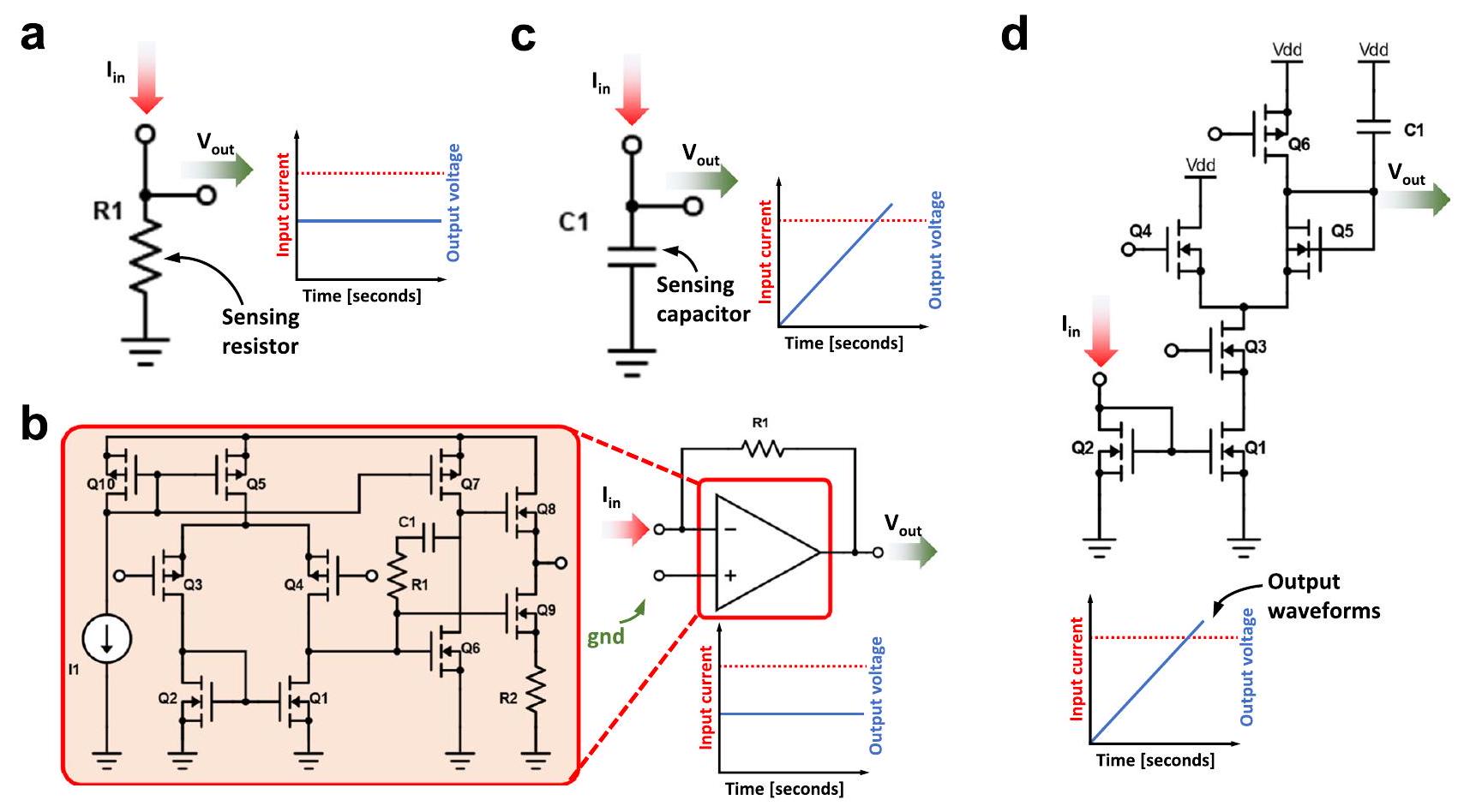
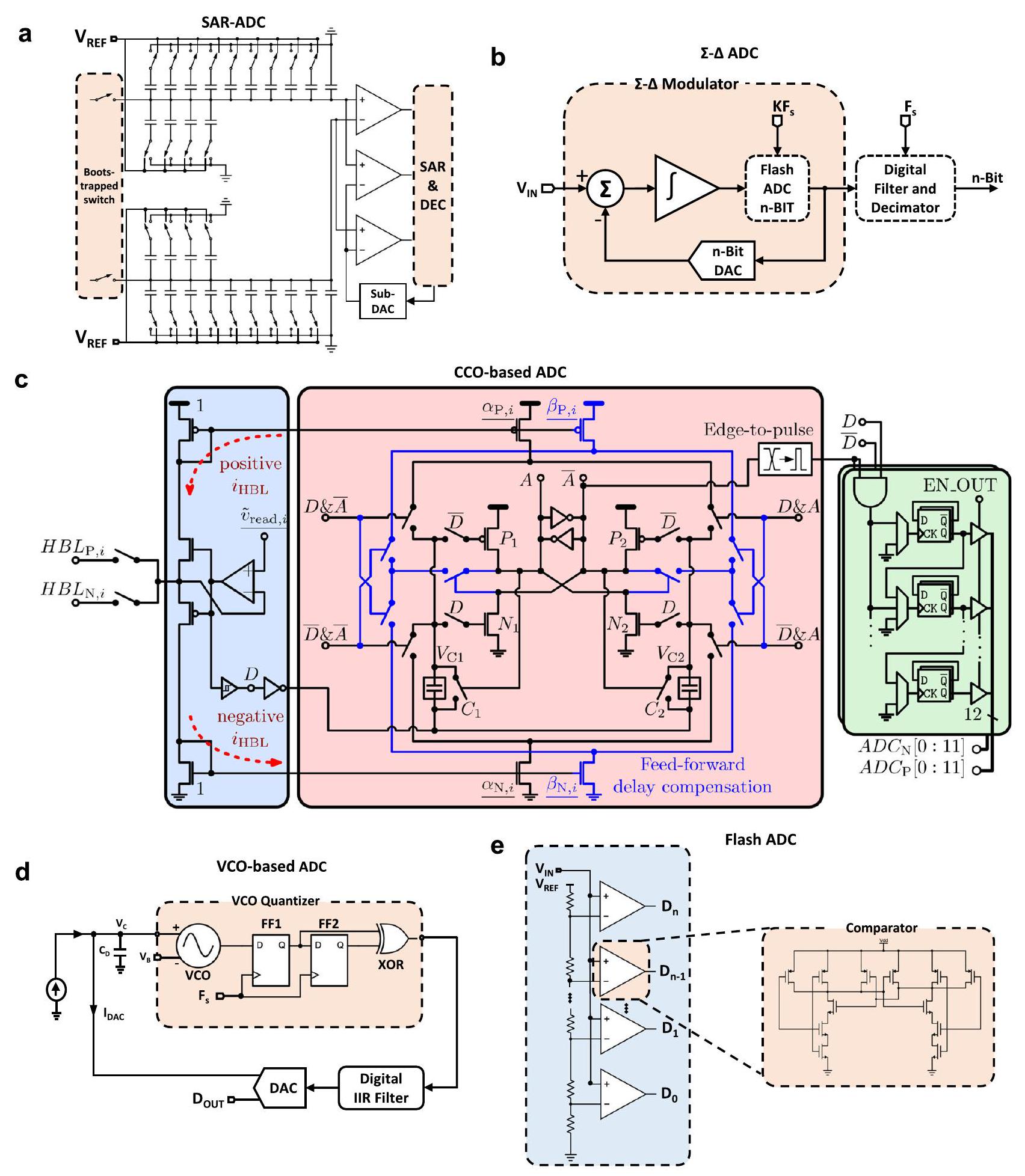
تحت نظام النانو أمبير، تعتبر تكامل الشحنة الخيار الأكثر ملاءمة لتحويل التيار إلى جهد. يمكن تحقيق ذلك باستخدام مكثف. وبالتالي، فإن القياس ليس فوريًا حيث يتطلب وقت تكامل ثابت وقابل للتحكم قبل القياس. لتقليل متطلبات المساحة لمكثف التكامل، يسمح استخدام مقسم التيار بتقليل التيار بشكل أكبر، ومعه، حجم المكثف المطلوب. التبادل في هذه الحالة هو مع الدقة (بشكل رئيسي بسبب عدم تطابق الترانزستورات) ونطاق جهد الخرج الديناميكي.
المخرجات، مضخمة. يجب أن يُلاحظ أنه على الرغم من عدم الضرورة في حالة الشبكات العصبية المنفذة في مجال البرمجيات، في حالة الشبكات العصبية المعتمدة على نوى الميمريستور-VMM، يجب أن تكون عناصر متجهات الإدخال لكل طبقة عصبية ضمن نطاق من الفولتية التناظرية. لهذا السبب، فإن دوال تفعيل ReLU، التي هي بطبيعتها دوال تفعيل غير محدودة. يحتاج إلى تعديل طفيف مع حد أقصى لمنع تغيير الأوزان المشبكية المسجلة في ميمريستور الطبقة العصبية.
يمكن تحقيق جميع هذه الدوال التنشيطية إما في البرمجيات أو في الأجهزة، ولكل تنفيذ مزاياه وعيوبه. في هذه الدراسة، تشير التنفيذات المعتمدة على البرمجيات إلى التصاميم التي يتم فيها حساب دوال التنشيط ومعالجة المخرجات الوسيطة بين طبقات الشبكة العصبية الاصطناعية في وحدة أجهزة منفصلة خارج الشبكة المتقاطعة. يمكن أن تكون هذه الوحدة الأجهزة عبارة عن وحدة معالجة مركزية، أو FPGA، أو متحكم دقيق، أو معالج دقيق، أو لوحة دوائر مطبوعة (PCB) اعتمادًا على كيفية دمج بنية الشبكة المتقاطعة مع وحدات المعالجة الأخرى. تشير التنفيذات المعتمدة على الأجهزة إلى دمج الشبكات المتقاطعة الميمريستيف ووحدات دوال التنشيط في نفس الشريحة. في التنفيذات المعتمدة على البرمجيات، يحتاج مخرج كل عمود من الشبكة المتقاطعة إلى التحويل إلى المجال الرقمي باستخدام محول تناظري إلى رقمي (ADC) (مما يزيد بشكل ملحوظ من المساحة واستهلاك الطاقة) ثم يتم إرساله للمعالجة الإضافية. هذه هي الطريقة الأكثر استخدامًا في النماذج البحثية التي تم تطويرها كأدلة تكنولوجية بسبب مرونتها، حيث يمكن تنفيذ دالة التنشيط وتغييرها ببساطة عن طريق تعديل كود البرمجيات. . في سياق تطوير المنتجات المستقبلية، تم اقتراح الدوائر المتكاملة القابلة لإعادة التكوين (ASICs) لمعالجة الإشارات بعد التحويل من التناظرية إلى الرقمية. وعلى النقيض من ذلك، فإن الدوائر المتكاملة الخاصة (ASIC) –
لا يمكن تغيير تنفيذات دوال التنشيط المستندة إلى الدوائر المتكاملة في نفس الشريحة مثل تقنيات التقاطع بعد تصنيع الدائرة. يمكن تنفيذ مثل هذه الدوال في كل من المجالات الرقمية والتناظرية. يؤدي المعالجة في المجال الرقمي إلى زيادة الحمل الناتج عن محول التناظر إلى الرقمي (كما هو الحال في التنفيذات المستندة إلى البرمجيات) ولكنه يتأثر بشكل أقل بالضوضاء وعدم تطابق الترانزستورات. يتم عرض تنفيذ دالة ReLU المنشطة في المجال الرقمي المدمجة في دائرة الاستشعار في بشكل عام، تتطلب تطبيقات CMOS التناظرية لوظائف التفعيل عددًا أقل من الترانزستورات وتساعد على تجنب التحويل من التناظرية إلى الرقمية في هذه المرحلة. تظهر تطبيقات CMOS التناظرية لوظائف التفعيل في الشكل 9 (انظر الشكل 9أ لوظيفة التفعيل Sigmoid والشكل 9ب لوظيفة التفعيل ReLU). على الرغم من أن مثل هذه التصاميم لا يمكن إعادة تكوينها عند تصنيعها، إلا أن هذه الضعف يتم تعويضه باستهلاك طاقة منخفض بشكل كبير (يُقدّر في المرجع 102 لعنصر CMOS بحجم 65 نانومتر بأنه أقل بحوالي 30 مرة). قدمت المراجع 119 و126 تطبيقات CMOS التناظرية لوظائف التفعيل Sigmoid وReLU وHyperbolic Tangent ضمن الشبكات العصبية الاصطناعية والشبكات التنافسية التوليدية (GAN) على التوالي.
نظرًا لأن الشبكات العصبية الاصطناعية تحتاج إلى عدد كبير جدًا من التنشيطات لتحقيق دقة عالية، فإن استهلاك الطاقة المنخفض لوظائف التنشيط المخصصة المصنوعة من CMOS التناظرية قد لا يزال مفرطًا. يمكن أن يؤدي استخدام جهاز نانو مدمج وفعال من حيث الطاقة ينفذ وظائف التنشيط غير الخطية إلى تعزيز أداء وكثافة تكامل الشبكات العصبية الميمريستية. اقترح المرجع 121 استخدام أكسيد الفاناديوم ( جهاز عازل موت (الذي يتم تسخينه بواسطة فقدان الطاقة جولي) لتحقيق وظيفة ReLU المرغوبة (انظر الشكل 9c)، واقترح المرجع 127 استخدام دليل موجي نانوفوتوني من الليثيوم نيوبيوم ذو فيلم رقيق مُنظم بشكل دوري لتنفيذ ذلك.
الشكل 8 | الدائرة الكهربائية المعادلة للطوبولوجيا المستخدمة لتنفيذ الفرق الرياضي بين إشارتين كهربائيتين. أ بافتراض أن مدخلات الجهد أحادية القطب (أي، إما سلبية أو إيجابية فقط)، يتطلب الأمر أولاً تحويل إشارات التيار إلى جهد ثم إضافة مضخم عمليات في وضع الطرح.
التكوين. إذا كان بالإمكان تطبيق إشارات ثنائية القطب في المدخلات، من خلال تحييد الأوزان المشبكية السلبية بجهد أو قطبية معاكسة، فإن جمع التيارات الناتجة في نقطة مشتركة (قانون كيرشوف للتيار) يحل بالفعل عملية الطرح، ويتطلب الأمر فقط مضخم تحويل التيار إلى جهد واحد لكل عمود.
الشكل 9 | تنفيذات دائرية لوظائف التفعيل التناظرية المستخدمة في الشبكات العصبية الميمريستيفية. تنفيذات كاملة بتقنية CMOS لـ سيغمويد و دوال تفعيل ReLU. تهدف إلى تقليل المساحة المخصصة لدالة التفعيل، يقدم تنفيذًا لـ ReLU يعتمد على جهاز عازل موت
وظيفة في الشبكات العصبية البصرية. على الرغم من أن هذه التصاميم واعدة كحل صغير وفعال من حيث الطاقة لتنفيذ دوال التنشيط، إلا أن تكاملها الفعال مع الدوائر المحيطية الأخرى ومكونات CMOS لا يزال يمثل تحديًا مفتوحًا.

دالة SoftArgMax (الكتلة 8)

بدلاً من دوال التفعيل التي تم وصفها سابقًا، تستخدم الطبقة المشبكية النهائية في الشبكة العصبية الاصطناعية كما تم تغطيته هنا، كتلة مختلفة. في هذه الحالة، من الضروري أن يكون هناك كتلة تكشف عن أي مخرج هو الأكثر نشاطًا في الشبكة المتقاطعة (أي، أي عمود يقود بأعلى).
الكتلة الحالية (غالبًا ما تُسمى دالة SoftArgMax أو دالة تنشيط SoftArgMax) التي تحتوي على عدد من المدخلات يساوي عدد خطوط البت، تقوم بتنفيذ معبر الميمريستور، وتطبق بشكل أساسي المعادلة 10:
الذي يشير إلى أن عنصر من المتجه هو الحد الأقصى بين جميع العناصر لـ وبذلك يحدد نمط الإدخال كعضو في الفئة متجه الإدخال يمثل العارضة
الشكل 10 | تنفيذ تناظري لـ CMOS لنظام الفائز يأخذ كل شيء (WTA)
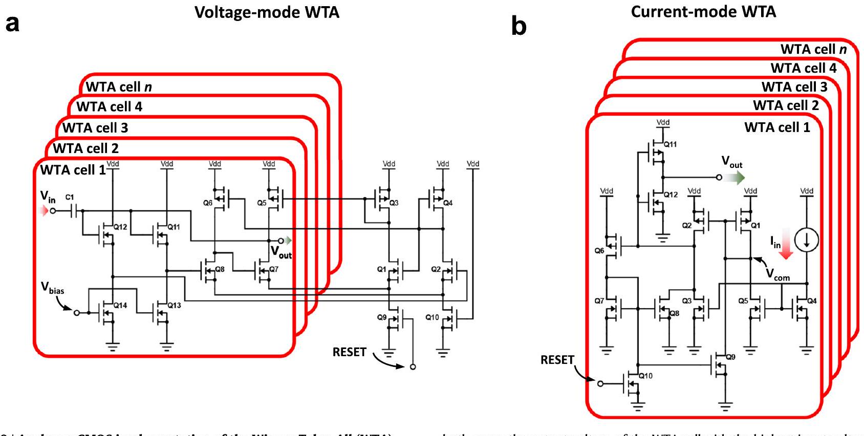
وظيفة. كتلة WTA CMOS مع مدخل جهد . طرف البوابة للترانزستور Q5، وأطراف المصدر للترانزستورات Q6 و Q7 مشتركة بين جميع خلايا WTA. ب كتلة WTA CMOS مع إدخال تيار عقدة هو شائع بين جميع خلايا WTA. في
في كلا الحالتين، يتم دفع جهد الخرج لخلية WTA ذات أعلى جهد/ تيار دخل إلى جهد المرجع الإيجابي. بينما يتم توجيه جهد الخرج للخلايا المتبقية في WTA إلى الأرض. عدد الخلايا في وحدة WTA هو نفس عدد فئات الصور التي يجب التعرف عليها بواسطة الشبكة العصبية الاصطناعية.
المخرجات. يتم تحقيق هذا السلوك من خلال دمج وظيفتين، ودالة السوفتمكس()، الموضحة في المعادلتين 11 و 12، على التوالي.
يمكن أن يُقال إن مثل هذا السلوك (أي تحديد أكبر ناتج من الشبكة) يمكن تحقيقه مباشرة بواسطة دالة argmax() دون الحاجة إلى عملية softmax(). وذلك لأن كما هو موضح في المعادلة 11، فإن argmax() هي عملية تجد الحجة التي تعطي القيمة القصوى من دالة الهدف. لذا، بالنسبة لمسرعات الاستدلال فقط، من المقبول تغذية ناتج دوال التنشيط مباشرة إلى دالة argmax()، متجاوزين دالة softmax(). وقد اقترحت بعض الدراسات تنفيذ دالة argmax() عبر الأجهزة. ، مما قد يكون مفيدًا لتقليل العدد الإجمالي للترانزستورات واستهلاك الطاقة مع زيادة الإنتاجية في نفس الوقت. في هذا الصدد، هناك احتمالان: استخدام كتلة رقمية من نوع CMOS أو لاستخدام كتلة تماثلية من نوع CMOS ، والتي يمكن أن تعمل إما بإدخال تيار أو جهد (انظر الشكل 10أ، ب، على التوالي). لاحظ أن هذه الكتل في الواقع تنفذ ما يسمى وظيفة الفائز يأخذ كل شيء، والتي تستخدم على نطاق واسع في الشبكات العصبية السريعة وخاصة في التعلم التنافسي غير المراقب (يمكن اعتبار ذلك مشابهًا لدالة argmax() ولكن مع إضافة تثبيط جانبي). استخدام كتلة رقمية أبسط وأكثر موثوقية (يمكن كتابتها بسهولة بلغة فيريلوج أو VHDL)، لكنها تقدم العيب الكبير المتمثل في الحاجة إلى محول تناظري رقمي (ADC) عند كل مخرج (أي، عمود) من الشبكة.
ومع ذلك، يُوصى (حتى للاستخدام فقط في الاستدلال) بأخذ دالة softmax() في الاعتبار أيضًا، حيث إنها تحول المتجه الناتج عن دوال التنشيط إلى متجه من الاحتمالات، حيث تكون احتمالات كل قيمة متناسبة مع النطاق النسبي لكل منها.
القيمة في المتجه (مجموع احتمالات جميع العناصر يساوي 1). لاحظ أن يتم تحديد ناتج دالة السوفتمكس () ليس فقط من خلال القيمة ( ) الإدخال ولكن أيضًا بقيمة الآخر المدخلات. علاوة على ذلك، بالنسبة للمسرعات القابلة للتدريب، عادةً ما يكون من غير الممكن حذف دالة softmax()، حيث إنها مطلوبة لحساب دالة الخسارة، التي تحدد الطريقة التي يتم بها تعديل الاتصالات المشبكية. يتم تنفيذ هذه العملية من خلال إعادة نشر تدرج كل دالة رياضية من الشبكة إلى الطبقة السابقة (سيتم وصف تفاصيل هذه الإجراءات بشكل أكبر في قسم تدريب الشبكة العصبية وتحديث الوزن المشبكي (الكتل 2، 11-15): خوارزمية التعلم). نظرًا لأن تدرج الدالة الدالة تكون دائمًا صفرًا، واستخدامها بدون دالة السوفتمكس() سيؤدي إلى عدم تحديث الأوزان المشبكية. تقوم معظم الدراسات بتنفيذ هذه الكتلة عبر البرمجيات. ، الذي يستخدم تمثيلًا رقميًا لإشارة الجهد المقدمة من دالة التفعيل السابقة (المناقشة في قسم دالة التفعيل (الكتلة 7)). تتطلب هذه الطريقة استخدام محول تناظري إلى رقمي (ADC) عند مخرج دالة التفعيل لكل عمود (أجهزة تناظرية). يتم قراءة هذا المتجه الرقمي بواسطة بايثون أو MATLAB روتين يعمل على جهاز كمبيوتر أو FPGA وتم تحديد العنصر الأعلى قيمة. على الرغم من أن هذه الأمثلة هي في الأساس إثباتات لمفهوم تركز على تنفيذ الأجهزة لشبكات الأعصاب الاصطناعية، يمكن القول إن الأنظمة المستقبلية على الرقاقة التي تشمل كل من وحدات الحوسبة في الذاكرة والنوى التقليدية من نوع فون نيومان يمكن أن تعتمد على الأخيرة لتنفيذ وظائف مثل دالة softargmax() على المتجه الرقمي المقدم من وحدات الحوسبة في الذاكرة. لاحظ أنه في بعض الحالات، يتم تنفيذ دالة التفعيل أيضًا رقميًا وبالتالي يتم وضع كتلة محول التناظر إلى الرقمي (ADC) مباشرة بعد إلكترونيات الاستشعار التي تم مناقشتها في قسم إلكترونيات الاستشعار (الكتلة 6).

محولات التناظرية إلى الرقمية (الكتلة 9)

في الحالات التي تكون فيها وحدات تحويل التناظر إلى رقمي (ADCs) مطلوبة (إما بين مخرج الشبكة المتقاطعة وكتلة دالة التفعيل أو بين كتلة دالة التفعيل وكتلة softargmax())، فإن أهم المعايير التي يجب أخذها في الاعتبار هي: (1) دقتها (لأنها تؤثر على الدقة)، (2) تردد العينة ( ) (يؤثر على معدل الإنتاج أو بعبارة أخرى، عدد العمليات في الثانية)، و iii) مساحة السطح على الشريحة
(يحدد المساحة المتاحة من السيليكون المخصصة للأوزان المشبكية، أي هياكل 1T1R، مما يؤثر بالتالي على التكلفة).
دقة المحول التناظري إلى الرقمي المطلوبة لتمثيل جميع المخرجات الممكنة لعملية VMM تعتمد على دقة المدخلات. (دقة DAC)، عدد صفوف الكروس بار ودقة خلايا الوزن (دقة التوصيل)، ويمكن حسابها كـ ceil . على سبيل المثال، الذاكرات الميمريستورية ذات البت الواحد (أوزان ثنائية) والمدخلات الثنائية (بت واحد) في يتطلب العارضة على الأقل دقة 8 بت لتمييز جميع مستويات الإخراج. تتطلب الميمريستورز ذات 5 بت مع نفس أبعاد المتجه والمدخلات الثنائية محول تناظري إلى رقمي بدقة 13 بت، مما يمثل تحديًا تصميميًا خطيرًا للحفاظ على كفاءة استهلاك الطاقة/المساحة، وبالتالي يتطلب تحليلًا دقيقًا للتكلفة والعبء. نظرًا لأن جميع هذه المقاييس مرتبطة ارتباطًا وثيقًا. على سبيل المثال، استنادًا إلى المراجع 150-152، فإن زيادة دقة 1 بت أو زيادة معدل النقل عن طريق مضاعفة تردد العينة يؤدي إلى زيادة في استهلاك الطاقة (خصوصًا لتقنيات CMOS ذات النطاق العالي، حيث يكون استهلاك الطاقة عادةً مقيدًا بالضوضاء الحرارية) ). وبالمثل، فإن تقليل استهلاك الطاقة إلى النصف أو إضافة دقة 1 بت يأتي على حساب المزيد من مساحة السيليكون. علاوة على ذلك، يمكن أن يستهلك محول التناظر إلى الرقمي ما يصل إلى من المساحة على الرقاقة لوحدة الحساب المعتمدة على الشبكة المتقاطعة، بما في ذلك الشبكة المتقاطعة الميمريستيفية والدارات المحيطية، وحتى من الطاقة باختصار، تعتبر محولات التناظرية إلى رقمية (ADCs) عادةً أكبر وأشد كتل الدوائر استهلاكًا للطاقة في شبكة عصبية ميمريستية. لهذه الأسباب، اختار العديد من المؤلفين الذين يركزون على تحسين هياكل خلايا الذاكرة 1T1R استخدام الدوائر المتكاملة الجاهزة، المجمعة في لوحات الدوائر المطبوعة. ، حيث يمكنهم بهذه الطريقة تجنب القيود المفروضة من خلال التوازنات بين الدقة والمساحة والطاقة لمحوّلات التناظرية إلى رقمية. ومع ذلك، من أجل التكامل الكامل على الرقاقة لشبكة عصبية ميمريستيف، يجب تقييم تأثير دقة محوّل التناظرية إلى رقمية على دقة VMM بعناية لتحديد أدنى دقة لمحوّل التناظرية إلى رقمية (وبالتالي المساحة المطلوبة من السيليكون) مع الحفاظ على دقة الشبكة العصبية. .
بشكل عام، يعتمد اختيار بنية محول التناظرية إلى الرقمية (ADC) على احتياجات التطبيق، ويمكن أن يكون التصميم الجيد على مستوى النظام مفيدًا جدًا لتحديد الأداء المطلوب لمحول التناظرية إلى الرقمية. كقاعدة عامة، فإن محولات التناظرية إلى الرقمية ذات الدقة الأعلى تكون أبطأ وأقل كفاءة في استهلاك الطاقة، بينما محولات التناظرية إلى الرقمية ذات تردد العينة الأعلى تكون أقل كفاءة في استهلاك الطاقة وأقل دقة. وبالتالي، إذا كان التركيز منصبًا على تحقيق دقة عالية ( -بت) سجل التقريب المتتالي (SAR-ADC، الشكل 11أ) أو دلتا-سيغما ( -يمكن استخدام محولات التناظرية إلى الرقمية (ADC) كما هو موضح في الشكل 11b) لأنها تتمتع بأحجام صغيرة وأفضل نسبة إشارة إلى ضوضاء وتشويه (SNDR). علاوة على ذلك، فإن محولات التناظرية إلى الرقمية من نوع SAR والمحولات المعتمدة على المذبذبات المتحكم بها (المذبذبات المتحكم بها بالتيار – CCO، انظر الشكل 11c- والمذبذبات المتحكم بها بالجهد – VCO، الشكل 11d-) أكثر ملاءمة لتنفيذات تقنية العقدة الأصغر. . في هذا الصدد، وعلى عكس محولات التناظر إلى الرقمية المعتمدة على VCO الأكثر استخدامًا، فإن محولات التناظر إلى الرقمية المعتمدة على CCO مثل تلك التي اقترحها خدام-الجماعة وآخرون. (انظر الشكل 11ج) يلغي الحاجة إلى دورات تحويل إضافية ويتيح التوازن بين الدقة والكمون. وبالتالي، تسهل هذه الطريقة وجود محول واحد لكل عمود من الأعمدة المتقاطعة، مما يقلل من الكمون الكلي حيث لن تكون هناك حاجة لمشاركة الموارد. على العكس من ذلك، إذا تم التركيز على تردد العينة (مع أوقات قراءة في حدود 10 نانوثانية)، يمكن تطبيق محول تناظري رقمي فلاش منخفض الدقة/عالي السرعة (الشكل 11هـ) عبر التعدد الزمني لتقليل مساحة الرقاقة، حيث إن محولات ADC التي تتمتع بدقة لا تقل عن 8 بت ضرورية لتحقيق أداء عالٍ ( دقة التصنيف في شبكة عصبية ResNET50-1.5 المستخدمة لتصنيف ImageNET قاعدة بيانات أو في شبكة عصبية متعددة الطبقات لتصنيف قاعدة بيانات فحص سرطان الثدي . تتطلب هذه الطريقة استخدام مضاعفات تماثلية (الكتلة 11).
بشكل عام، فإن تقليل عبء العمل على محولات التناظرية إلى رقمية (ADC) هو أحد التحديات الرئيسية في تصميم الأجهزة المعتمدة على الشبكات العصبية القائمة على الميمريستور. إحدى الطرق لمعالجة هذه المشكلة هي الحساب التقريبي أو استخدام محولات ADC بدقة أقل من المطلوبة. . الطريقة الأخرى هي مشاركة محول تناظري إلى رقمي واحد عبر عدة أعمدة أو استخدام محول تناظري إلى رقمي واحد لكل
بلاط العارضة ومع ذلك، يتطلب مشاركة محول التناظرية إلى الرقمية (ADC) مضاعفات إضافية ودارات أخذ العينات والاحتفاظ، كما يزيد من زمن الانتظار. (أي أن المزيد من الوقت مطلوب لمعالجة كل نمط إدخال، مما يقلل من قدرة الشبكة العصبية الاصطناعية). في الشبكات الثنائية، يمكن استبدال محول التناظرية إلى الرقمية بمقارن 1 بت أو مضخم الإشارة متعدد المستويات الشبيه بـ ADC .
بعد تقديم التفاعل بين حجم العبور، دقة متجه الإدخال، مستويات الميمريستور المتاحة ودقة محول التناظرية إلى الرقمية، وكيف تؤثر دقة محول التناظرية إلى الرقمية على مساحة السيليكون، من الجدير مناقشة كيف تضع هذه العوامل قيودًا على كيفية تعامل الشبكة العصبية الميمريستية مع متجهات الإدخال ذات العناصر ثنائية القطب (الإيجابية والسلبية). النهج الواضح هو i) تصميم دوائر محول التناظرية إلى الرقمية بقدرة توفير كل من الفولتية الإيجابية والسلبية. . هذا يعني مضاعفة عدد مستويات خرج DAC، وبالتالي زيادة دقة DAC بمقدار 1 بت (مع الزيادة المرتبطة في تكلفة مساحة السيليكون كما هو موضح في قسم دوائر القيادة المدخلة (الكتلة 4)). يقترح نورازار وآخرون في استخدام محول تناظري بمقاومة خرج منخفضة يتم توصيله بالتناوب إلى خرج DAC أو يتم تجاوزه بناءً على بت الإشارة. ومع ذلك، فإن زيادة دقة DAC بمقدار بت واحد تعني أيضًا زيادة دقة ADC بمقدار بت واحد، حيث يتضاعف عدد المستويات التي يجب تمييزها. لذلك، لا يصبح النظام أكثر حساسية وعرضة للأخطاء فحسب، بل تزداد أيضًا استهلاك الطاقة بشكل أسي مع زيادة دقة DACs و ADCs. بديل لتجنب منطقة السيليكون واستهلاك الطاقة هو تطبيق المدخلات الموجبة والسالبة في مرحلتين قراءة منفصلتين باستخدام فولتages أحادية القطب وطرح نواتج ADC الناتجة عبر المعالجة الرقمية اللاحقة. هذا مشابه لما تفعله منصة ISAAC. يقدم بيانات موقعة بعمق 16 بت إلى المبدل المتقاطع في 16 دورة (بت واحد لكل دورة) بتنسيق مكمل 2. على الرغم من كونه حلاً جذابًا من حيث التكلفة، إلا أن هذه الطريقة تأتي مع تقليل حتمي في معدل النقل حيث يجب استخدام مرحلتين قراءة منفصلتين على الأقل لإكمال منتج VMM واحد.

تدريب الشبكة العصبية وتحديث وزن المشابك (الكتل 2، 11-15)

بصرف النظر عن قيادة إشارات الإدخال والإخراج، من الأساسي ضبط موصلية الميمريستور في الشبكات المتقاطعة إلى القيم المطلوبة لأداء عملية VMM مثمرة. في سياق الشبكات العصبية الاصطناعية، تُسمى عملية تحديد هذه القيم بالتدريب أو التعلم، ويمكن تصنيفها بناءً على i) طبيعة خوارزمية التدريب، و ii) كيفية تنفيذ الخوارزمية المختارة. أولاً، فيما يتعلق بطبيعة خوارزمية التدريب، فإن الطريقة النموذجية للاختيار لمشاكل التصنيف (كما هو الحال في المثال الم discussed هنا) هي التعلم المراقب. التعلم المراقب هو نهج في تعلم الآلة يتم تعريفه من خلال استخدام مجموعات بيانات موسومة، أي أن بيانات التدريب والاختبار مرتبطة بالتسمية الصحيحة. بالنسبة لمجموعة بيانات MNIST، يعني هذا أن صورة تعرض الرقم ‘9’ مرتبطة بعلامة تحمل القيمة ‘9’. من خلال استخدام مدخلات ومخرجات موسومة، يمكن للنموذج قياس دقته والتعلم مع مرور الوقت. تشمل أساليب التعلم الأخرى التعلم غير المراقب. التعلم شبه المراقب، التعلم العدائي، والتعلم المعزز، لكن تنفيذها على الأجهزة أكثر تعقيدًا بكثير. لاحظ أن معظم الأدبيات التي تدعي التعلم غير المراقب باستخدام أجهزة الذاكرة المقاومة استخدمت البرمجيات. ونحن على علم فقط بعدد قليل من الأعمال ، الذي أظهر التعلم غير المراقب القائم على الأجهزة. ثانيًا، وبالنسبة لكيفية تنفيذ خوارزمية التعلم، يمكن القيام بذلك خارج الموقع، أي باستخدام نموذج مثالي للشبكة مكتوب في البرمجيات (كتل ) وكتابة الأوزان المشبكية إلى التوصيلات بمجرد الانتهاء من التدريب أو في الموقع، أي استخدام الشبكة العصبية الميمريستية لحساب عمليات VMM (الكتل 12-15) وتحديث قيم التوصيل تدريجياً خلال عملية التدريب. في الأقسام الفرعية التالية، سيتم مناقشة أساسيات التعلم المراقب، والفرق بين التدريب الخارجي والتدريب في الموقع، وإجراءات ضبط توصيل الميمريستور.
الشكل 11 | مخططات تخطيطية لدارات تحويل التناظرية إلى رقمية المستخدمة تقليديًا في الأدبيات. أ دارة SAR-ADC، ب -ADC، c CCO-ADC، d ADC القائم على VCO و e Flash ADC.
خوارزمية التعلم. خلال التعلم المراقب، نقوم بحساب ناتج الشبكة العصبية الاصطناعية عند تقديم متجه الإدخال من مجموعة بيانات التدريب. ثم يتم مقارنة هذا الناتج مع التسمية المرتبطة بمتجه الإدخال لتحديد خطأ الشبكة. في حالة الشبكة العصبية الاصطناعية مع مدخلات، المخرجات وعدم وجود طبقات مخفية، فإن هذا الخطأ هو دالة لـ أوزان التشابك العصبي للشبكة )، وغالبًا ما يُطلق عليه اسم دالة الخسارة. من أجل تقليل الخطأ، يتم تحديث الأوزان المشبكية بشكل دوري بعد عدد من من متجهات الإدخال (الصور) تُعرض على الشبكة. ثم يمكن فهم عملية التعلم على أنها مشكلة تحسين متعددة المتغيرات، حيث
يجب ضبط أوزان المشابك إلى قيم تقلل من دالة الخسارة. لتحقيق هذا الهدف، يمكن استخدام عائلتين من الخوارزميات: الخوارزميات التي لا تعتمد على التدرج والخوارزميات المعتمدة على التدرج (كما هو موضح في الشكل 12أ). تشمل الطرق التي لا تعتمد على التدرج مثل تحسين سرب الجسيمات الخوارزميات الجينية والتلدين المحاكي تتطلب الخوارزميات مزيدًا من الجهد من وجهة نظر حسابية، وبالتالي، نادرًا ما يتم استخدامها في تدريب الشبكات العصبية الاصطناعية، مما يجعلها خارج نطاق هذه المقالة.
لفهم أساسيات الخوارزميات المعتمدة على التدرج، دعنا نأخذ مثالاً حيث تكون دالة الخسارة دالة ثنائية المتغيرات محدبة.
الشكل 12 | المفاهيم الأساسية لتدريب الشبكات العصبية. أ تنظيم مبسط لأكثر المصطلحات شيوعًا المذكورة في الأدبيات، مع التمييز بين أدوات التدريب المعتمدة على التدرج وأدوات التدريب غير المعتمدة على التدرج. بالنسبة لأدوات التدريب المعتمدة على التدرج، نحن
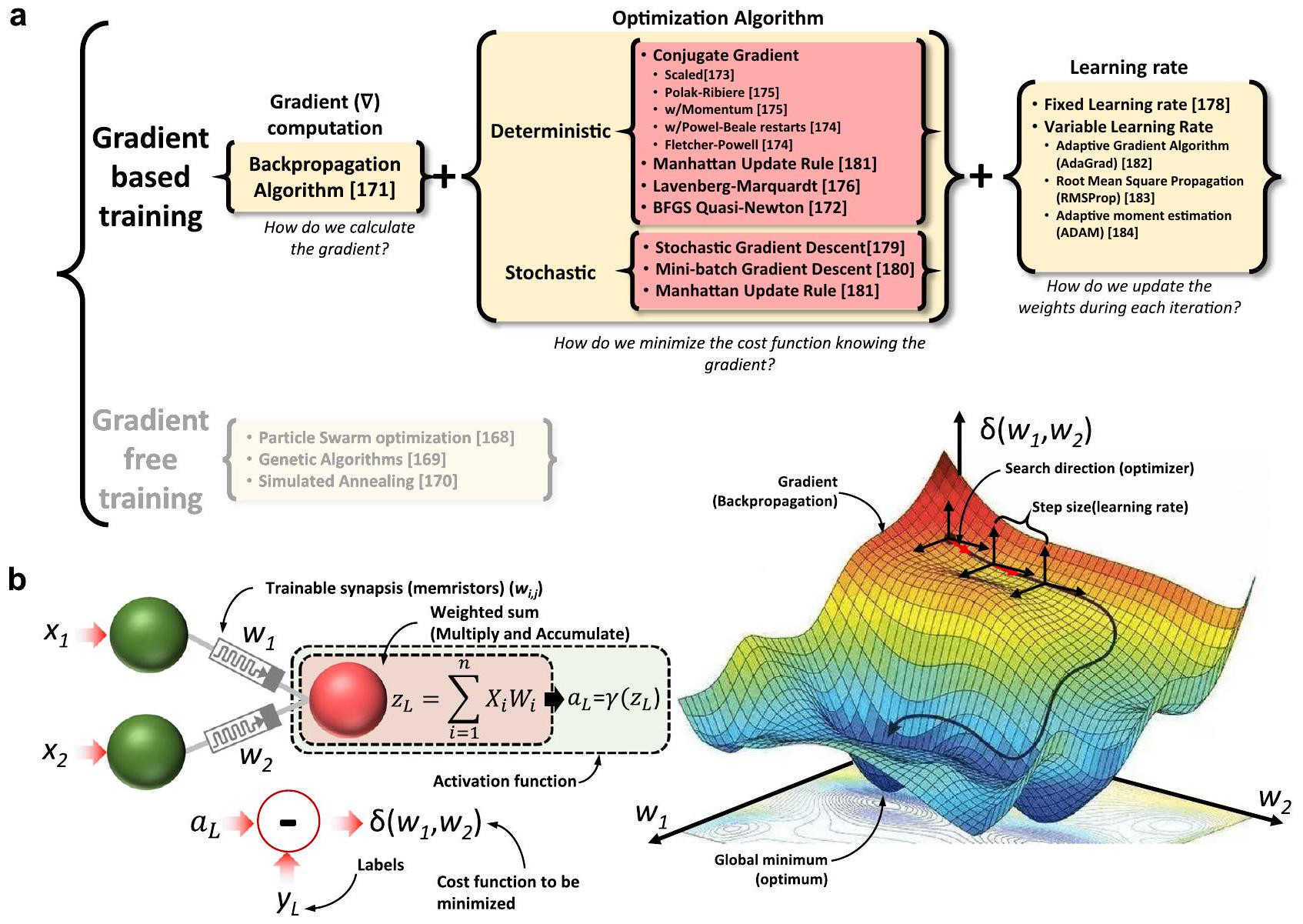
اقترح تنظيمًا للخوارزميات لـ (ط) حساب التدرج، (2) التحسين و (3) معدل التعلم. توضيح لطريقة الانحدار التدرجي، لشبكة عصبية بسيطة تم تدريبها باستخدام التعلم الموجه.
دالة، التي تصف خطأ المخرجات (مقابل التسميات) لشبكة صغيرة تحتوي على مدخلين فقط ومخرج واحد (وبالتالي وزنين عصبيين، كما هو موضح في الشكل 12ب)، وهي . يشير التدرج لمثل هذه الدالة، لنقطة عشوائية ، الاتجاه الذي تزداد فيه الخسارة. باستخدام المعلومات المقدمة من التدرج، يمكننا اتخاذ خطوة بالتقدم عكس التدرج إلى نقطة جديدة وتوقع خسارة أقل. يمكننا بعد ذلك تكرار نفس الإجراء واتخاذ خطوة أخرى في الاتجاه المعاكس للتدرج للنقطة والوصول إلى نقطة جديدة ( ). ستستمر هذه العملية بشكل تكراري حتى نجد مثاليًا أن التدرج هو 0، أو على الأقل أقل من معيار إنهاء. في مجال التدريب الموجه، يُطلق على كل من هذه التكرارات اسم Epoch. في هذه المرحلة (على افتراض أننا نجحنا في تجنب القيعان المحلية) سنكون قد وجدنا القيم لـ و التي تقلل من دالة الخسارة. دالة الخسارة المستخدمة بشكل متكرر لتدريب الشبكات العصبية الاصطناعية هي دالة خسارة الانتروبيا المتقاطعة، والتي تُحسب كما يلي:
حيث هي احتمالية كل فئة لنمط إدخال معين (محسوبة باستخدام دالة softmax)، و هي 1 فقط للفئة ذات الاحتمالية الأعلى و0 بخلاف ذلك. ومع ذلك، عند تعميم هذه المفاهيم على ، تظهر مجموعة من التحديات والأنواع، اعتمادًا على: i) كيفية حساب التدرج المطلوب لدالة الخسارة، ii) كيفية تقييم دالة الخسارة، iii) كيفية تحديد الاتجاه الذي يجب التقدم فيه، و iv) ما هو حجم الخطوة في كل تكرار (من بين عوامل أخرى).
في معظم الشبكات العصبية الاصطناعية، يتم عادةً حساب تدرج دالة الخسارة بواسطة خوارزمية الانتشار العكسي . ثم يمكن تقييم دالة الخسارة بشكل حتمي أو عشوائي. للتقييم الحتمي، يتم تقديم جميع العينات في مجموعة بيانات التدريب إلى الشبكة ويتم حساب الخسارة كمتوسط الخسارة عبر جميع العينات. للتقييم العشوائي، يتم تقدير الخسارة من خلال تقديم متجه إدخال واحد فقط، مما يقدم درجة أعلى من التباين ولكنه يسرع عملية التدريب. بدلاً من ذلك، تم اقتراح استخدام دفعات أيضًا للمساعدة في تقليل التباين، من خلال حساب الخسارة على دفعة من متجهات الإدخال. بعبارة أخرى، تحت التقييم الحتمي لدالة الخسارة ومع الأخذ في الاعتبار مجموعة بيانات MNIST، يفترض كل Epoch تقديم 60,000 صورة. بدلاً من ذلك، خلال التقييم العشوائي، قد يتكون كل Epoch من تقديم صورة واحدة. لاحظ أنه من أجل الشمولية، ولتقديم نظرة عامة كاملة قدر الإمكان للقراء المحتملين الذين ليسوا على دراية بالفعل بمجال التعلم العميق، نقوم بإدراج كل من طرق التحسين الحتمية والعشوائية. ومع ذلك، نادرًا ما تُستخدم الطرق الحتمية (إن وجدت) في أطر التعلم العميق الحديثة، حيث تعتبر المحسنات العشوائية هي المعيار الفعلي لكامل المجتمع. السبب في ذلك هو العبء الحسابي الكبير المتعلق بإرسال مجموعة البيانات بالكامل لحساب التدرج.
لكل حالة (حتمية/عشوائية) هناك خوارزميات مختلفة لتحديد الاتجاه الأمثل الذي يجب البحث فيه عن القيعان بناءً على المعلومات المقدمة من التدرج. هذه هي ما يُعرف بخوارزميات التحسين. بالنسبة لحالة التقييم الحتمي، فإن خوارزميات التحسين الشائعة هي كما يلي: (i) الانحدار التدرجي (الأبسط والأقرب إلى السابق
الشكل -التحقق المتقاطع مع تكرارات تأخذ في الاعتبار خوارزميات تعلم مختلفة. 165,172-178 يتم رسم الدقة التي تم الحصول عليها في كل تكرار مقابل وقت تشغيل وحدة المعالجة المركزية لخوارزمية التعلم عند تدريبها لمجموعة بيانات MNIST لدقتين مختلفتين: و . الصور. على الرغم من أن خوارزمية ليفنبرغ-ماركاردت تظهر أعلى دقة متوسطة، إلا أنها أيضًا الأبطأ في التقارب في تنفيذنا، خاصة عند النظر في الشبكات الكبيرة الحجم،
كما هو مطلوب لتصنيف . الصور. كحل وسط بين الدقة ووقت التعلم، اعتبرنا في المثال الذي سيتم وصفه لاحقًا في هذه المقالة، خوارزمية الانحدار التدرجي المقاييس، حيث إن الفرق في الدقة مع طريقة ليفنبرغ-ماركاردت ليس ذا دلالة إحصائية: أي، قد يكون الفرق الملحوظ بسبب تقلب البيانات في مجموعة بيانات الاختبار.
شرح الفقرة) ونسخها (الانحدار التدرجي مع الزخم )، (ii) نيوتن (معقد تحليليًا، حيث يتطلب بالإضافة إلى التدرج أيضًا مصفوفة هيسيان المرتبطة بدالة الخسارة) وطرق كواسي-نيوتن (التي تعمل على تقريب لمصفوفة هيسيان لتبسيط حساب المشكلة، مثل خوارزمية برويدن-فليتشر-غولدفارب-شانو كواسي-نيوتن ), (iii) طرق الانحدار التبادلي (وسيط بين طرق الانحدار التدرجي وطرق نيوتن التي تتجنب استخدام مصفوفة هيسيان وبدلاً من ذلك تستخدم الاتجاه المترافق للتدرج، مثل الانحدار التبادلي المقاييس ، الانحدار التبادلي مع إعادة تشغيل باول-بيل ، انحدارات فليتشر-باول التبادلية وانحدار بولاك-ريبيير التبادلي ). بدلاً من ذلك، تشمل الطرق الأخرى خوارزمية ليفنبرغ-ماركاردت (تستخدم مصفوفة جاكوب بدلاً من مصفوفة هيسيان)، الانتشار العكسي المرن وخطوة واحدة سيكند ، ولكن هذه أكثر تطلبًا من وجهة نظر حسابية. بالنسبة للتقييم العشوائي، فإن أكثر خوارزميات التحسين شيوعًا هي: i) الانحدار التدرجي العشوائي (المكافئ العشوائي للانحدار التدرجي الطريقة المذكورة سابقًا، على افتراض أن كل Epoch يتكون من متجه إدخال تدريبي واحد فقط) والانحدار التدرجي المصغر (وهو تعميم لطريقة الانحدار التدرجي العشوائي لأحجام Epoch أكبر من 1 وأقل من مجموعة البيانات بالكامل) و ii) قاعدة تحديث مانهاتن (يتم تحديث الأوزان العصبية عن طريق زيادتها أو تقليلها اعتمادًا على اتجاه التدرج، ولكن الخطوة متساوية لجميعها).
حجم الخطوة المتخذة في كل Epoch لتحديث الأوزان العصبية أمر حاسم لأنه يؤثر بشدة على احتمال تقارب الخوارزمية، فضلاً عن وقت التقارب، أي، ستؤدي قيمة خطوة كبيرة إلى عدم تقارب التعلم، بينما ستؤدي القيم الصغيرة إلى وقت تعلم غير مقبول أحيانًا. أبسط نهج هو اعتبار خطوة ثابتة، على الرغم من أن أكثر طرق التعلم تقدمًا تعتمد على خطوة متغيرة يتم ضبطها تلقائيًا بناءً على مجموعة متنوعة من المقاييس. على وجه الخصوص، بالنسبة لحالة التقييم الحتمي لدالة الخسارة، غالبًا ما يتم استخدام الانحدار التدرجي بمعدل تعلم متغير ، ولتقييم دالة الخسارة العشوائية باستخدام دفعة صغيرة من الصور تم استخدام طرق متنوعة، بما في ذلك خوارزمية التدرج التكيفي (أو AdaGrad) ، انتشار الجذر المتوسط التربيعي (أو RMSProp) ، تقدير اللحظة التكيفي (أو Adam) وAdadelta .
تمتلك كل خوارزمية تدريب خصائص رياضية مختلفة، والتي يمكن أن تغير بشكل كبير الدقة ووقت الحساب. لهذا السبب، قبل استخدام أي منها لحساب 60,000 صورة من مجموعة بيانات MNIST، نقوم بإجراء اختبار صغير (يسمى k-fold
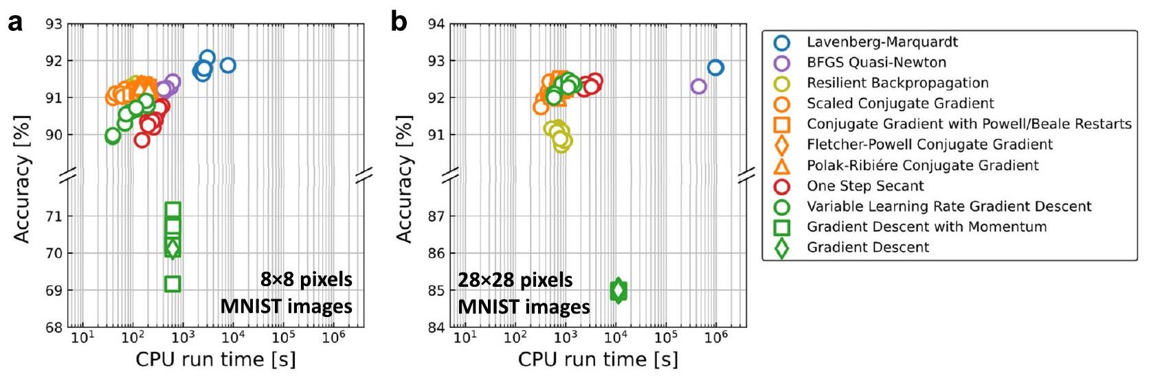
التحقق المتقاطع) حيث يتم تسجيل عدد صغير من صور التدريب والدقة اعتمادًا على خوارزمية التدريب. كمثال، توضح الخوارزمية التكميلية 2 الكود التفصيلي بلغة MATLAB المستخدم لهذا التحقق المتقاطع باستخدام 100 صورة. يتم تقسيم عدد صغير من صور التدريب إلى مجموعات: مجموعات تُستخدم فعليًا لتدريب الشبكة، بينما تُستخدم المجموعة المتبقية للتحقق من نتائج التدريب. ثم يتم تكرار هذه العملية مرات، في كل منها باستخدام مجموعة جديدة من المجموعات المكونة من نفس المجموعة الصغيرة من الصور (100 في هذا المثال) ولكن مختلطة في كل تكرار. الفكرة وراء هذا النهج هي التحقق مما إذا كانت دقة التدريب تعتمد على مجموعة البيانات المستخدمة للتدريب أم لا. في هذا المثال، قسمنا الـ 100 صورة إلى 5 مجموعات ( )، مما أدى إلى 80 صورة للتدريب و20 للتحقق (وهي مختلفة في كل تكرار)، وتم تسجيل دقة الشبكة العصبية الاصطناعية في كل تكرار ( في هذا المثال) لكل خوارزمية تدريب. من أجل الاختصار، اعتبرنا فقط الخوارزميات للتقييم الحتمي لدالة التكلفة المقدمة في صندوق أدوات التعلم العميق في MATLAB. وهذا يعني في المجموع 110 تدريبات لـ 100 صورة. تم الإبلاغ عن نتائج هذه الاختبارات في الشكل 13أ، ب، الذي يظهر أن خوارزميات التعلم Scaled Conjugate Gradient وLevenberg-Marquardt توفر أعلى دقة؛ ومع ذلك، فإن الأولى أسرع بكثير، ولهذا السبب تم اختيارها لهذا المثال. من الواضح أيضًا من الشكل 13أ، أنه بخلاف الدقة المنخفضة، فإن الدقة التي تم الحصول عليها باستخدام Gradient Descent with Momentum تعتمد بشكل كبير على مجموعات بيانات التدريب والاختبار. التفاصيل الإضافية المتعلقة بكل خوارزمية تدريب تتجاوز نطاق هذه المقالة، حيث نركز على تنفيذ الشبكة العصبية الاصطناعية المعتمد على التقاطع.
بعد التحقق، يتم إجراء التدريب الحقيقي باستخدام 60,000 صورة تدريب و10,000 صورة اختبار باستخدام خوارزمية Scaled Conjugate Gradient. يتم عرض كود MATLAB المستخدم لتدريب شبكة عصبية اصطناعية تحتوي على شبكة عصبية أحادية الطبقة (SLP) باستخدام صور MNIST التي تم تصغيرها إلى في الخوارزمية التكميلية 3؛ يوضح الكود كل من إنشاء الشبكة العصبية الاصطناعية والتدريب. يمكن تقييم جودة عملية التدريب من خلال معايير مختلفة (انظر التعريفات في الجدول 2)، والتي يمكن استخدامها أيضًا لتحديد نقطة توقف لإجراء التدريب. هذا أمر حاسم لأنه إذا تم اعتبار عدد قليل جدًا من التكرارات خلال مرحلة التدريب، فقد لا تتناسب الشبكة العصبية الاصطناعية مع بيانات التدريب، ولا تتعرف بشكل صحيح على أنماط الإدخال (حتى خلال مرحلة التدريب). على العكس من ذلك، فإن التدريب المفرط للشبكة العصبية الاصطناعية يؤدي إلى الإفراط في التكيف مع بيانات التدريب، والتي على الرغم من التعرف بدقة على صور التدريب، تقلل من قدرة الشبكة العصبية الاصطناعية على التعرف بشكل صحيح على أنماط الإدخال غير المرئية (المستخدمة خلال مرحلة الاختبار).
الجدول 2 | قائمة المقاييس المستخدمة لتقييم الشبكات العصبية الاصطناعية المستخدمة في تصنيف الأنماط
المقياس التعبير المعنى القابلية للتطبيق أمثلة
الدقة نسبة الأنماط المصنفة بشكل صحيح بالنسبة لعدد الأنماط الكلي لتحديد أداء الشبكة العصبية الاصطناعية لا ينطبق
الحساسية (تسمى أيضًا الاسترجاع) نسبة بين عدد ما تم التعرف عليه بشكل صحيح على أنه إيجابي إلى عدد ما كان إيجابيًا بالفعل أماكن حيث تكون تصنيفات الإيجابيات ذات أولوية عالية فحوصات الأمان في المطارات
الخصوصية نسبة بين عدد ما تم تصنيفه بشكل صحيح على أنه سلبي إلى عدد ما كان سلبيًا بالفعل أماكن حيث تكون تصنيفات السلبيات ذات أولوية عالية تشخيص حالة صحية قبل العلاج
الدقة
TP
عدد ما تم تصنيفه بشكل صحيح على أنه إيجابي من بين جميع الإيجابيات لا ينطبق كم عدد الذين قمنا بتصنيفهم كمرضى سكري هم في الواقع مرضى سكري؟
درجة F1 إنها مقياس لأداء قدرة تصنيف النموذج لا ينطبق تعتبر درجة F1 مؤشرًا أفضل لأداء المصنف من مقياس الدقة العادي
معامل K
الدقة العشوائية
100-الدقة العشوائية
تظهر النسبة بين دقة الشبكة ودقة العشوائية (في هذه الحالة، مع 10 فئات مخرجات، ستكون الدقة العشوائية 10%) لا ينطبق لا ينطبق
الانتروبيا المتقاطعة
حيث، هي 1 إذا كانت العينة تنتمي إلى الفئة و
0 خلاف ذلك، و هي الاحتمالية التي تتنبأ بها الشبكة العصبية الاصطناعية للعينة التي تنتمي إلى الفئة
الفرق بين القيمة المتوقعة من قبل الشبكة العصبية الاصطناعية والقيمة الحقيقية لا ينطبق لا ينطبق
كمثال، يظهر الشكل 14 المقاييس للتدريب المستمد من الخوارزمية التكميلية 3. الشكل الأكثر شيوعًا هو دقة الاستدلال (انظر الشكل 14أ)، وهي النسبة بين عدد الصور المصنفة بشكل صحيح، بالنسبة لعدد الصور الكلي المعروض على الشبكة العصبية الاصطناعية في كل تكرار (غالبًا ما يسمى عصر). مقياس شائع آخر هو مصفوفة الالتباس (انظر الشكل 14ب)، التي تعرض قدرة الشبكة العصبية الاصطناعية على ربط كل نمط إدخال بفئته المقابلة (في هذا المثال رقم من 0 إلى 9) وتسمح بتمثيل دقة الاستدلال رسوميًا لكل إدخال ممكن. أيضًا، فإن دالة الخسارة المستخدمة في التدريب هي مقياس حرج. واحدة من أكثر دوال الخسارة استخدامًا هي الانتروبيا المتقاطعة (انظر الشكل 14ج والجدول 2)، والتي يمكن حسابها كفرق بين القيمة المتوقعة من قبل الشبكة العصبية الاصطناعية والقيمة الحقيقية. وأخيرًا وليس آخرًا، تشمل المقاييس الأخرى ذات الصلة الحساسية (الشكل 14د)، الخصوصية (الشكل 14هـ)، الدقة (الشكل 14و)، درجة F-1 (الشكل 14ز) ومعامل K (الشكل 14ح)، التي تم تقديم تعريفها في الجدول 2، من حيث الإيجابيات الحقيقية (TP، الصور من الفئة المصنفة كأعضاء في الفئة )، السلبيات الحقيقية (TN، الصور التي ليست أعضاء في الفئة والتي لم يتم تصنيفها كفئة )، الإيجابيات الكاذبة (FP، الصور التي لا تنتمي إلى الفئة ولكن تم تصنيفها كفئة ) والسلبيات الكاذبة (FN، الصور التي تنتمي إلى الفئة ، ولكن لم يتم تصنيفها كفئة ). في خوارزميات التصنيف الخاضعة للإشراف، يتم استخدام مقياس الانتروبيا المتقاطعة كدالة خسارة يجب تقليلها خلال مرحلة التدريب.
من المهم التأكيد على أن المقاييس التي تم إنشاؤها بواسطة البرنامج (MATLAB، Python) خلال مرحلة التدريب حتى هذه النقطة ليس لها علاقة بالميمريستور أو مصفوفات التقاطع. نلاحظ أن بعض المقالات التي تركزت على تصنيع وتوصيف الأجهزة على مستوى واحد/قليل من الميمريستور ، تقدم أيضًا بعض المقاييس التي تم إنشاؤها بواسطة عملية تدريب الشبكة العصبية الاصطناعية المعتمدة على البرمجيات (المماثلة لتلك الموجودة في الشكل 14) من أجل الادعاء بأن أجهزتهم تظهر إمكانات للتطبيقات العصبية. هذه ليست ممارسة موصى بها ويجب تجنبها دائمًا، حيث أن النماذج المعنية في هذه الحالات تحتفظ بارتباط ضئيل مع الأجهزة المصنعة، مما يؤدي إلى مقاييس أداء غير واقعية.
التدريب خارج الموقع مقابل التدريب في الموقع. بالنسبة للتدريب خارج الموقع، يتم إدخال الصور المصغرة في شبكة عصبية اصطناعية تعتمد على البرمجيات بحجم . يقوم البرنامج بحساب الأوزان المشبكية التي تقلل من دالة الخسارة من خلال تطبيق الخوارزمية المختارة (الموصوفة في القسم الفرعي السابق)، إما لعدد معين من العصور أو حتى تكون دالة الخسارة أقل من عتبة معينة. ثم، يتم تسجيل الأوزان المشبكية (الكتلة 11) في مصفوفة التقاطع الميمريستية باستخدام نهج WriteVerify (الكتلة 12-14، الموصوفة في القسم الفرعي التالي). يتمتع التدريب خارج الموقع بميزة الحاجة إلى القليل/عدم وجود عبء دائري لإجراء اختبارات سريعة لأداء تصنيف الشبكة، وقد جعل من الممكن تقييم أداء مصفوفات التقاطع الميمريستية المصنوعة في المنزل . لاحظ أنه في أبسط تنفيذ لها، تؤدي عدم المثالية في مصفوفة التقاطع الميمريستية إلى تدهور دقة النتائج التي تم الحصول عليها مع الشبكات العصبية الميمريستية المدربة خارج الموقع. لتجنب فقدان هذه الدقة، تم اقتراح طرق تدريب مدركة للأجهزة، حيث يتم دمج عدم المثالية للأجهزة أثناء التدريب في الأدبيات .
يخزن التدريب في الموقع ويحدث الأوزان المشبكية (الكتلة 15) مباشرة في الميمريستورات، ويقوم بإجراء الحسابات (على سبيل المثال، التمريرات الأمامية) في المكان الأصلي حيث يتم تخزين معلمات الشبكة العصبية، مما له العديد من المزايا. على سبيل المثال، يتجنب الحاجة إلى تنفيذ نظام مكرر في أجهزة الكمبيوتر الرقمية، كما في مخططات التدريب خارج الموقع، مما يعزز بشكل كبير كفاءة المساحة/الطاقة للنظام من خلال القضاء على عنق الزجاجة بين المعالج والذاكرة في أجهزة الكمبيوتر الرقمية ويتجنب عملية التعيين. والأهم من ذلك، أن التدريب في الموقع مع التراجع قادر على ضبط معلمات الشبكة بشكل ذاتي لتقليل تأثيرات عدم المثالية الحتمية للأجهزة (مثل مقاومة الأسلاك، عدم تماثل الأجهزة التناظرية، الميمريستورات غير المستجيبة،
الشكل 14 | الأرقام النموذجية المستخدمة لتحديد أداء الشبكات العصبية الاصطناعية المخصصة للتعرف على الأنماط. في هذه الحالة، تم رسمها كدالة لعدد دورات التدريب. أ الدقة، ب مصفوفة الالتباس، ج دالة الخسارة (الانتروبيا المتقاطعة)، د الحساسية، هـ الخصوصية، و الدقة، ز درجة F1، ح معامل k.
انحراف الموصلية والتغيرات في برمجة الموصلية) دون أي معرفة مسبقة بالعتاد ومع ذلك، هناك عاملان يعقدان تنفيذ التدريب في الموقع. أولاً، تتطلب الأجهزة المعنية دقة عالية لبرمجة تحديث الوزن بدقة وقدرة عالية على التحمل بسبب عمليات SET/RESET المتكررة خلال عملية التدريب. يمكن أن يؤدي التدريب بدقة مختلطة، الذي يجمع تحديث الوزن في البرمجيات ويقوم بتحديث أجهزة الميمريستور فقط عندما يتجاوز القيمة المجمعة دقة البرمجة، إلى تخفيف كبير لمتطلبات دقة تحديث التوصيل والقدرة على التحمل، ويسمح بتحقيق دقة قابلة للمقارنة مع البرمجيات. . ثانياً، لاستغلال التعلم في الموقع بشكل كامل في تطبيق عملي، من الضروري ليس فقط تنفيذ VMM في الشبكة المتقاطعة، ولكن أيضاً تنفيذ خوارزمية التعلم على الشريحة. في هذا الصدد، التحدي مزدوج: من ناحية، يتطلب نضوجاً عالياً لتقنية الميمريستور المعنية. وهذا يعني أن مجموعة الميمريستور يجب أن تكون قادرة على الاندماج بأمان في الجزء الخلفي من عملية CMOS دون التأثير على الجزء الأمامي. هذه بالفعل تعتبر قيداً للعديد من الدراسات البحثية التي تتضمن مواد وعمليات غير ملائمة لمجموعات CMOS التقليدية. من ناحية أخرى، وبشرط أن يتم تلبية الشرط السابق، فإن تطوير الإلكترونيات اللازمة على الشريحة ليس بالأمر السهل ويفترض تكلفة كبيرة لبرامج البحث. وبالتالي، فإن الحل البديل هو تنفيذ إلكترونيات الدوائر المحيطية خارج الشريحة باستخدام مكونات جاهزة. بهذه الطريقة، يمكن تقييم تأثير الإلكترونيات التناظرية بشكل أكثر واقعية دون تكبد نفقات باهظة، مما يؤدي إلى مجموعة متنوعة من النماذج الأولية التي يتم فيها تنفيذ الدوائر اللازمة للتراجع خارج الشريحة، وهو نهج هنا يُطلق عليه اسم التعلم الجزئي في الموقع. هذه هي حالة المراجع. . في جميع هذه الأعمال، يتم تنفيذ عملية VMM المطلوبة للتمرير الأمامي بواسطة مصفوفة الميمريستور، ويتم تسجيل المتجهات الناتجة الرقمية بواسطة لوحة الدوائر المطبوعة الخاصة بالاستحواذ. ثم يتم معالجة المتجه الناتج بواسطة خوارزمية التدريب في البرنامج لتحديد كيفية تحديث الوزن المشبكي بعد كل حقبة تدريبية. من خلال هذا النهج الجزئي، تم إثبات التدريب في الموقع لمسرعات الشبكات العصبية الاصطناعية والشبكات العصبية الاصطناعية ذات التمرير الأمامي من الشبكات العصبية المتصلة بالكامل إلى الشبكات العصبية التلافيفية (CNNs)، مما يظهر قدرة محسنة على تصنيف الأنماط. على الرغم من أن طرق التعلم الموصوفة في الفقرة السابقة صالحة أيضًا لـ
في تدريب الوضع الحالي، كانت الممارسة المعتادة المبلغ عنها في الأدبيات لهذا النوع من التدريب هي استخدام ما يُعرف بقانون تحديث مانهاتن. أو خوارزمية الانحدار العشوائي .
برمجة الوزن. مرحلة برمجة الوزن هي العملية التي يتم من خلالها تحديث الموصلية (أي الأوزان) للذاكرات الميمريستورية إما لتطابق الأوزان المدربة خارجياً أو من خلال اتباع القواعد المحددة لخوارزمية التعلم لأساليب التعلم في الموقع. يتم تنفيذ عملية تحديث الوزن عن طريق تطبيق نبضات جهد أو تيار على الذاكرات الميمريستورية (الكتل 13 و 14)، وفقاً لعملية الكتابة والتحقق (أو ضبط الحلقة المغلقة). أو الكتابة بدون تحقق (أو ضبط الحلقة المفتوحة) الفرق بينهما هو أنه في نهج الكتابة والتحقق، يتم تطبيق نبضة قراءة بين نبضات الكتابة المتعاقبة، لقياس التوصيلية التي تم تحقيقها بعد نبضة الكتابة وتحديد ما إذا كانت تحديث الوزن قد اكتمل، أو إذا كانت هناك حاجة إلى نبضات إضافية أو أعلى. عندما تتطلب توصيلية الميمريستور في الشبكة تقوية متكررة، فإن طريقة الكتابة بدون تحقق هي الأنسب لأنها تحافظ على سرعة التشغيل العالية وتبقي العبء على الأجهزة في الحد الأدنى، على حساب تحمل خطأ كتابة أعلى. على العكس، إذا كانت controllability الأفضل لقيم التوصيلية مفضلة على سرعة التشغيل العالية أو إذا لم يكن التحديث المتكرر للتوصيلية متطلبًا رئيسيًا، فقد تم الإشارة إلى أن الكتابة والتحقق هي الخيار الأفضل.
تسمى العمليات التي يتم من خلالها زيادة وتقليل موصلية الميمريستور بالتعزيز والاكتئاب، على التوالي، وقد تم ملاحظتها عند تطبيق تسلسلات مختلفة من نبضات الجهد. إنها مرتبطة بتعديل خاصية واحدة أو بعض الخصائص للمواد في الجهاز الميمريستيف (مثل، موقع الذرات، الطور، الاستقطاب، الدوران، وما إلى ذلك). لقد راجعت مجموعة كبيرة من الدراسات الآليات المختلفة للتبديل في الأجهزة الميمريستيف. لذلك لن نتعمق أكثر في هذه المسألة. ولكن الشيء المهم من وجهة نظر الشبكات العصبية الاصطناعية هو أن تغيير الموصلية خلال عمليات التعزيز والاكتئاب يكون في معظم الحالات غير خطي. يمكن أن تساعد إدخال نبضات غير متطابقة في تقليل عدم الخطية، وقد توصلت بعض الدراسات إلى عملية تعزيز واكتئاب قريبة من الخطية ومتوازنة من خلال تطبيق نبضات إيجابية متزايدة ونبضات سلبية متناقصة، على التوالي. في بنية 1T1R، يوفر الطرف الثالث (أي، بوابة الترانزستور) تحكمًا أعلى في ضبط موصلية الميمريستور. .
ومع ذلك، فإن استخدام نظام نبضات متغيرة يتطلب عادةً نهج كتابة-تحقق لتحديد حالة التوصيل أولاً ثم تطبيق نظام النبضات الصحيح على الجهاز، أو تخزين سعة النبضات خارجيًا لتطبيقها على كل وزن. لهذا السبب، تم إثبات هذه الأساليب في الغالب لتحديث الوزن للأجهزة المعزولة، مع وجود عدد قليل فقط من الأمثلة على الأساليب المدمجة على الشريحة. . كما أن كلا الخيارين يزيدان حتمًا من تعقيد الدوائر الطرفية بالإضافة إلى الكمون والطاقة، مما يجعل تحديث الوزن في الموقع باستخدام أنظمة النبض المتغيرة غير فعال تمامًا مثل القيام بذلك خارجيًا بطريقة رقمية. وبالتالي، يتم استخدام الأساليب التي يتم فيها تطبيق نبضات متطابقة على الأجهزة عند تصميم الدوائر العصبية التي تهدف إلى كفاءة الطاقة. ومع ذلك، فإن طريقة الكتابة والتحقق التقليدية تفرض متطلبات كبيرة على كتلة قياس التيار، التي يجب أن تكون دقيقة سواء لقياس التيار من خلال جهاز واحد (خلال مرحلة تحديث الوزن) أو من خلال العمود بأكمله (خلال الاستدلال). في هذا الصدد، تم اقتراح نهج جديد واعد مؤخرًا من قبل بوشيل وآخرين. ، بهدف تحسين طريقة الكتابة-التحقق بشكل أكبر. في هذه النسخة، بدلاً من تحديث كل وزن بهدف الوصول إلى هدف موصلية معين، يتم تحديث الأوزان من أجل تقليل خطأ ناتج VMM. وبالتالي، فإن متطلبات التصميم لدارات قياس التيار أقل صرامة.

تصنيع/دمج شريحة الشبكة العصبية الاصطناعية

يمكن تصنيع مصفوفات العوارض العرضية لأجهزة الميمريستيف المعدنية/العازلة/المعدنية ذات الطرفين بسهولة باستخدام تقنيات الطباعة الحجرية والترسيب القياسية؛ وقد تم تحقيق ذلك بسهولة من قبل مجموعات متعددة. تفضل بعض المجموعات دمج ترانزستور في سلسلة مع كل خلية MIM للحصول على تحكم أفضل في التيارات عبر الجهاز (أي تحسين قابلية التحكم في التوصيل وتقليل تيارات المسار الخفي). عادةً ما تكون الممارسة الشائعة هي تصنيع الترانزستورات في شركة وتركيب خلايا MIM فوق الترانزستورات في الموقع على الرقاقة المستلمة (بعد إزالة فيلم الحماية أو الأكسيد الطبيعي، بحيث يمكن الوصول إلى أطراف الترانزستور) .
ثم يتم دمج العارضة (الكتلة 5 في الشكل 2) في الشبكة العصبية الاصطناعية عن طريق توصيل كل واحد من مدخلاتها إلى محول رقمي تماثلي (الكتلة 4، لتطبيق الجهد التماثلي الذي يمثل السطوع أو اللون لكل بكسل من الصورة)، وكل واحد من مخرجاتها إلى مضخم تيار (الكتلة 6، لتحويل التيار الناتج إلى جهد)؛ ثم يتم تغذية الجهد التماثلي الناتج من مضخم التيار إلى الكتلة التي تنفذ دالة التنشيط (الكتلة 7) ودالة softargmax() (الكتلة 8). للاستفادة الكاملة من مزايا مصفوفة العارضة من الميمريستور، سيكون السيناريو الأفضل هو دمج الكتل CMOS (DAC، TIA، ADC) بالكامل على الشريحة. ومع ذلك، لتجنب تصنيع الدوائر المتكاملة البطيء والمكلف (أي، عمليات الطباعة)، تفضل معظم المجموعات بناء كتل CMOS خارج الشريحة. في السطور التالية، نذكر الاستراتيجيات الأكثر شيوعًا المتبعة لتنفيذ الأجهزة للشبكات العصبية الميمريستية، من الأكثر بدائية إلى الأكثر تعقيدًا:
أبسط نهج هو ضرب تماثلي متسلسل (صفًا بصف) مع مدخلات ثنائية. الذي لا يقوم بعملية VMM تماثلية لأن عملية الضرب تتم في كل ميمريستور، لكن التجميع يتم بواسطة دوائر خارجية. ثم، تم إثبات VMM التماثلي لكل من المدخلات الثنائية والأوزان. بالإضافة إلى المدخلات الثنائية والأوزان التناظرية/متعددة المستويات . في كلتا الحالتين، يتم تقليل تعقيد الدائرة قليلاً من خلال تجنب استخدام محولات الرقمية إلى التناظرية (DACs) في مدخلات الشبكة المتقاطعة. المزايا الخاصة بكل حالة هي في حالة الأوزان الثنائية تعديل موصلية أبسط وأكثر موثوقية، وفي حالة الأوزان التناظرية/متعددة المستويات عدد أكبر من البتات لكل مشبك عصبي. ومع ذلك، في كلتا الحالتين، فإن الفولتages المدخلة الممكنة هي فقط 0 أو ، مما يعني أنه يمكنه العمل فقط مع لونين لكل بكسل (أي، صور بالأبيض والأسود). إن استخدام إشارات الإدخال التناظرية/ متعددة المستويات مفيد لمعالجة الصور التي تحتوي على المزيد من الألوان لكل بكسل، ولكنه يتطلب وجود محول رقمي تماثلي (DAC) لكل خط كلمة. عندما يكون عدد المستويات
عندما تزداد إشارة الإدخال، تزداد أيضًا تعقيد دائرة المحول الرقمي إلى التناظري (ومعها، استهلاك الطاقة والمساحة). النهج الأكثر شيوعًا في هذا السياق هو استخدام محول رقمي إلى تناظري خارجي جاهز لتشغيل المدخلات التناظرية. والتي تتكامل مع بقية الدائرة (أي، مصفوفة الميمريستور) في لوحات الدوائر المطبوعة. من أجل نهج VMM كامل الأجهزة وكامل التناظرية، من الضروري دمج DAC و ADCs ومصفوفة الميمريستور على نفس شريحة السيليكون. عادة ما تكون هذه العملية محدودة بمتطلبات المساحة لهذه الكتل التناظرية. كانت هناك حل متكرر فعال من حيث التكلفة يتمثل في استخدام عدد أقل من DACs ومشاركتها بين صفوف مختلفة من خلال إضافة طبقة من المMultiplexors التناظرية بين DACs ومدخلات خطوط الكلمات. . مع هذا النهج (الذي يمكننا الإشارة إليه كمدخلات تماثلية متعددة الأوقات على الشريحة – أوزان تماثلية/متعددة المستويات)، يتم تقسيم عملية VMM المعطاة في تتم إضافة عمليات VMM الفرعية المختلفة والنتائج الجزئية لكل منها في النهاية، مما يوفر المساحة والطاقة على حساب تقليل الإنتاجية. أخيرًا، تستفيد النماذج الأولية الأكثر تقدمًا من نظام ترميز الوقت، الذي يبسط تصميم DAC ويسمح بوجود DAC واحد لكل قناة، دون فقدان دقة المتجه المدخل. . نحن نطلق على هذه الحالة اسم إدخال متعدد البت على الشريحة – أوزان تناظرية/متعددة المستويات. في الجدول 3، نقدم مقارنة موجزة بين أكثر هياكل الشبكات العصبية الهجينة RRAM/CMOS تقدمًا والإصدارات الكاملة من CMOS المتاحة تجاريًا. كما هو موضح، فإنها تحقق أداءً مشابهًا من حيث معدل النقل، ولكن في بعض الأحيان لا تزال الهياكل الهجينة RRAM/CMOS محدودة باستهلاك المساحة الكبير لدارات تحويل التناظرية إلى رقمية.
في جميع الحالات، تكون الأداء (المحدد من حيث الدقة، والعمليات في الثانية، واستهلاك الطاقة، ومتطلبات المساحة) محدودًا بالخصائص الكهربائية لأجهزة الميمريستور (العيوب غير المثالية مثل تأثير المسار الخفي، والضوضاء، ومقاومة الخط التي سيتم مناقشتها لاحقًا في المقال) والدائرة المحيطية المتاحة بتقنية CMOS. لتحقيق أقصى أداء ممكن مع تقنية الميمريستور المعطاة، من الضروري اختيار الدوائر المحيطية المناسبة (الموصوفة في قسم هيكل الشبكات العصبية المعتمدة على الميمريستور). نظرًا لأن تصميم وإخراج الدوائر المتكاملة المخصصة بتقنية CMOS يستغرق وقتًا طويلاً ويكون مكلفًا، فمن الضروري تقليل عدد دورات التصميم-التصنيع-القياس إلى الحد الأدنى. لتحقيق هذا الهدف، يعتمد مصممو الشرائح على المحاكيات، التي يمكنها تقديم تقدير لأداء الدائرة المتكاملة وحتى اكتشاف المشكلات المحتملة في التصميم قبل مرحلة الإخراج.

محاكاة الشبكات العصبية الميمريستية

تعتبر المحاكيات أداة أساسية تُستخدم من نمذجة الأجهزة على مستوى منخفض إلى استكشاف الأنظمة على مستوى عالٍ. توضح الشكل 15 المستويات الخمسة الرئيسية للتجريد التي تُستخدم فيها المحاكيات، بينما تقدم الجدول 4 قائمة شاملة بالبرمجيات التي تم اعتبارها في الأدبيات لمحاكاة الشبكات العصبية الاصطناعية والشبكات العصبية الاصطناعية الميمريستيفية. بشكل عام، يجب أخذ التوازنات بين سرعة المحاكاة والدقة (أي مدى قرب المحاكاة الكهربائية من القياسات الحقيقية للدائرة) في الاعتبار. من ناحية، تتطلب المحاكيات على مستوى الشبكة العصبية أداءً عاليًا بسبب الكمية الكبيرة من العمليات (مثل VMM، تسطيح الأنماط، دوال التنشيط) وبالتالي، فهي ليست محسّنة من حيث دقة المحاكاة. من ناحية أخرى، يجب أن تحسب المحاكيات التي تُجرى على مستوى الجهاز نماذج فيزيائية دقيقة لتقليد سلوك الأجهزة، مما يبطئ سرعة المحاكاة. في الفقرات التالية، سنلخص بإيجاز بعض المحاكيات الرئيسية التي تم تطويرها خصيصًا لمحاكاة الشبكات العصبية الاصطناعية على مستويات تجريد مختلفة.

محاكاة على مستوى الشبكة العصبية

أعلى مستوى تجريدي في محاكاة الشبكات العصبية يتكون من أدوات التعلم الآلي التقليدية مثل PyTorch مفتوح المصدر. (الذي تم تطويره في الأصل بواسطة ميتا AI) و TensorFlow (المقترح في Google Brain) الأطر، المستخدمة على نطاق واسع في الحوسبة
الجدول 3 | مقارنة الأداء (الإنتاجية – تيرا عمليات في الثانية، TOPS -، الكثافة والكفاءة) بين النماذج الهجينة CMOS/الهجينة والمعجلات العصبية الكاملة CMOS
تجريبي/محاكاة نوع عملية (نانو متر) قرار التفعيل دقة الوزن سرعة الساعة عبء العمل المرجعي تخزين الوزن حجم المصفوفة نوع ADC معدل الإنتاج (TOPS) الكثافة (TOPS لكل ) الكفاءة (TOPS لكل واط)
NVIDIA T4 خبرة فول سيMOS 12 عدد صحيح 8 بت عدد صحيح 8 بت 2.6 جيجاهرتز ResNet-50 (حجم الدفعة = 128) 22.2، 130 (ذروة) 0.04، 0.24 (ذروة) 0.32
جوجل TPU v1 خبرة فول سيMOS ٢٨ عدد صحيح 8 بت عدد صحيح 8 بت 700 ميغاهرتز MLPs، LSTMs، CNNs 21.4، 92 (ذروة) 0.06، 0.28 (ذروة) 2.3 (ذروة)
هابانّا غويّا إتش إل خبرة فول سي مو إس 16 عدد صحيح 16 بت عدد صحيح 16 بت 2.1 جيجاهرتز (وحدة المعالجة المركزية) ResNet-50 (حجم الدفعة = 10) 63.1 0.61
دا ديا ناعو نعم. فول سي مو إس ٢٨ نقطة ثابتة 16 بت نقطة ثابتة 16 بت 606 ميغاهرتز أداء قمة ٥.٥٨ 0.08 0.35
UNPU خبرة فول سي مو إس 65 16 بت 1 بت 200 ميغاهرتز أداء قمة 7.37 0.46 50.6
إشارة مختلطة خبرة فول سي مو إس ٢٨ 1 بت 1 بت 10 ميغاهرتز شبكة CNN ثنائية (CIFAR-10) 0.478 0.1 532
إسحاق خبرة RRAMCMOS 32 16 بت 16 بت 1.2 جيجاهرتز أداء قمة ذاكرة الوصول العشوائي المقاومة -بت) SAR (8 بت) 41.3 0.48 0.63
نيوتن خبرة RRAMCMOS 32 16 بت 16 بت 1.2 جيجاهرتز أداء قمة ذاكرة الوصول العشوائي المقاومة -بت) SAR (8 بت) 0.68 0.92
بوما خبرة RRAMCMOS 32 16 بت 16 بت 1.0 جيجاهرتز أداء قمة ذاكرة الوصول العشوائي المقاومة -بت) 1 م 100 ألف ريال سعودي ٢٦.٢ 0.29 0.42
رئيسي نعم. RRAMCMOS 65 6 بت 8 بت 3.0 جيجاهرتز (وحدة المعالجة المركزية) ذاكرة الوصول العشوائي المقاومة ٢٠ ك 1 ك منحدر (6 بت)
آلة بولتزمان الميمريستive نعم. RRAMCMOS ٢٢ 32 بت 32 بت 3.2 جيجاهرتز (وحدة المعالجة المركزية) ذاكرة الوصول العشوائي المقاومة 1.1 غ 315 ألف ريال سعودي
3D-aCortex خبرة RRAMCMOS ٥٥ 4 بت 4 بت 1.0 جيجاهرتز جي إن إم تي فلاش NAND 2.3 مليون زمني إلى رقمي (4 بت) 10.7 0.58 70.4
الذكاء الاصطناعي التناظري باستخدام شبكة كثيفة ثنائية الأبعاد سيم RRAMCMOS 14 8 بت تناظري 1.0 جيجاهرتز RNN/LSTM PCM لا توجد بيانات لا توجد بيانات مذبذب متحكم فيه بالتيار ٣٧٦.٧ لا توجد بيانات 65.6
مقتبس بإذن بموجب ترخيص CC BY 4.0 من المرجع 276.
محاكاة منطقية/سلوكية
محاكاة كهربائية / فيزيائية
الشكل 15 | تمثيل تخطيطي للتجارة بين سرعة المحاكاة والدقة عبر الأدوات المختلفة المبلغ عنها في الأدبيات لتقييم الشبكات العصبية الميمريستيفية. في كل حالة، نقوم بإدراج اللغات البرمجية الرئيسية المعنية وبعض الأمثلة.
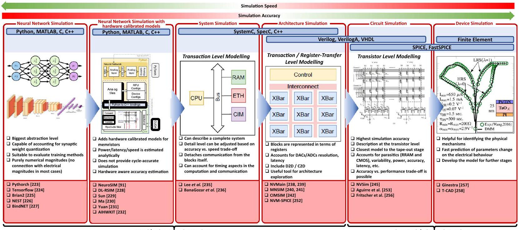
الرؤية ومعالجة اللغة الطبيعية. كلاهما مكتبات بايثون محسّنة للغاية لاستغلال وحدات معالجة الرسومات ووحدات المعالجة المركزية لمهام التعلم العميق. تتيح هذه المحاكيات تدريب وتطوير هياكل الشبكات العصبية المعقدة (مثل هياكل الشبكات العصبية التلافيفية مثل VGG و AlexNET أو الشبكات العصبية المتكررة – RNN). على الرغم من شعبيتها الكبيرة، فإن هذه المحاكيات لا توفر أي رابط على الإطلاق مع الأجهزة الميمريستيفية أو CMOS، حيث أن الكميات المعنية غير بعدية وتمثل الاتصالات المشبكية بقيم عددية غير مقيدة بشكل صارم.
حل شائع للتغلب جزئيًا على هذه القيود، خاصة في حالة الشبكات العصبية النابضة (نوع معين من الشبكات العصبية الاصطناعية حيث يتم ترميز متجه الإدخال من حيث معدل الإطلاق أو التوقيت بدلاً من سعات الجهد)، كان استخدام المحاكيات الموجهة نحو البيولوجيا. من بينها، براين2. يمكن تنفيذ الكود المكتوب بلغة بايثون بسهولة على وحدة المعالجة المركزية أو وحدة معالجة الرسوميات مع تنفيذ مجموعة واسعة من الخلايا العصبية وطرق ترميز المدخلات والعديد من طرق التعلم مثل البلاستيكية المعتمدة على توقيت النبضات (STDP). مع أخذ كل هذا في الاعتبار واعتبار أن تركيز Brian2 هو على المرونة وسهولة الاستخدام بدلاً من الأداء، فإنه يدعم فقط المحاكاة التي تعمل على جهاز واحد. محاكي بديل يحتفظ بكل هذه الميزات بينما يوفر أيضًا دعمًا للمحاكاة الموزعة عبر مجموعة هو محاكي NEST. بديل آخر لـ Brian2 قادر على تقديم أداء أفضل بتكلفة انخفاض الدقة للنموذج البيولوجي الحقيقي هو محاكي BindsNET. مكتبة بايثون مبنية على قمة باي تورش بصرف النظر عن دعم تشغيل وحدة المعالجة المركزية / وحدة معالجة الرسوميات وأخذ في الاعتبار مجموعة واسعة من الخلايا العصبية وطرق ترميز المدخلات والعديد من طرق التعلم (مثل STDP)، يمكن استخدام BindNET على منصات الأجهزة المتعددة مثل: الدوائر المتكاملة الخاصة بالتطبيقات (ASIC) ، والدوائر القابلة للبرمجة على الحقل (FPGA) ، ومعالجة الإشارات الرقمية (DSP) أو المنصات المعتمدة على معمارية RISC المتقدمة (ARM).
نهج آخر مثير للاهتمام تم اقتراحه في الأدبيات هو إضافة وحدات مخصصة إلى نماذج الشبكات العصبية في TensorFlow أو PyTorch، والتي تكون مسؤولة عن التقاط عدم المثالية الناتجة عن استخدام الميمريستور. يمكن اعتبار هذا النهج فئة فرعية ضمن هذه المجموعة، التي تأخذ في الاعتبار نماذج الأجهزة المعايرة. ضمن هذه المجموعة، وجدنا على سبيل المثال محاكي DLRSIM، الذي اقترحه لين وآخرون. ، الذي يحاكي معدلات الخطأ في كل عملية جمع للمنتجات في المسرعات المعتمدة على الميمريستور من الخارج، ويحقن الأخطاء في نماذج الشبكات العصبية المعتمدة على TensorFlow المستهدفة. كانت نفس الفلسفة
اعتمدت من قبل صن وآخرون. ، مع التركيز بشكل خاص على تأثير الطبيعة غير الخطية والمكمّلة لتحديث وزن المشبك. نظرًا لأن كلا الحالتين تعتبران TensorFlow لتنفيذ المحاكي، فإنهما تقدمان دعمًا لتحويل الشبكات العصبية العميقة المدربة مسبقًا، واستدلال معزز بواسطة وحدة معالجة الرسوميات، ورسم الخرائط للمعلمات. ومع ذلك، فإن الجانب السلبي هو أن هذه قطع من البرمجيات مغلقة إلى حد ما، وهو ما تم حله جزئيًا بواسطة ما وآخرون. ويوان وآخرون باستخدام PyTorch بدلاً من TensorFlow، مع التركيز في هذه الحالة على تأثيرات تقليم الوزن والتكميم. أيضًا، مجموعة تسريع الأجهزة التناظرية من IBM التي اقترحتها IBM يمكن أن يتم إدراجها ضمن هذه المجموعة. هذا الإطار يحاكي الشبكات العصبية باستخدام نماذج أجهزة تم معايرتها مع الأجهزة وعيوب الدوائر. ومع ذلك، فإنه يوفر فقط تقديرات الدقة باستخدام نماذج ضوضاء تم معايرتها مع الأجهزة ويفتقر إلى المحاكاة الدقيقة للدورات الزمنية أو الطاقة. مثال أخير (على الرغم من وجود حالات أخرى) هو NeuroSim. . يمكن لهذا المحاكي أن يأخذ في الاعتبار خصائص نوع الذاكرة، ومعلمات الأجهزة غير المثالية، وعقد تكنولوجيا الترانزستور، وتوبولوجيا الشبكة، وحجم المصفوفة، ومجموعة بيانات التدريب من خلال رسم نماذج الشبكات العصبية الاصطناعية على موارد البلاط، وجدولة تنفيذ عبء العمل الكامل، والذي من خلاله يقدم مقاييس دقة مدركة للأجهزة. على الرغم من أنه يقدم أيضًا معلمات نظام أخرى مثل المساحة، والكمون، واستهلاك الطاقة الديناميكي، إلا أن هذه المعلمات يتم الحصول عليها من خلال تقديرات تحليلية وليس من خلال محاكاة دقيقة للدورات. بشكل عام، تعتبر هذه الأدوات مفيدة جدًا لتقدير مبكر لدقة التعلم في وقت التشغيل.

محاكاة على مستوى النظام

أعلى مستوى تجريدي يحتفظ ببعض درجة من الاتصال مع تنفيذ الأجهزة لشبكة الأعصاب هو محاكاة مستوى النظام، والتي يمكن اعتبارها حالة خاصة من نمذجة مستوى المعاملات (TLM). في TLM، يتم فصل تفاصيل الاتصال بين مكونات الحساب عن الآليات الفيزيائية التي تحكم تلك المكونات. يتم نمذجة الاتصال بواسطة قنوات، بينما تحدث طلبات المعاملات من خلال استدعاء وظائف واجهة نماذج هذه القنوات. يتم إخفاء التفاصيل غير الضرورية للاتصال والحساب في TLM وقد تتم إضافتها لاحقًا (انظر القسم الفرعي التالي محاكاة مستوى العمارة). يمكن استغلال ذلك بشكل كبير عند استخدام TLM لأساليب من أعلى إلى أسفل تبدأ التصميم من سلوك النظام الذي يمثل وظيفة التصميم؛ ثم، يتم توليد بنية نظام مبسطة من السلوك، وتصل تدريجياً إلى
الجدول 4 | ملخص للأطر المحاكاة المبلغ عنها لدراسة الشبكات العصبية الصلبة الميمريستيفية
إطار المحاكاة سنة منصة تدريب نوع المحاكاة المصدر المفتوح نوع الشبكة العصبية الاصطناعية تطوير متوافق طاقة دقة قوة الكمون التغير CMOS وحدة معالجة الرسوميات
تينسورفلو 2015 بايثون نعم شبكة عصبية نعم MLP، CNN لا تطوير. لا نعم لا لا نعم لا لا لا نعم
بايتورتش 2017 بايثون نعم شبكة عصبية نعم MLP، CNN لا تطوير. لا نعم لا لا نعم لا لا لا نعم
عصبون 2006 بايثون نعم شبكة عصبية نعم SNN لا تطوير. لا نعم لا لا نعم لا لا لا نعم
براين2 2019 بايثون نعم شبكة عصبية نعم SNN لا تطوير. لا نعم لا لا نعم لا لا لا نعم
عش 2007 بايثون نعم شبكة عصبية نعم SNN لا تطوير. لا نعم لا لا نعم لا لا لا نعم
بايندزنت 2018 بايثون نعم شبكة عصبية نعم SNN لا تطوير. لا نعم لا لا نعم لا لا لا نعم
ميمتورش ٢٠٢٠ بايثون، C++، كودا لا شبكة نيورلا نعم سي إن إن ذاكرة الوصول العشوائي المقاومة لا نعم لا لا نعم لا لا لا نعم
NVMain 2015 C++ لا العمارة نعم ذاكرة ذاكرة الوصول العشوائي المقاومة نعم لا نعم نعم لا لا لا لا لا
بوما 2019 C++ لا العمارة لا MLP، CNN ذاكرة الوصول العشوائي المقاومة نعم نعم نعم نعم لا لا لا نعم نعم
رابيد إن إن 2018 C++ لا العمارة لا MLP، CNN ذاكرة الوصول العشوائي المقاومة نعم نعم نعم نعم نعم لا لا نعم لا
دي إل-آر إس آي إم 2018 بايثون لا العمارة لا MLP، CNN ذاكرة الوصول العشوائي المقاومة لا نعم لا لا نعم لا لا لا نعم
طبقة الأنابيب 2017 C++ نعم العمارة لا سي إن إن ذاكرة الوصول العشوائي المقاومة نعم نعم نعم لا لا لا لا لا
صغير ولكن دقيق 2019 ماتلاب لا العمارة نعم سي إن إن، ريس نت ذاكرة الوصول العشوائي المقاومة نعم نعم نعم لا لا لا لا لا لا
يوان وآخرون 2019 سي++، ماتلاب نعم العمارة نعم لا توجد بيانات ذاكرة الوصول العشوائي المقاومة لا نعم نعم لا لا لا لا لا نعم
سون وآخرون 2019 بايثون نعم العمارة لا MLP PCM، STT-RAM، ReRAM، SRAM، FeFET نعم نعم نعم لا نعم لا لا لا لا
أ. تشين 2013 ماتلاب لا دائرة نعم MLP ذاكرة الوصول العشوائي المقاومة لا لا نعم لا نعم نعم لا لا لا
CIM-SIM 2019 SystemC (C++) لا العمارة نعم SLP ذاكرة الوصول العشوائي المقاومة لا لا لا لا لا لا لا لا لا
MNSIM 2018 بايثون لا العمارة نعم سي إن إن ذاكرة الوصول العشوائي المقاومة نعم لا نعم نعم نعم لا لا لا نعم
NVSIM 2012 C++ لا دائري نعم ذاكرة PCM، STT-RAM، ReRAM، فلاش نعم لا نعم نعم لا لا لا لا لا
كروس سيم 2017 بايثون لا توجد بيانات دائري نعم لا توجد بيانات PCM، ReRAM، فلاش لا نعم لا لا نعم نعم لا لا نعم
نيرو سيم ٢٠٢٢ بايثون، سي++ نعم دائري نعم MLP، CNN PCM، STT-RAM، ReRAM، SRAM، FeFET نعم نعم نعم لا نعم لا لا لا نعم
NVM-SPICE 2012 غير محدد لا دائري لا SLP ذاكرة الوصول العشوائي المقاومة نعم لا نعم نعم نعم لا لا نعم لا
مجموعة تسريع الأجهزة التناظرية من IBM ٢٠٢١ بايثون، C++، كودا نعم شبكة عصبية نعم MLP، CNN، LSTM PCM لا نعم لا لا نعم لا لا لا نعم
فريتشر وآخرون 2019 مختلط (VHDL، Verilog، SPICE) لا دائري لا MLP PCM، STT-RAM، ReRAM، SRAM، FeFET نعم نعم نعم نعم نعم نعم نعم نعم نعم
أغيري وآخرون ٢٠٢٠ مختلط (بايثون، ماتلاب، سبايس) لا دائري لا MLP PCM، STT-RAM، ReRAM، SRAM، FeFET نعم نعم نعم نعم نعم نعم نعم نعم نعم
الشكل 16 | تفاصيل المراحل المختلفة لنمذجة مستوى المعاملات، مع إضافة الشبكة العصبية والمحاكاة على مستوى الترانزستور (الدائرة). يتم ترتيب أساليب النمذجة بناءً على مدى دقة (غير مؤقت، تقريبي، دقيق للدورات) التقاط توقيت جوانب الحساب والتواصل. ثم تتوسع نماذج مستوى المعاملات من إلى مع كونها نماذج المواصفات (التي تعتبر الاتصال والحساب غير محددين زمنياً) و G نماذج التنفيذ (التي تأخذ في الاعتبار التوقيت الدقيق لكل من الحساب والاتصال). مع اقترابنا من B، يمكن اعتبار النموذج محاكاة على مستوى النظام، بينما إذا اقترب من G، يُعتبر محاكاة على مستوى العمارة. خارج هذه المجموعة، نجد تلك النماذج التي تم محاكاتها في بايثون أو أدوات مشابهة والتي تركز على طوبولوجيا الشبكة (A) والنماذج الدائرية التي تجسد نماذج التنفيذ (G) على مستوى الترانزستور أو مستوى نقل السجل.
نموذج التنفيذ من خلال إضافة تفاصيل التنفيذ. إن القدرة على تخصيص تفاصيل تمثيل الاتصالات ونوى الحساب هي التي تمكن من أداء عالي الإنتاجية (دائمًا على حساب تقليل الدقة والاتصال بالآليات الفيزيائية التي تحكم استجابة الميمريستور). على الرغم من عدم الاقتصار على ذلك، تشمل منصات البرمجة التقليدية لمحاكاة المستوى النظامي / نمذجة مستوى المعاملات SystemC. و SpecC .
تشمل أمثلة على هذا المستوى من تجريد المحاكاة العمل الذي قام به لي وآخرون. ، الذي قدم محاكي نظام دقيق لدورة الزمن لنمذجة الشبكات العصبية النابضة المنفذة على الأجهزة. تتبع هذه الشبكات هيكلًا هرميًا يعتبر نظام الحوسبة في الذاكرة كترابط بين النوى العصبية أو البلاطات، وكل من هذه النوى تم إنشاؤها في النهاية من خلال التجميع المشترك لوحدات التقاطع. يوفر تمثيل التقاطع القدرة على محاكاة التأثيرات غير المثالية للأجهزة الفعلية من نوع RRAM، والتي تشمل التأثيرات غير الخطية لـ RRAM مثل الأعطال الثابتة (SAFs)، وتنوع الكتابة، وضوضاء التلغراف العشوائية (RTN). من الجدير بالذكر أنه لتوصيل البلاطات بكفاءة، يتم استخدام شبكة مخصصة على الرقاقة (NoC)، والتي، جنبًا إلى جنب مع وصف وحدة التقاطع، تسمح بمرونة عالية وقابلية للتكوين.
مقارنةً بالمرجع 235، محاكي BanaGozar وآخرون. تركز على تكامل أنظمة الحوسبة العصبية. وبالتالي، قام المؤلفون بتنفيذ مجموعة تعليمات دقيقة للتحكم في المكونات التناظرية والرقمية للنظام. بشكل عام، يتبع المحاكي هيكلًا هرميًا مشابهًا لما هو موجود في المرجع 235 من خلال تنفيذ الحوسبة في الذاكرة (CIM) في وحدات. تتكون هذه الوحدات من ميمريستيف.
ممر الذاكرة، المحولات التناظرية/الرقمية، معدلات الإدخال الرقمية ومراحل العينة والاحتفاظ. علاوة على ذلك، يحتوي كل بلاط على وحدة تحكم مخصصة تنظم المكونات المسؤولة عن دفع الحساب.

محاكاة على مستوى العمارة

نظرًا لقدرات التخصيص الخاصة بها، يمكن تقسيم TLM إلى فئات مختلفة كما أشار غاي وآخرون. (انظر الشكل 16). نماذج المواصفات (B) هي تلك التي تحتوي على أدنى درجة من التفاصيل وتقع أقرب إلى نماذج الشبكات العصبية (A) الموصوفة سابقًا. في الزاوية المقابلة، نماذج التنفيذ (G) هي الخطوة التي تسبق مباشرة نماذج الدوائر. تم تصميمه على مستوى الترانزستور. مع اقتراب TLM من مرحلة نماذج التنفيذ، يُشار إليها أيضًا كنماذج مستوى نقل السجل (RTL) وتجسد ما يُطلق عليه أحيانًا محاكاة مستوى العمارة. بعبارة أخرى، يمكن اعتبار محاكاة مستوى العمارة كنوع فرعي من TLM بمزيد من التفاصيل المتعلقة بواجهات الاتصال والحساب. أيضًا، مع زيادة مستوى التفاصيل، ينتقل لغة البرمجة من SpecC وsystemC (المستخدمة في المحاكاة على مستوى النظام) إلى لغات وصف الأجهزة، مثل Verilog وVerilog-A أو HDL، وحتى مزيج من لغات البرمجة مثل C++ وCUDA وMATLAB وPython لمحاكاة سلوك الأجهزة الميمريستيفية أثناء الاستدلال.
محاكيات الذاكرة غير المتطايرة الناشئة NVMain (وخليفتها، NVMain ) تم اقتراحها من قبل بوريمبا وآخرين، كمثال على محاكيات الذاكرة الرئيسية على مستوى العمارة، والتي تتميز بمرونة عالية وسهولة في الاستخدام. على الرغم من أن NVMain 2.0 يسمح بتقدير مقاييس استهلاك الطاقة بناءً على نتائج المحاكيات على مستوى الدائرة، إلا أن له قيودًا. نظرًا لأنه يركز على المحاكيات الموجهة للذاكرة للهياكل غير المتطايرة الناشئة، فإنه لا يدعم تضمين الدوائر المحيطية التي ستكون ضرورية لنمذجة هياكل الحوسبة في الذاكرة. للتغلب على هذا التحدي، قام شيا وآخرون. قدمت MNSIM وقدم زو وآخرون الخلف MNSIM . يستخدم المحاكي نموذجًا سلوكيًا لتقدير أسوأ حالة ومتوسط الدقة، مما يحسن بشكل كبير أداء المحاكاة. نظرًا لأن الأجهزة الميمريستيفية تظهر خصائص I-V غير الخطية، يقوم النموذج السلوكي بتقريب الخصائص الفيزيائية باستخدام دالة خطية لتقليل الجهد الحاسوبي. ونتيجة لذلك، يتم زيادة الأداء. يقترح هيكلًا هرميًا لمسرعات الحوسبة العصبية المستندة إلى الميمريستور، مع واجهات للتخصيص. تشمل المحاكيات على مستوى المعمارية الأخرى المقترحة في الأدبيات والتي تتبع نهجًا مشابهًا CIM-SIM. و XB-SIM .
التعمق في التفاصيل، محاكي MNEMOSENE يضيف قدرات دقيقة للدورات إلى محاكيات مستوى البلاط من خلال تنفيذ التعليمات في الذاكرة (في سياق الشكل 16، يمكن تفسير ذلك كنموذج تنفيذ، كما هو موضح بالكرة G). كما يتيح للمستخدم تتبع جميع إشارات التحكم ومحتوى المبدلات/السجلات، وبفضل البرمجة المودولارية للمحاكي، يمكن للمستخدم بسهولة استكشاف تقنيات الميمريستور المختلفة، وتصميمات الدوائر، ونمذجة المبدلات الأكثر تقدمًا (على سبيل المثال، مع الأخذ في الاعتبار تباين القراءة/الكتابة). ثم، للمضي قدمًا نحو المسار نحو أكثر محاكيات الشبكات العصبية الميمريستية دقة، تم اقتراح PUMAsim من قبل أنكيت وآخرين. تستخدم Verilog HDL لنمذجة البلاط والنوى على مستوى نقل السجل، مما يسمح لها بأن تُخَطَّط في عملية CMOS على السيليكون المعزول بحجم 45 نانومتر لتقدير المساحة. حتى هذه النقطة، وبغض النظر عن مستوى التفاصيل (مستوى النظام أو مستوى العمارة)، يمكن تأطير المحاكيات بين الحالات الموصوفة من العقد B-G في الشكل 16. الخطوة النهائية هي وصف كل من الكتل المكونة من حيث الأجهزة الكهربائية المطلوبة، أي، الترانزستورات والميمريستور.

محاكاة مستوى الدائرة

للتعامل مع الحوسبة المستوحاة من الأعصاب على مستوى الدائرة، قام دونغ وآخرون. اقترح NVSim الذي يمثل محاكيًا للتقنيات الناشئة
ذاكرات غير متطايرة مثل STT-RAM وPCRAM وهياكل ReRAM. وهذا يسمح: i) بتقدير وقت الوصول، طاقة الوصول ومساحة السيليكون، ii) استكشاف مساحة التصميم، و iii) تحسين الشريحة لمقياس تصميم محدد واحد. ومع ذلك، وبالمثل لـ NVMain تركز NVSim بشكل أساسي على نمذجة هياكل الذاكرة غير المتطايرة بدلاً من وحدات الحوسبة في الذاكرة. وقد تم اقتراح بدائل للتغلب على هذه القيود، مثل المحاكي الذي طوره سونغ وآخرون. لتقييم بنية PipeLayer الخاصة بهم، التي تأخذ في الاعتبار التصاميم عالية التوازي بناءً على مفهوم دقة التوازي وتكرار الوزن. يعتمد هذا المحاكي على NVSim ويوفر وظيفة عالية المستوى لتلبية متطلبات محاكاة الحاسوب في الذاكرة. وهذا هو الحال أيضًا مع RAPIDNN. الذي يعتمد على محاكاة H-SPICE وNvsim لتقييم استهلاك الطاقة والأداء. تم تغطية بديل آخر لمحاكاة مستوى الدائرة بشكل كبير في الأدبيات عند السعي لمحاكاة هياكل الكروس بار البسيطة من نوع 1R. تم الإبلاغ عن هذه المنهجية في البداية بواسطة تشين. , ثم تم استغلاله بشكل أكبر في المراجع 249-251، يصف سلوك الهيكل الكهربائي للهيكل المتقاطع من خلال تمثيله الرياضي المرتبط، كنظام من المعادلات المترابطة.
على الرغم من أن كلا الطريقتين الموصوفتين سابقًا يمكن أن تتعامل مع تحدي محاكاة الدوائر على مستوى الأجهزة لمكونات الميمريستور (الثانية في الواقع فقط للإشارات الثابتة DC) إلا أنهما تفشلان في أخذ الهياكل الهجينة CMOS-memristor في الاعتبار. في هذا السيناريو، من الضروري النظر في المحاكيات القادرة على التعامل مع نماذج CMOS القياسية في الصناعة، ويفضل أن تكون على مستوى SPICE وإذا لم يكن، على الأقل على مستوى RTL. هذه هي حالة العمل الذي قام به فيي وآخرون. , على الرغم من أن أداة المحاكاة المقترحة لم يتم تقييمها لشبكات الأعصاب الهجينة CMOS-memristor. في هذا الصدد، في عملنا السابق اقترحنا روتين محاكاة يقوم، من مجموعة من المعلمات المعطاة (مثل حجم الشبكة، الخصائص الكهربائية للميمريستور والعيوب غير المثالية، التوصيلات)، بإنشاء شبكة عصبية هجينة CMOS-memristive مدربة مسبقًا موصوفة كقائمة شبكية SPICE (أي، ملف نصي يصف الدائرة). تم استخدام هذه الإجراء بنجاح لتقييم الدقة، واستهلاك الطاقة، والكمون، وغيرها من معايير الأداء لشبكات الأعصاب المعتمدة على الأجهزة أثناء الاستدلال . كما يسمح بدراسة عملية تحديث الوزن بالتفصيل وتخفيف الأخطاء الثابتة . لتسريع عملية المحاكاة، نعتمد في هذا التنفيذ على محاكي FastSPICE من مجموعة تصميم Synopsys، على الرغم من أنه متوافق تمامًا مع H-SPICE القياسية. تم اتباع مسار مشابه من قبل فريتشر وآخرون. ولكن مع الأخذ في الاعتبار مجموعة تصميم Cadence. خاصية مثيرة للاهتمام هي أن البيئة تجمع بين محاكي الدوائر التناظرية Cadence Spectre مع Cadence Incisive، وهو محاكي على مستوى النظام، لنمذجة نظام كامل من الجهاز إلى مستوى النظام بطريقة شاملة جدًا. كتعليق نهائي، لتغطية الشكل 15 بالكامل، فإن المحاكيات على مستوى الجهاز مثل Ginestra أو T-CAD مخصصة لمحاكاة قائمة على الفيزياء على المستوى الذري لجهاز واحد، ويتم استخدام مخرجاتها بعد ذلك لمزيد من ضبط النماذج المدمجة المستخدمة في محاكاة SPICE.
سلسلة أدوات تصميم البرمجيات والأجهزة المشتركة تعني تحسين جميع المكونات المعنية في تنفيذ الأجهزة لشبكات الأعصاب، بما في ذلك أداء جهاز الميمريستور، وكتل الدوائر، وهيكلية العمارة والتواصل بين الكتل. هناك نقص في أداة تجارية فعالة لتصميم البرمجيات والأجهزة المشتركة، حيث إن المحاكيات على مستوى الجهاز لا تأخذ في الاعتبار مستوى العمارة والتواصل على الشريحة، بينما تفتقر المحاكيات على مستوى العمارة إلى اعتبار خصائص الجهاز الواقعية .
بالإضافة إلى اعتبارات التصميم على مستوى الأجهزة، يمكن أن تؤثر المعلمات المتعلقة بالبرمجيات المختارة لشبكة الأعصاب أيضًا على أداء الأجهزة. تشمل هذه المعلمات المتعلقة بالبرمجيات عدد الخلايا العصبية والطبقات في الشبكة، وأحجام نوى الالتفاف، ودوال التنشيط، وما إلى ذلك. على سبيل المثال،
يمكن تخفيف العيوب غير المثالية المتعلقة بالميمريستور من خلال تحسين المعلمات المتعلقة بالبرمجيات لشبكة الأعصاب . تشير المرجعية 260 إلى أنه يمكن تحسين معلمات تصميم شبكة الأعصاب لتقليل آثار تقلبات التوصيل والانجراف في الميمريستور دون المساس بدقة الأداء. لذلك، من المهم تحسين كل من معلمات البرمجيات والأجهزة معًا لتحقيق دقة أداء عالية وكفاءة في الأجهزة لمكونات الشبكة العصبية المعتمدة على الميمريستور وتخفيف العيوب غير المثالية للجهاز.
يكمن هذا التحسين في مجال بحث بنية الشبكات العصبية المدركة للأجهزة، والذي يقوم بتحسين معلمات تصميم شبكة الأعصاب مع الأخذ في الاعتبار ردود الفعل من الأجهزة ، أو في بعض الحالات، يبحث عن معلمات الأجهزة المثلى . على سبيل المثال، يمكن البحث عن حجم الهيكل المتقاطع المثالي ، دقة ADC/DAC، ودقة الجهاز جنبًا إلى جنب مع المعلمات المتعلقة بالبرمجيات لشبكة الأعصاب. تأخذ المراجع 263،264 في الاعتبار تقلبات جهاز الميمريستور عند البحث عن معلمات شبكة الأعصاب المتعلقة بالبرمجيات المثلى. يمكن إجراء بحث عن معلمات التصميم باستخدام التعلم المعزز ، أو الخوارزميات التطورية ، أو الطرق التفاضلية . يعد بحث بنية الشبكات العصبية المدركة للأجهزة نهجًا واعدًا لأتمتة تصميم البرمجيات والأجهزة المشتركة لشبكات الأعصاب المعتمدة على الميمريستور.

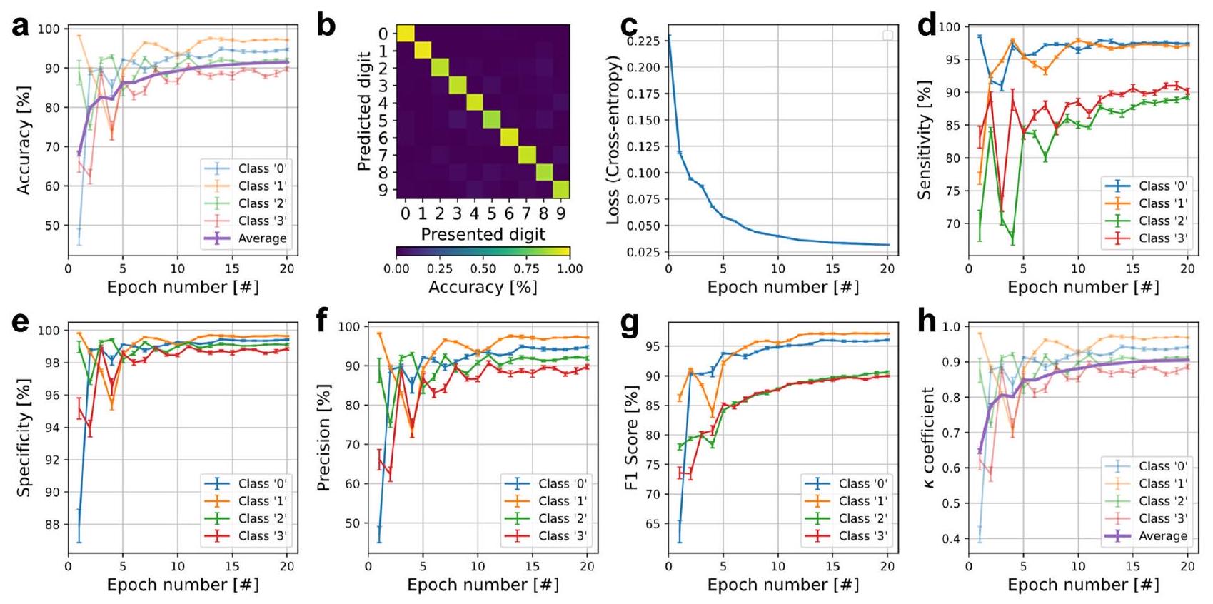
مثال على تحليل ANN الميمريستيف

لتقييم جدوى جهاز ميمريستور (تم تنفيذه في مصفوفات متقاطعة) لتصنيف الصور، قمنا بتطوير إجراء لإنشاء ومحاكاة بيرسيبترون ذو طبقة واحدة (SLP) . هذا النوع من الشبكات العصبية أبسط من تلك التي تم اعتبارها في شبكات ANN الميمريستيف الأكثر تعقيدًا، مثل بيرسيبترون متعدد الطبقات (MLP) ، والشبكات العصبية الالتفافية (CNNs) ، والشبكات العصبية النابضة (SNNs) ، من بين آخرين (انظر الجدول 5). ومع ذلك، فإنه يسمح بدراسة وتوضيح قيود شبكات ANN الناتجة عن التأثيرات الطفيلية والعيوب غير المثالية التي تحدث في الطبقات المشبكية المنفذة بمصفوفات متقاطعة من أجهزة الميمريستور. تشمل هذه التأثيرات تأثير المقاومة غير القابلة للتجاهل للتوصيلات الخطية، نافذة المقاومة المحدودة ( )، نسبة الإشارة إلى الضوضاء (SNR)، تباين الوزن المشبكي، وكمون الاستدلال، من بين أمور أخرى. الإجراءات المقدمة هنا صالحة بغض النظر عن خلية الذاكرة المعنية (1T1R أو 1R). يمكن توسيع الإجراء المقدم بسهولة نسبيًا لـ MLPs؛ في هذه الحالة، يتم تكرار مرحلة توليد الدائرة بقدر ما تحتويه MLP من طبقات.
لأغراض البساطة، سيتم اعتبار التعلم الخاضع للإشراف خارج الموقع هنا. بمجرد التدريب، يتم تحويل الأوزان المشبكية المحسوبة بواسطة هذا SLP القائم على البرمجيات إلى قيم توصيل يتم تنفيذها بعد ذلك باستخدام الميمريستور (أي، يتم برمجة توصيل كل ميمريستور إلى القيم المحسوبة بواسطة البرمجيات). يتم اعتبار التعرف على الأنماط من مجموعة بيانات MNIST كمعيار. يتم تلخيص سير العمل في الرسم البياني الموضح في الشكل التكميلية 9. يمكن تقسيم العملية العامة إلى جزئين: الأول يتضمن مجموعة من الروتينات الفرعية في MATLAB لإنشاء، وتدريب، وكتابة قائمة SPICE لشبكة SLP، بينما يتعلق الجزء الثاني بمحاكاة SPICE للدائرة المقترحة خلال مرحلة التصنيف.

ترجمة الأوزان المشبكية من ANN القائم على البرمجيات إلى قيم توصيل

هناك طريقتان محتملتان لضبط كل من الميمريستورات الموضوعة في الهياكل المتقاطعة إلى قيم توصيلها المقابلة من و المصفوفات. واحدة هي محاكاة مرحلة البرمجة، حيث يتم تحقيق التوصيل المطلوب في كل جهاز من خلال تطبيق سلسلة من النبضات ذات السعة والعرض المتحكم فيه مع مراقبة الزيادة التدريجية في توصيل الجهاز حتى الوصول إلى هدف. ومع ذلك، فإن هذه العملية تتطلب موارد محاكاة كبيرة خاصة للشبكات الكبيرة. إمكانية أخرى هي استخدام نموذج مدمج للميمريستور وتقدير قيمة المتغير الحالى
الجدول 5 | مقارنة الدقة التي تم الحصول عليها مع أنواع مختلفة من الشبكات العصبية المعتمدة على الميمريستور وخوارزميات التعلم، سواء من المحاكاة أو من الأساليب التجريبية
نوع الشبكة العصبية خوارزمية التعلم قاعدة البيانات الحجم التدريب الدقة المنصة المرجع.
(محاكاة) (تجريبية)
بيرسيبترون ذو طبقة واحدة (SLP) الانتشار العكسي (تدرج مترافق مقاس) MNIST ( بكسل.) طبقة واحدة ( ) خارج الموقع ~91% محاكاة SPICE نموذج QMM 253
قاعدة تحديث مانهاتن نمط مخصص طبقة واحدة ( ) في الموقع ND تجريبي ( ) 105
وجه ييل طبقة واحدة ( ) في الموقع تجريبي ( ) 194
بيرسيبترون متعدد الطبقات (MLP) الانتشار العكسي (تدرج عشوائي متناقص) MNIST ( ) طبقتان ( ) في الموقع تجريبي ( ) 54
الانتشار العكسي (تدرج مترافق مقاس) MNIST ( بكسل.) k طبقات ( ) خارج الموقع محاكاة SPICE نموذج QMM 253
الانتشار العكسي MNIST (14 ) طبقتان ( ) خارج الموقع ~92% ~82.3% برمجيات/ تجريبي ( ) 196
MNIST (22 ) طبقتان ( ) في الموقع ~83% ~81% برمجيات/ تجريبي (PCM) 267
MNIST (28 ) طبقتان ( ) خارج الموقع ~97% برمجيات (بايثون) 288
الانتشار العكسي Sign MNIST ( ) طبقة واحدة ( ) في الموقع ~94.5% برمجيات (MATLAB) 289
شبكة عصبية تلافيفية (CNN) الانتشار العكسي MNIST ( ) طبقة مزدوجة (الطبقة الأولى: تلافيفية، الطبقة الثانية: كاملة التوصيل) في الموقع حوالي 94% برمجيات ٢٦٨
شبكة الأعصاب النابضة (SNN) المرونة المعتمدة على توقيت النبضات (غير خاضعة للإشراف) MNIST ( ) طبقة مزدوجة ( ) في الموقع ~93.5% البرمجيات (C++ Xnet) ٢٦٩
لاحظ أنه في جميع الحالات يتم تنفيذ الطبقات المشبكية باستخدام CPAs وتتم المحاكاة دون أخذ في الاعتبار الشوائب الخطية أو نماذج الميمريستور الواقعية. نظرًا لأن CPA هو عنصر أساسي في هذه الشبكات العصبية المعقدة، فإن المحاكاة الواقعية باستخدام SPICE لـ CPA لا تزال مطلوبة.
في معادلة الذاكرة التي تؤدي إلى التوصيل المستهدف. بالنسبة لحالة نموذج الميمود (QMM) شبه الثابت المعتبر في المراجع 250 و 253، يتم ذلك عن طريق ضبط المعامل التحكم. الذي يتراوح بين 0 (HRS) و 1 (LRS). القيمة المطلوبة لـ يتم الحصول عليه عن طريق حل المعادلة 14:
لـ ، مع ، كون كل من عناصر و في المعادلة هو سعة تيار الدايود، ثابت مناسب، و مقاومة متسلسلة. المعادلة 14 هي حل لدياود مع مقاومة متسلسلة و هي دالة لامبرت. و هي القيم الدنيا والقصوى لسعة التيار، على التوالي. هو القيمة المطلقة للتحيز المطبق و دالة الإشارة. كـ الزيادات في المعادلة 14، تتغير منحنى شكلها من أسّي إلى خطي من خلال مجموعة مستمرة من الحالات، كما لوحظ تجريبيًا لهذا النوع من الأجهزة. . يتم حل هذه المعادلة لكل من الميمريستور في المصفوفة الإيجابية والسلبية، كما هو موضح في الخوارزمية التكميلية 4. ونتيجة لذلك، يتم الحصول على مصفوفتين مختلفتين ( و ) يتم إنتاجها. لاحظ أنه بالنسبة لنماذج الميمريستيف الأخرى، سيتم حساب متغير الحالة وفقًا لمعادلة مختلفة (على سبيل المثال في نموذج ستانفورد ).
المقاومة غير القابلة للتجاهل للخطوط المعدنية التي تربط الأقطاب العليا والسفلى للذاكرات المدمجة في هيكل متقاطع تنتج انخفاضًا في الجهد (IR) على طولها مما يقلل من الجهد المقدم للذاكرات. تتفاقم هذه الظاهرة بالنسبة للذاكرات الموجودة بعيدًا عن المدخلات (أطراف صفوف الهيكل المتقاطع) والمخرجات (أطراف أعمدة الهيكل المتقاطع)، حيث أن خطوط التوصيل المطلوبة للوصول إلى مثل هذه الأجهزة تصبح أطول بشكل متزايد. هناك قبول واسع لـ يتكون التصميم البديل لتقليل هذه المشكلة من تقسيم العوارض العرضية الكبيرة إلى عوارض أصغر (الشكل التوضيحي التكميلي 9ب)، حيث أن حجمها المنخفض يحسن هامش القراءة الخاص بها (أي الجزء من الجهد المطبق في المدخلات الذي هو
تم تسليمها فعليًا إلى الميمريستورز). يتم الإشارة إلى عدد الأقسام بـ NP، ويعتمد الحجم الموصى به لكل قسم على نسبة التوصيلية بين الميمريستورز ومقاومة الأسلاك المعدنية. توضح الشكل التوضيحي 10 المبسط للعبور المقسم والاتصالات المطلوبة لتحقيق VMM الكامل. من خلال تفجير قابلية التكامل للعبور مع دوائر CMOS، يمكن وضع الاتصالات الرأسية المستخدمة لربط مخرجات أقسام العبور الرأسية تحت الهيكل المقسم (بالإضافة إلى الإلكترونيات الحسية التناظرية) مما يسمح للعبور المقسم بالحفاظ على استهلاك مساحة مشابه للحالة الأصلية غير المقسمة. . يتم تأريض التوصيلات الرأسية من خلال دائرة الاستشعار (أي TIA) لامتصاص التيارات داخل نفس السلك العمودي. لتحقيق هذه البنية المقسمة، كلا من و تُقسم المصفوفات إلى أجزاء أصغر (كما هو موضح في الجزء العلوي من الشكل التكميلية 9b). يتم تعيين كل من هذه الأقسام إلى تقاطع ميمريستور مختلف. على سبيل المثال، يتم تعيين تلك المصفوفات الأربعة المختلفة إلى الأربعة تقاطعات المختلفة في الشكل التكميلية 10.

إنشاء تمثيل دائرة الشبكة العصبية الميمريستيفية

في الخطوة التالية، يتم استخدام البرنامج (MATLAB في هذا المثال) لكتابة (سطرًا بسطر) قائمة الشبكة SPICE التي تتوافق مع شبكة ANN المعتمدة على مصفوفة memristor، مع الأخذ في الاعتبار مخطط الاتصال (المصفوفات الإيجابية والسلبية، كل منها مقسم) والمنطق التحكم الضروري لتنفيذ مرحلة الاستدلال. يصف الشكل 17 مستويات التجريد المختلفة بدءًا من التمثيل الرياضي البحت لـ VMM (الشكل 17أ)، ثم إلى مخطط الكتلة الذي يتضمن الكميات الكهربائية (الفولتية، التوصيلات، المقاومات والتيارات، انظر الشكل 17ب)، ثم إلى مخطط الدائرة بدون تأثيرات جانبية (بما في ذلك في هذه المرحلة memristors والإلكترونيات التناظرية الضرورية، انظر الشكل 17ج)، للوصول أخيرًا إلى الدائرة التناظرية المعادلة التي تنفذ VMM بما في ذلك تأثيرات الدائرة الجانبية (الشكل 17د). في هذا المثال، نستخدم دالة fprintf() من MATLAB. ، واستخدمنا خلية ميمريستور تأخذ في الاعتبار جميع مقاومات الأسلاك وسعاتها. الكود المخصص المصنوع في MATLAB
الشكل 17 | تمثيلات مختلفة لعملية ضرب المصفوفات المتجهية النموذجية من طبقة مشبكية. (أ) عملية VMM الرياضية بدون وحدات. (ب) عملية VMM الرياضية التي تتضمن مقادير كهربائية. (ج) تمثيل الدائرة الكهربائية لعملية VMM التناظرية المعتمدة على مصفوفة الميمريستور. (د) تمثيل واقعي لمصفوفة الميمريستور مع الأخذ في الاعتبار مقاومة الخط. )
وسعات الخطوط المتداخلة (انظر الشكل المرفق الذي يظهر مخطط دائرة لخلية ميمريستيف في هيكل CPA مع الأخذ في الاعتبار مقاومة السلك الطفيلية والسعة المرتبطة). يتم التقاط جوانب مثل تباين الجهاز بواسطة نموذج الميمريستور المستخدم.
الشكل 18 | مخططات الاتصالات المستخدمة لتغذية CPA بنمط الإدخال.
أ) الاتصال من جانب واحد (SSC) و (ب) الاتصال من جانبين (DSC). في حالة SSC، يتم تطبيق المحفزات المدخلة فقط على مدخلات جانب واحد من CPA، بينما الجانب الآخر هو
ب
متصل بمقاومات عالية (أو يبقى غير متصل). في حالة DSC، يتم توصيل كلا طرفي خط الكلمات (الخطوط الأفقية في CPA) بنفس جهد الإدخال، مما يقلل من انخفاض الجهد على طول خطوط الكلمات.
يستقبل كمدخلات حجم المصفوفة ونظام التقسيم، ويحدد تلقائيًا عدد الميمريستورات التي يجب وضعها وكيفية توصيلها بمقاومات الخطوط المجاورة لتحقيق الهيكل الكهربائي المتقاطع. يستخدم هذا الكود المصدر حلقات for متداخلة تتكرر عبر عدد الصفوف والأعمدة، مما ينشئ الهيكل المتقاطع. أيضًا، يتم إضافة السعة الطفيلية بين الخطوط المتوازية المجاورة في نفس المستوى (أي بين الصفوف والأعمدة المجاورة)، وبين تقاطعات الخطوط العلوية والسفلية، وبين الخطوط السفلية والأرض. من خلال ذلك، يمكننا حساب تأخير الانتشار عبر الهيكل المتقاطع، المعروف أيضًا بالكمون (أي عندما يكون الهدف هو قياس الوقت المنقضي منذ تطبيق نمط في مدخلات SLP حتى يستقر الناتج). نتيجة لذلك، يتم توصيل كل ميمريستور في الهيكل المتقاطع بـ 4 مقاومات و 5 مكثفات، كما هو موضح في الشكل 17d. كمثال، الكود الناتج لـ SPICE لتمييز SLP تظهر صور البكسل في الخوارزمية التكميلية 5. لتجنب فقدان الجهد في أسلاك الشبكة المتقاطعة، استخدمنا مخطط الاتصال من الجانبين. على الرغم من زيادة تعقيد الدوائر المحيطية، فإن هذا المخطط يحسن توصيل الجهد إلى كل مشبك عصبي. عن طريق توصيل الطرفين لكل خط كلمة بنفس المحفزات المدخلة. الفرق بين الاتصال من الجانبين والاتصال من جانب واحد موضح في الشكل 18. في الممارسة العملية، عند تصميم الدوائر لتزويد جهد الإدخال للاتصال من الجانبين
مخطط الاتصال على شريحة، أي عدم تطابقات وتvariations في الفولتية (الشكل 18ب) يجب تجنبه. الفولتية يجب أن تكون من كلا جانبي العارضة متطابقة مع أسلاك الاتصال المصممة بعناية. أي اختلافات ناتجة عن اختلاف طول الأسلاك التي تربط صفوف العارضة بجهود الإمداد المدخلة يمكن أن تؤدي إلى انخفاضات غير مرغوب فيها في الجهد ومشاكل تتعلق بتيارات المسار الخفي.
يتم الحصول على المحفزات المدخلة عن طريق تغيير مقياس كل من الصور الرمادية غير الملفوفة البالغ عددها 10,000 من مجموعة بيانات اختبار MNIST، التي تم تخزينها سابقًا في متجه، بواسطة جهد كما هو موضح في الشكل 4ج. يتم اختيارها بحيث تمنع تغيير حالات الميمريستور أثناء محاكاة الاستدلال. بهذه الطريقة، يتم تقديم كل صورة اختبار إلى الشبكة المتقاطعة كمتجه خلال عملية الاستدلال. الجهود التناظرية في النطاق .
خلال مرحلة الاستدلال، يجب توصيل مدخلات الموزع المقسم بالجهود التي تمثل سطوع البكسلات، ويجب توصيل مخرجات الموزع بالدارات التناظرية المحيطية التي تتكون من مجمعات تم بناؤها باستخدام عدد قليل من المقاومات ومضخم تيار (انظر الشكل التوضيحي 9c على اليسار والشكل 19a). خلال مرحلة الكتابة، يحتاج الموزع المقسم إلى الاتصال بالدائرة المحيطية اللازمة لإنتاج المحفزات الكهربائية التي تبرمج موصلية الميمريستور إلى القيم.
الشكل 19 | تفاصيل الدوائر التحكمية المستخدمة لإجراءات الاستدلال/الكتابة المزدوجة. مخطط دائرة كامل لـ مصفوفة تقاطع 1T1R. تفاصيل المزامنات بما في ذلك مضخمات الإشارة المستخدمة لاكتشاف البرمجة الصحيحة لميمريستور معين. ج блок العنوان، وهو في الأساس عداد يقوم بتوجيه كل ميمريستور في الشبكة المتقاطعة بشكل متسلسل. المفككات الصفية والعمودية، المستخدمة
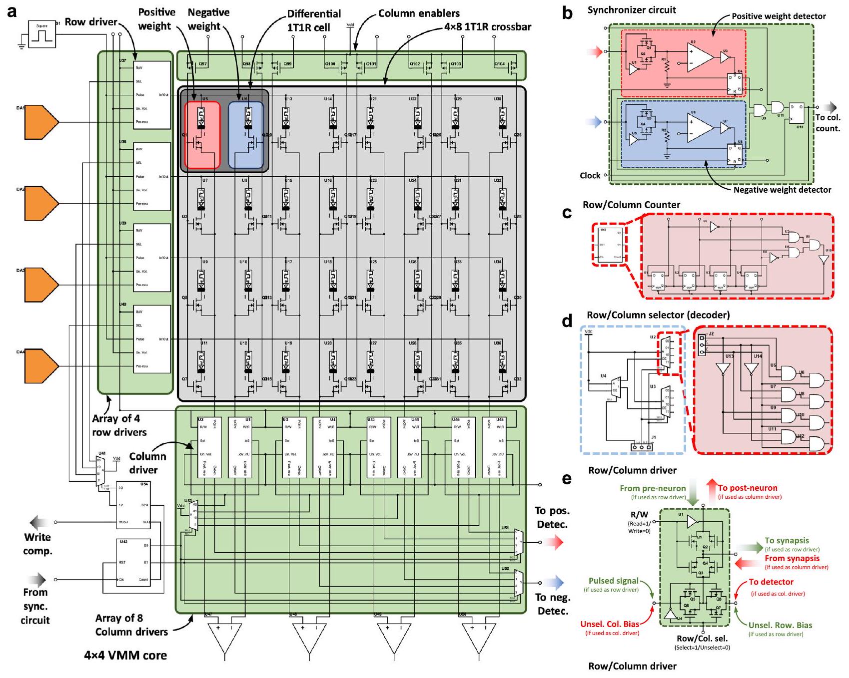
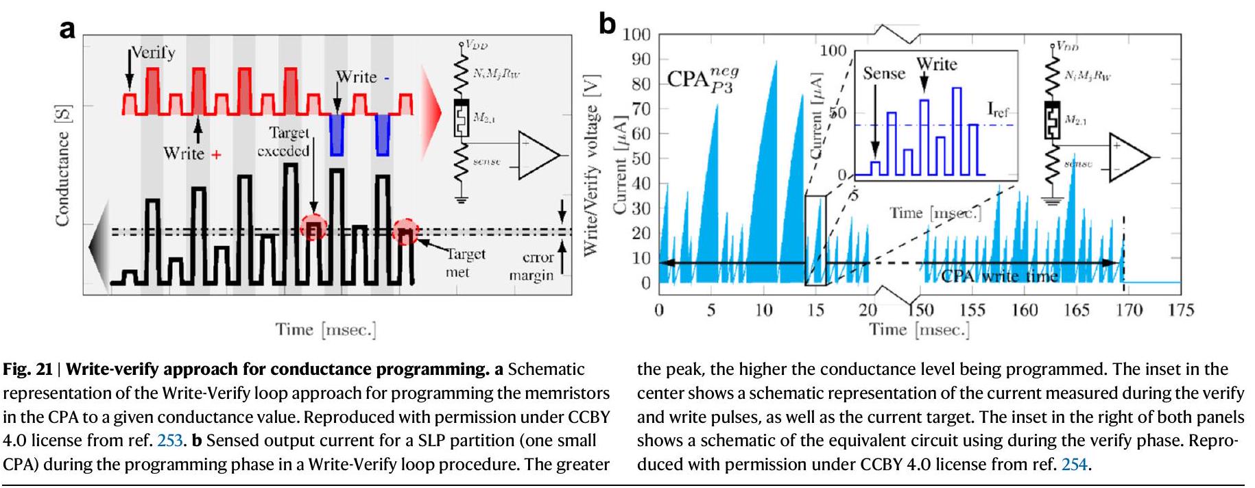
لتمكين الميمريستور المعنون بواسطة كتلة العنوان. سائق الصف والعمود، المستخدم لتطبيق الجهد على الصفوف أو مع إشارة البرمجة، ولربط الأعمدة بالعصبونات الناتجة (أثناء الاستدلال) أو مضخم الإشارة (أثناء التحقق من الكتابة).
تم حسابها عبر MATLAB. تتكون هذه الدائرة المحيطية من كتلة عنوان تقاطع، ومفككات عناوين الصفوف/الأعمدة، ومحددات الصفوف/الأعمدة، وكتلة تأكيد الكتابة (انظر الشكل التكميلي 9c على اليمين والشكل 19a). كتلة عنوان التقاطع (crossbar-AB) هي دائرة تنتج نبضة في كل مرة يتم فيها كتابة الميمريستور الموجود في موضع {i,j} بالكامل في جميع الأقسام (وبذلك تعمل كعداد، كما هو موضح في الشكل 19b)، مما يؤدي إلى نبضات الإخراج (المتعلقة بعدد الميمريستور في كل من أقسام NP). يتم توليد هذه النبضات (بواسطة مضخم استشعار يتكون من مقارن ودائرة قفل كما هو موضح في الشكل 19c) وتنتشر إلى وحدة فك تشفير الأعمدة في الشبكة المتقاطعة (crossbar-CD). تعتبر وحدة فك تشفير الأعمدة في الشبكة المتقاطعة عدادًا غير متزامن بأربعة مخرجات متوازية (انظر الشكل 19d) تُستخدم للإشارة، في كود ثنائي، إلى أي عمود يجب العنوان خلال حلقة كتابة-تحقق البرمجة. أيضًا، تقوم وحدة فك تشفير الأعمدة بإخراج نبضة في كل مرة يتم فيها استلام 10 نبضات، والتي يمكن اعتبارها أيضًا نبضة في كل مرة يتم فيها برمجة صف بالكامل. تُرسل هذه النبضة إلى وحدة فك تشفير الصفوف في الشبكة المتقاطعة (crossbar-RD)، والتي هي عداد مشابه ولكن مع مخرجات متوازية وبالتالي مدخلات التحكم، مع كونه أقرب عدد صحيح أكبر من ). يتم بعد ذلك نقل رموز الصف والعمود المعنيين إلى محدد الصف/ العمود في الشبكة المتقاطعة (crossbar-RS/crossbar-CS). تتكون كتل crossbar-RS و crossbar-CS من مرحلتين. المرحلة الأولى، الموضحة في
الشكل 19d، هو مفرغ رقمي مع مدخلات التحكم (لشبكة تقاطع تحتوي على 10 أعمدة، مدخل التحكم هو رمز مكون من 4 بت) ويمكن تعميمه على أنه أقرب عدد صحيح أعلى من ، مع عدد الصفوف/الأعمدة). بالنسبة لإدخال التحكم المعطى، يكون أحد المخرجات المتوازية نشطًا في وقت واحد فقط. وبالتالي، ينتج عن ذلك متجه عمودي متفرق بحجم 10 (crossbar-CD) أو (العارضة-RD). المرحلة الثانية هي مصفوفة عمودية من 10 (العارضة-CD) أو (crossbarRD) لمفاتيح التناظرية التي تربط عقدة الإدخال لكل صف من صفوف الكروس بار إلى أو (لإشارة إلى تلك الصف المحدد أثناء إجراء الكتابة)، (إذا كانت صف آخر يتم التعامل معه) أو إلى (عندما تكون الشبكة العصبية الاصطناعية تعمل في حالة الاستدلال). محدد العمود هو مصفوفة مشابهة تربط أعمدة عقد الإخراج بمضخم استشعار (مضخم استشعار، مضخم تيار متكامل متصل بمقارن جهد) إذا كانت تلك العمود المحدد يتم التعامل معه، أو (إذا كان يتم معالجة عمود آخر). يتكون كل من هذه المفاتيح التناظرية من 4 خلايا بوابة تمرير، كما هو موضح في الشكل 19e. يوضح الشكل 19a صورة أكبر لهذا المفهوم الأخير، مشيرًا إلى كيفية اتصال المMultiplexor في كتل محدد الصف/العمود مع مجموعة المفاتيح التناظرية، التي تتصل في النهاية بكتلة العبور. بعد أن يقوم كود MATLAB بإنشاء قائمة الشبكة، يتم تمريرها إلى محاكي SPICE الذي يقيم توزيع الجهد والتيار في دائرة العبور ثم يعيد الشكل الموجي الناتج إلى MATLAB.
الشكل 20 | تمثيل تخطيطي لـ متجهات عمودية من الفولتية التناظرية يتم تغذيتها إلى SLP. تم تمثيل 4 حالات: يتوافق مع التصنيف الصحيح للصور من الفئات و على التوالي (لـ
على سبيل المثال، في حالة قاعدة بيانات MNIST، قد تكون صورًا للأرقام ‘5’ و ‘6’ و ‘4’. توضح الحالة d حالة التصنيف الخاطئ، حيث يتوافق أعلى تيار حالي مع الإخراج لصورة من الفئة .
روتين لاستخراج المقاييس (الشكل التوضيحي التكميلي 9d). في هذا المثال، تم تصميم جميع الدوائر المحيطية المتصلة بالشبكة باستخدام عملية CMOS تجارية متاحة بدقة 130 نانومتر، والتي يتوفر نموذجها في مكتبات SPICE.

محاكاة SPICE واستخراج المقاييس

إجراء الاستدلال. بين إجراءات الاستدلال والكتابة، يكون الاستدلال أبسط. خلال هذه المرحلة، يتم تقديم كل صورة اختبار من مجموعة البيانات بشكل متسلسل إلى مدخلات SLP كمتجه عمودي. بحجم حيث كل عنصر من عناصره هو جهد كهربائي ضمن النطاق [ ] (انظر الشكل التوضيحي التكميلي 9). كل من هذه المتجهات الصورية تنتج تيارًا عبر خطوط الكلمات وخطوط البت، حيث تتدفق عبر الميمريستور (المشابك الاصطناعية). اعتمادًا على قوة هذه المشابك، سيكون التيار مرتفعًا (مشبك قوي – موصلية ميمريستور عالية) أو منخفضًا (مشبك ضعيف – موصلية ميمريستور منخفضة). يتم استشعار التيار الكلي المتدفق من كل خط بت في الشبكة عند مخرج خط البت. بالنسبة لمجموعة بيانات مع الفصول (أي قيم الخرج الممكنة)، ومع الأخذ في الاعتبار ترميز تفاضلي (أي، يتم تمثيل كل وزن تشابكي باستخدام 2 ميمريستور) شبكة تقاطع مع يتطلب خطوط البت، مما يؤدي إلى إخراج إشارات التيار. الفكرة الرئيسية وراء مرحلة الاستدلال هي أنه بالنسبة لصورة مدخلة من فئة التيار المتدفق من خط البت ستكون الأعلى. وبالمثل، بالنسبة للفصول و ستكون خطوط البت ذات التيار الأقصى و تم تقديم تمثيل تخطيطي لهذا السلوك في الشكل 20. كما هو موضح، توجد حالة الصور المصنفة بشكل خاطئ، والتي تتوافق مع أعلى تيار لصورة من الفئة لم يتم توفيره بواسطة العمود اختيار أعلى تيار في وقت معين يتم تنفيذ ذلك خارج الموقع (أي عبر MATLAB) من خلال معالجة المسارات الحالية المسجلة. يمكن تنفيذ ذلك بسهولة على الشريحة من خلال تضمين softargmax( دائرة CMOS كما تم مناقشتها في قسم وظيفة SoftArgMax (الكتلة 8). يجب تخصيص هذه الكتلة لنطاق التيار الناتج الديناميكي، حيث يعتمد ذلك على حجم الشبكة ومقاومة الخطوط.
لدراسة مرحلة الاستدلال، تم تعريف مقاييس مختلفة وتم تقسيمها إلى مجموعتين، يمكن الإشارة إليهما على النحو التالي: (i) مقاييس التعرف على الأنماط (وهي الخصائص الجوهرية لـ SLP أو ANN وتم تقديمها في الجدول 2 والشكل 14) و (ii) القياسات الكهربائية (المتعلقة بالتنفيذ الخاص القائم على الميمريستور لـ SLP). تتضمن المجموعة الثانية نطاق متوسط ​​تيار الخرج، واستهلاك الطاقة للعبور (مفيد ليس فقط لتلبية متطلبات الطاقة للعبور، ولكن أيضًا لتحديد مكان حدوث فقدان الطاقة: في التوصيلات).
أو في الميمريستورز)، نسبة الإشارة إلى الضوضاء لإشارات التيار الناتجة، زمن الاستدلال، هوامش القراءة والكتابة (أي، الجزء من الجهد المطبق في مدخلات الشبكة المتقاطعة الذي يصل فعليًا إلى الميمريستورز أثناء عمليات القراءة أو الكتابة) والتردد التشغيلي الأقصى للدائرة العصبية الكاملة (الشبكة المتقاطعة بالإضافة إلى إلكترونيات CMOS).
إجراء الكتابة والتحقق. خلال عملية الكتابة، يتم التعامل مع كل ميمريستور في الشبكة المتقاطعة ( ) يتم توجيهها بشكل فردي وتزويدها بسلسلة من نبضات القراءة والكتابة المتناوبة ذات السعة و على التوالي، مما يتسبب في زيادة تدريجية (أو نقصان) في موصلية الميمريستور. يتم تنفيذ مثل هذا الإجراء العنواني وفقًا لـ النهج لأنه يقلل من اضطراب الخط . ضمن هذه الطريقة في الكتابة، يتم تعيين الصفوف غير المعنونة إلى مصدر ثابت من القيمة . وبالمثل، يتم تأريض عقدة الإخراج من عمود الميمريستور المعنون من خلال مضخم الاستشعار، الذي يقيس التيار المتدفق من هذا العمود (الأعمدة الأخرى عند ). هذا التيار يتناسب مع نبضات الجهد المطبقة وموصلية الميمريستور بالإضافة إلى مقاومة الأسلاك الطفيلية المقابلة للجهاز المعنون ( ). هذا يسمح بتقدير موصلية الميمريستور المعنون. يتم تمثيل هذه العملية بواسطة الدائرة المعادلة المبسطة الموضحة في الإطار في الشكل 21.
قبل بدء عملية الكتابة، نقوم بترجمة مصفوفة الموصلية لكل قسم إلى مصفوفة تيارات، عن طريق ضرب كل عنصر في . بهذه الطريقة، نحصل على كمية قابلة للقياس لكل من العناصر في مصفوفة الموصلية. الهدف من دورة الكتابة هو زيادة موصلية عنصر معين في الشبكة المتقاطعة تدريجياً حتى نشعر بأن التيار المتدفق من خلاله قد وصل إلى القيمة المحددة من قبل مصفوفة التيارات لنفس الموضع (القيمة المستهدفة)، مما يعني أن الموصلية المطلوبة قد تم الوصول إليها أيضًا. تبدأ عملية الكتابة للميمريستور المعنون عن طريق استشعار تيار الإخراج خلال نبضة القراءة للجهد . في حالة كان هذا التيار أقل من القيمة المستهدفة ( )، يتم تطبيق نبضة كتابة للجهد ( )، مما يتسبب في زيادة في موصلية . ثم يتم تطبيق نبضة قراءة جديدة، ويتم استشعار التيار مرة أخرى. تستمر هذه العملية بشكل تكراري حتى يلتقي التيار المستشعر خلال نبضة القراءة بالقيمة المستهدفة. بمجرد الوصول إليها، يقوم مضخم الاستشعار بإخراج نبضة تشير إلى اكتمال إجراء الكتابة للميمريستور المعنون ( )، مما يوقف سلسلة نبضات القراءة/الكتابة ويعد الأجهزة التالية ليتم برمجتها.
من الجدير بالذكر أن العمارة المقسمة تسمح بالبرمجة المتزامنة لـ الميمريستور لجميع الأقسام باستخدام دائرة تحكم أصغر. لنفترض أن الأجهزة التي سيتم برمجتها هي الميمريستورات من شبكة متقاطعة مع NP أقسام، مثل تلك المعروضة في الشكل التكميلي 9d. في هذه الحالة، سيكون الإخراج من مفكك صفوف ( مخرجات) هو الإخراج النشط الوحيد، بالإضافة إلى الإخراج (10 مخرجات) من مفكك الأعمدة. ثم يتم تمرير هذه المتجهات المخرجة إلى كل محدد صف/عمود، الذي يختار في الوقت نفسه الميمريستور في كل شبكة متقاطعة. هذا يتسبب في توصيل جميع الصفوف بسلسلة من نبضات القراءة والكتابة المتناوبة وتوصيل جميع الأعمدة بمضخم استشعار القسم (كل قسم من الشبكة المتقاطعة لديه مضخم استشعار خاص به). جميع الصفوف والأعمدة الأخرى متصلة بـ . يتم استشعار التيار المتدفق من خلال كل من الميمريستورات (وبالتالي خارج الأعمدة ) بواسطة مضخم الاستشعار المرتبط به حتى يتم تحقيق قيمة الموصلية المستهدفة لذلك الميمريستور . ثم يقوم مضخم الاستشعار المرتبط بنشر نبضة تأكيد (ACK) إلى كتلة تأكيد الكتابة، التي تقوم بعد ذلك بفصل الميمريستور المعنون عن مولد نبضات الكتابة لمنع المزيد من تعزيز/خفض موصلية الميمريستور. تنتظر هذه الكتلة نبضات ACK من مضخمات الاستشعار لكل قسم. بمجرد استلام جميع نبضات ACK، يعتبر موضع لجميع الشبكات المتقاطعة قد تم كتابته بنجاح، وعندما تتلقى كتلة تأكيد الكتابة نبضة الساعة التالية للنظام، instructs كتلة عنوان الشبكة المتقاطعة لتوجيه الميمريستور وتبدأ سلسلة الكتابة مرة أخرى. تستمر هذه العملية حتى تقوم كتلة عنوان الشبكة المتقاطعة بتوجيه جميع مواضع الميمريستور في أقسام الشبكة المتقاطعة ( مواضع).
تساعد الشبكات العصبية الميمريستية في تقليل نقل البيانات النموذجي من المعالجات الرقمية، من خلال إجراء الحسابات محليًا داخل الذاكرة. ومع ذلك، فإن هذه الأنظمة تواجه تحديات فريدة خاصة بها لا تزال تحد من تطويرها الإضافي. لاستغلال المزايا الجوهرية للحساب القائم على الشبكة المتقاطعة، فإن التصميم الدقيق لهيكل النظام أمر حاسم، حيث أن الدوائر المحيطية CMOS تصبح عنق زجاجة تعيق تحسين الطاقة والمساحة والكمون الذي يمكن أن تحققه الحوسبة داخل الذاكرة. هدف رئيسي في تصميم هذه الهياكل هو الحفاظ على هذه الزيادة المحيطية إلى الحد الأدنى دون التضحية بالأداء. ومع ذلك، وعلى الرغم من أن مفهوم المسرعات العصبية التناظرية قد تم التحقيق فيه على مدار العقد الماضي، إلا أن الأوراق التي تبلغ عن ميمريستورات هجينة كاملة على الشريحة بدأت تظهر فقط في العامين الماضيين. وبالتالي، يجب تحليل مقاييس الأداء المستمدة من الأنظمة التي تعتمد بشكل كبير على الإلكترونيات الخارجية بعناية.
بينما يتم إجراء الحسابات في الشبكة المتقاطعة في المجال التناظري، يتم استخدام الترميز الرقمي للتوجيه/المعالجة الخارجية. على الرغم من أن كل كتلة في الدائرة المحيطية تتطلب جهدًا كبيرًا من تلقاء نفسها، فإن التحويل بين المجالات التناظرية والرقمية يشكل التحدي الرئيسي في تصميم الشبكة العصبية الميمريستية. يتم تحقيق ذلك من خلال المحولات التناظرية إلى الرقمية والمحولات الرقمية إلى التناظرية، والتجارة الأساسية التي يجب القيام بها في تصميم شبكة عصبية ميمريستية هي تلك بين كفاءة الطاقة والدقة: تأتي الدقة العالية على حساب زيادة استهلاك الطاقة من السيليكون ADC/DAC. ومع ذلك، هناك طرق مختلفة لتقليل هذه الزيادة، مثل ترميز الأوزان لتقليل دقة ADC، من خلال تقنيات التعددية لمخرجات الشبكة المتقاطعة أو تقليل عدد الحالات المتاحة في الميمريستورات. نظرًا للزيادة التي تفرضها ADCs، تشير خيار آخر نحو نهج تناظري بالكامل، مما يدفع الحدود التناظرية/الرقمية نحو نهاية الشبكة العصبية: تبقى بعض الهياكل رقمية في الغالب باستخدام مدخلات ثنائية وأوزان كمية/ثنائية لـ VMM؛ يعتبر البعض مدخلات وأوزان تناظرية، لكن ناتج VMM يتم رقمنته ومعالجته على الفور في المجال الرقمي؛ وآخرون تقريبًا بالكامل تناظري، حيث تحدث الرقمنة فقط بعد وظائف التنشيط وكتل softargmax().
بعيدًا عن دوائر CMOS المطلوبة للمعالجة المسبقة/اللاحقة للإشارات، فإن أداء الشبكات العصبية الميمريستية مهدد أيضًا بالعيوب غير المثالية المتأصلة في هندسة الشبكة المتقاطعة والأجهزة الذاكرة الفردية في الشبكة المتقاطعة. تؤثر الخصائص الفيزيائية غير المثالية للأجهزة على موثوقية الشبكة العصبية الميمريستية وقابليتها للتوسع ودقتها وكمونها واستهلاك الطاقة. تلعب عدد حالات الموصلية المتاحة، وخطية التعزيز والاكتئاب دورًا أساسيًا في إجراء تحديث الوزن وتحدد المتطلبات الأساسية للدائرة المحيطية CMOS المسؤولة عن تنفيذ هذه العملية. وبالتالي، فإن التصميم المشترك للأجهزة والعتاد (أي تحسين خصائص الجهاز بناءً على قدرات الدائرة، والعكس صحيح) أمر لا غنى عنه، وأداة قوية لتمكين هذه العملية هي المحاكاة الكهربائية الواقعية للأنظمة الهجينة CMOS/ميمريستور.
تسمح محاكاة الشبكات العصبية الميمريستية بمعالجة مشاكل التصميم قبل التصنيع وكذلك تقدير الأداء الافتراضي القابل للتحقيق من خلال تقنية ميمريستور معينة. اعتمادًا على المتطلبات، يمكن أن تتراوح من مستوى تجريدي عالٍ، مع القليل (إن وجد) من الاتصال بالأجهزة الفعلية، وصولاً إلى مستوى الدائرة، باستخدام نماذج سلوكية مضغوطة قياسية SPICE/Verilog لأجهزة CMOS والميمريستورات. بين هذين الطرفين، هناك طرق مختلفة على مستوى المعاملات التي تأخذ في الاعتبار مستوى متغير من التفاصيل لتمثيل كل من هيكل الشبكة العصبية الميمريستية وكذلك
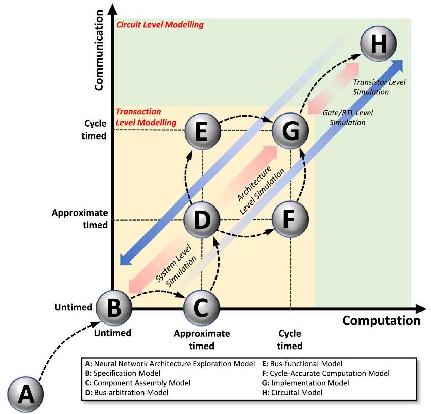
التواصل بينهم. يعتمد اختيار تقنية المحاكاة الأكثر ملاءمة على متطلبات مرحلة التصميم المحددة: كلما اقتربت من مرحلة الطباعة، زادت دقة المحاكاة المطلوبة (يمكن تحقيقها من خلال محاكاة مستوى الدائرة)، بينما في مراحل التصميم المبكرة، يكفي نموذج مستوى النظام للحصول على تقدير سريع للأداء القابل للتحقيق في الشبكات العصبية الاصطناعية الكبيرة والمعقدة. في أي حال، فإن الجمع بشكل صحيح بين هذه الأدوات المختلفة للمحاكاة سيؤدي في النهاية إلى تحسين وتطوير الشبكات العصبية الميمريستيفية.

توفر البيانات

أمثلة الشيفرة المقدمة في المعلومات التكميلية متاحة للجمهور على https://github.com/aguirref/supplementary_ANN_ الخوارزميات.

توفر الشيفرة

مجموعة بيانات MNIST المستخدمة في تصنيف الصور في هذه الدراسة متاحة علنًا على https://yann.lecun.com/exdb/mnist.

References

  1. European Commission, Harnessing the economic benefits of Artificial Intelligence. Digital Transformation Monitor, no. November, 8, 2017.
  2. Rattani, A. Reddy, N. and Derakhshani, R. “Multi-biometric Convolutional Neural Networks for Mobile User Authentication,” 2018 IEEE International Symposium on Technologies for Homeland Security, HST 2018, https://doi.org/10.1109/THS.2018. 85741732018.
  3. BBVA, Biometrics and machine learning: the accurate, secure way to access your bank Accessed: Jan. 21, 2024. [Online]. Available: https://www.bbva.com/en/biometrics-and-machine-learning-the-accurate-secure-way-to-access-your-bank/
  4. Amerini, I., Li, C.-T. & Caldelli, R. Social network identification through image classification with CNN. IEEE Access 7, 35264-35273 (2019).
  5. Ingle P. Y. and Kim, Y. G. “Real-time abnormal object detection for video surveillance in smart cities,” Sensors, 22,https://doi.org/10. 3390/s22103862 2022.
  6. Tan, X., Qin, T., F. Soong, and T.-Y. Liu, “A survey on neural speech synthesis,” https://doi.org/10.48550/arxiv.2106.15561 2021.
  7. “ChatGPT: Optimizing language models for dialogue.” Accessed: Feb. 13, 2023. [Online]. Available: https://openai.com/blog/ chatgpt/
  8. Hong, T., Choi, J. A., Lim, K. & Kim, P. Enhancing personalized ads using interest category classification of SNS users based on deep neural networks. Sens. 2021, Vol. 21, Page 199, 21, 199 (2020).
  9. McKee, S. A., Reflections on the memory wall in 2004 Computing Frontiers Conference, 162-167. https://doi.org/10.1145/977091. 9771152004.
  10. Mehonic, A. & Kenyon, A. J. Brain-inspired computing needs a master plan. Nature 604, 255-260 (2022).
  11. Zhang, C. et al. IMLBench: A machine learning benchmark suite for CPU-GPU integrated architectures. IEEE Trans. Parallel Distrib. Syst. 32, 1740-1752 (2021).
  12. Li, F., Ye, Y., Tian, Z. & Zhang, X. CPU versus GPU: which can perform matrix computation faster-performance comparison for basic linear algebra subprograms. Neural Comput. Appl. 31, 4353-4365 (2019).
  13. Farabet, C. Poulet, C., Han, J. Y. and LeCun, Y. CNP: An FPGAbased processor for Convolutional Networks, FPL 09: 19th International Conference on Field Programmable Logic and Applications, 32-37, https://doi.org/10.1109/FPL.2009.5272559 2009.
  14. Farabet, C. et al., NeuFlow: A runtime reconfigurable dataflow processor for vision, IEEE Computer Society Conference on
Computer Vision and Pattern Recognition Workshops, 109-116, https://doi.org/10.1109/CVPRW.2011.5981829 2011.
15. Zhang, C. et al., Optimizing FPGA-based accelerator design for deep convolutional neural networks, FPGA 2015-2015 ACM/ SIGDA International Symposium on Field-Programmable Gate Arrays, 161-170, https://doi.org/10.1145/2684746.2689060 2015.
16. Chakradhar, S., Sankaradas, M., Jakkula, V. and Cadambi, S. A dynamically configurable coprocessor for convolutional neural networks, Proc. Int. Symp. Comput. Archit., 247-257, https://doi. org/10.1145/1815961.1815993 2010.
17. Wei X. et al., Automated systolic array architecture synthesis for high throughput CNN Inference on FPGAs, Proc. Des. Autom. Conf., Part 128280, https://doi.org/10.1145/3061639. 30622072017.
18. Guo, K. et al., Neural Network Accelerator Comparison. Accessed: Jan. 10, 2023. [Online]. Available: https://nicsefc.ee.tsinghua.edu. cn/projects/neural-network-accelerator.html
19. Jouppi, N. P. et al., In-datacenter performance analysis of a tensor processing unit. Proc. Int. Symp. Comput. Archit., Part F128643, 1-12, https://doi.org/10.1145/3079856.3080246.2017,
20. AI Chip – Amazon Inferentia – AWS. Accessed: May 15, 2023. [Online]. Available: https://aws.amazon.com/machine-learning/ inferentia/
21. Talpes, E. et al. Compute solution for Tesla’s full self-driving computer. IEEE Micro 40, 25-35 (2020).
22. Reuther, A. et al, “AI and ML Accelerator Survey and Trends,” 2022 IEEE High Performance Extreme Computing Conference, HPEC 2022, https://doi.org/10.1109/HPEC55821.2022.9926331.2022,
23. Fick, L., Skrzyniarz, S., Parikh, M., Henry, M. B. and Fick, D. “Analog matrix processor for edge AI real-time video analytics,” Dig. Tech. Pap. IEEE Int. Solid State Circuits Conf, 2022-260-262, https://doi. org/10.1109/ISSCC42614.2022.9731773.2022,
24. “Gyrfalcon Unveils Fourth AI Accelerator Chip – EE Times.” Accessed: May 16, 2023. [Online]. Available: https://www. eetimes.com/gyrfalcon-unveils-fourth-ai-accelerator-chip/
25. Sebastian, A., Le Gallo, M., Khaddam-Aljameh, R. and Eleftheriou, E. “Memory devices and applications for in-memory computing,” Nat. Nanotechnol. 2020 15:7, 15, 529-544, https://doi.org/10. 1038/s41565-020-0655-z.
26. Zheng, N. and Mazumder, P. Learning in energy-efficient neuromorphic computing: algorithm and architecture co-design. WileyIEEE Press, Accessed: May 15, 2023. [Online]. Available: https:// ieeexplore.ieee.org/book/8889858 2020.
27. Orchard, G. et al., “Efficient Neuromorphic Signal Processing with Loihi 2,” IEEE Workshop on Signal Processing Systems, SiPS: Design and Implementation, 2021-October, 254-259, https://doi. org/10.1109/SIPS52927.2021.00053.2021,
28. “Microchips that mimic the human brain could make AI far more energy efficient | Science | AAAS.” Accessed: May 15, 2023. [Online]. Available: https://www.science.org/content/article/ microchips-mimic-human-brain-could-make-ai-far-more-energyefficient
29. Davies, M. et al., “Advancing neuromorphic computing with Loihi: A survey of results and outlook,” Proceedings of the IEEE, 109, 911-934,https://doi.org/10.1109/JPROC.2021.3067593.2021,
30. Barnell, M., Raymond, C., Wilson, M., Isereau, D. and Cicotta, C. “Target classification in synthetic aperture radar and optical imagery using loihi neuromorphic hardware,” in 2020 IEEE High Performance Extreme Computing Conference (HPEC), IEEE, 1-6. https://doi.org/10.1109/HPEC43674.2020.9286246.2020,
31. Viale, A., Marchisio, A., Martina, M., Masera, G., and Shafique, M. “CarSNN: An efficient spiking neural network for event-based autonomous cars on the Loihi Neuromorphic Research Processor,” 2021.
32. “Innatera Unveils Neuromorphic AI Chip to Accelerate Spiking Networks – EE Times.” Accessed: May 15, 2023. [Online]. Available: https://www.eetimes.com/innatera-unveils-neuromorphic-ai-chip-to-accelerate-spiking-networks/
33. Pei, J. et al. “Towards artificial general intelligence with hybrid Tianjic chip architecture,”. Nature 572, 106-111 (2019).
34. Merolla, P. A. et al. “A million spiking-neuron integrated circuit with a scalable communication network and interface,”. Science 345, 668-673 (2014).
35. Adam, G. C., Khiat, A., and Prodromakis, T. “Challenges hindering memristive neuromorphic hardware from going mainstream,” Nat. Commun., 9, Nature Publishing Group, 1-4, https://doi.org/10. 1038/s41467-018-07565-4.2018.
36. Sung, C., Hwang, H. & Yoo, I. K. “Perspective: A review on memristive hardware for neuromorphic computation,”. J. Appl. Phys. 124, 15 (2018).
37. Deng, L. et al. Energy consumption analysis for various memristive networks under different learning strategies,”. Phys. Lett. Sect. A: Gen. At. Solid State Phys. 380, 903-909 (2016).
38. Yu, S., Wu, Y., Jeyasingh, R., Kuzum, D. & Wong, H. S. P. “An electronic synapse device based on metal oxide resistive switching memory for neuromorphic computation,”. IEEE Trans. Electron Dev. 58, 2729-2737 (2011).
39. Shulaker, M. M. et al. “Three-dimensional integration of nanotechnologies for computing and data storage on a single chip,”. Nature 547, 74-78 (2017).
40. Li, C. et al. Three-dimensional crossbar arrays of self-rectifying Si/ SiO2/Si memristors. Nat. Commun. 2017 8:1 8, 1-9 (2017).
41. Yoon, J. H. et al. “Truly electroforming-free and low-energy memristors with preconditioned conductive tunneling paths,”. Adv. Funct. Mater. 27, 1702010 (2017).
42. Choi, B. J. et al. “High-speed and low-energy nitride memristors,”. Adv. Funct. Mater. 26, 5290-5296 (2016).
43. Strukov, D. B., Snider, G. S., Stewart, D. R. and Williams, R. S. “The missing memristor found,” Nature, 453,80-83, https://doi.org/10. 1038/nature06932.
44. “FUJITSU SEMICONDUCTOR MEMORY SOLUTION.” Accessed: Nov. 16, 2022. [Online]. Available: https://www.fujitsu.com/jp/ group/fsm/en/
45. “Everspin | The MRAM Company.” Accessed: Nov. 16, 2022. [Online]. Available: https://www.everspin.com/
46. “Yole Group.” Accessed: Nov. 16, 2022. [Online]. Available: https://www.yolegroup.com/?cn-reloaded=1
47. Stathopoulos, S. et al. “Multibit memory operation of metal-oxide Bi-layer memristors,”. Sci. Rep. 7, 1-7 (2017).
48. Wu, W. et al., “Demonstration of a multi-level -range bulk switching ReRAM and its application for keyword spotting,” Technical Digest – International Electron Devices Meeting, IEDM, 2022-December, 1841-1844, https://doi.org/10.1109/IEDM45625. 2022.10019450.2022,
49. Yang, J. et al., “Thousands of conductance levels in memristors monolithically integrated on CMOS,” https://doi.org/10.21203/ RS.3.RS-1939455/V1.2022,
50. Goux, L. et al., “Ultralow sub-500nA operating current highperformance TiNไAl TiN bipolar RRAM achieved through understanding-based stack-engineering,” Digest of Technical Papers – Symposium on VLSI Technology, 159-160, https://doi.org/10.1109/VLSIT.2012.6242510 2012
51. Li, H. et al. “Memristive crossbar arrays for storage and computing applications,”. Adv. Intell. Syst. 3, 2100017 (2021).
52. Lin, P. et al. “Three-dimensional memristor circuits as complex neural networks,”. Nat. Electron. 3, 225-232 (2020).
53. Ishii, M. et al., “On-Chip Trainable 1.4M 6T2R PCM synaptic array with 1.6K Stochastic LIF neurons for spiking RBM,” Technical Digest – International Electron Devices Meeting, IEDM, 2019-
310-313, 2019, https://doi.org/10.1109/IEDM19573.2019. 8993466.
54. Li, C. et al. “Efficient and self-adaptive in-situ learning in multilayer memristor neural networks,”. Nat. Commun. 9, 1-8 (2018).
55. Yao, P. et al. “Fully hardware-implemented memristor convolutional neural network,”. Nature 577, 641-646 (2020).
56. Correll, J. M. et al., “An 8-bit 20.7 TOPS/W Multi-Level Cell ReRAMbased Compute Engine,” in 2022 IEEE Symposium on VLSI Technology and Circuits (VLSI Technology and Circuits), IEEE, 264-265. https://doi.org/10.1109/VLSITechnologyandCir46769.2022. 9830490.2022,
57. Cai, F. et al., “A fully integrated reprogrammable memristorCMOS system for efficient multiply-accumulate operations,” Nat Electron, 2, no. July, 290-299, [Online]. Available: https://doi.org/ 10.1038/s41928-019-0270-x 2019.
58. Hung, J.-M., “An 8-Mb DC-Current-Free Binary-to-8b Precision ReRAM Nonvolatile Computing-in-Memory Macro using Time-Space-Readout with 1286.4-21.6TOPS/W for Edge-AI Devices,” in 2022 IEEE International Solid- State Circuits Conference (ISSCC), IEEE, 1-3. https://doi.org/10.1109/ISSCC42614.2022.9731715.2022,
59. Xue, C.-X., “15.4 A 22 nm 2 Mb ReRAM Compute-in-Memory Macro with 121-28TOPS/W for Multibit MAC Computing for Tiny AI Edge Devices,” in 2020 IEEE International Solid- State Circuits Conference – (ISSCC), IEEE, 2020, 244-246.
60. Wan, W. et al. “A compute-in-memory chip based on resistive random-access memory,”. Nature 608, 504-512 (2022).
61. Yin, S., Sun, X., Yu, S. & Seo, J. S. “High-throughput in-memory computing for binary deep neural networks with monolithically integrated RRAM and 90-nm CMOS,”. IEEE Trans. Electron. Dev. 67, 4185-4192 (2020).
62. Yan, X. et al. “Robust Ag/ZrO2/WS2/Pt Memristor for Neuromorphic Computing,”. ACS Appl Mater. Interfaces 11, 48029-48038 (2019).
63. Chen, Q. et al, “Improving the recognition accuracy of memristive neural networks via homogenized analog type conductance quantization,” Micromachines, 11, https://doi.org/10.3390/ MI11040427.2020,
64. Wang, Y. “High on/off ratio black phosphorus based memristor with ultra-thin phosphorus oxide layer,” Appl. Phys. Lett., 115, https://doi.org/10.1063/1.5115531.2019,
65. Xue, F. et al. “Giant ferroelectric resistance switching controlled by a modulatory terminal for low-power neuromorphic in-memory computing,”. Adv. Mater. 33, 1-12 (2021).
66. Pan, W.-Q. et al. “Strategies to improve the accuracy of memristorbased convolutional neural networks,”. Trans. Electron. Dev., 67, 895-901 (2020).
67. Seo, S. et al. “Artificial optic-neural synapse for colored and colormixed pattern recognition,”. Nat. Commun. 9, 1-8 (2018).
68. Chandrasekaran, S., Simanjuntak, F. M., Saminathan, R., Panda, D. and Tseng, T. Y., “Improving linearity by introducing Al in as a memristor synapse device,” Nanotechnology, 30, https://doi.org/ 10.1088/1361-6528/ab3480.2019,
69. Zhang, B. et al. ” yield production of polymer nano-memristor for in-memory computing,”. Nat. Commun. 12, 1-11 (2021).
70. Feng, X. et al. “Self-selective multi-terminal memtransistor crossbar array for in-memory computing,”. ACS Nano 15, 1764-1774 (2021).
71. Khaddam-Aljameh, R.et al. “HERMES-Core-A1.59-TOPS/mm2PCM on CMOS in-memory compute core using 300-ps/LSB linearized CCO-based ADCs,”. IEEE J. Solid-State Circuits 57, 1027-1038 (2022).
72. Narayanan, P. et al. “Fully on-chip MAC at 14 nm enabled by accurate row-wise programming of PCM-based weights and parallel vector-transport in duration-format,”. IEEE Trans. Electron Dev. 68, 6629-6636 (2021).
73. Le Gallo, M. et al., “A 64-core mixed-signal in-memory compute chip based on phase-change memory for deep neural network inference,” 2022, Accessed: May 09, 2023. [Online]. Available: https://arxiv.org/abs/2212.02872v1
74. Murmann, B. “Mixed-signal computing for deep neural network inference,”. IEEE Trans. Very Large Scale Integr. VLSI Syst. 29, 3-13 (2021).
75. Yin, S., Jiang, Z., Seo, J. S. & Seok, M. “XNOR-SRAM: In-memory computing SRAM macro for binary/ternary deep neural networks,”. IEEE J. Solid-State Circuits 55, 1733-1743 (2020).
76. Biswas, A. & Chandrakasan, A. P. “CONV-SRAM: An energyefficient SRAM with in-memory dot-product computation for lowpower convolutional neural networks,”. IEEE J. Solid-State Circuits 54, 217-230 (2019).
77. Valavi, H., Ramadge, P. J., Nestler, E. & Verma, N. “A 64-Tile 2.4-Mb In-memory-computing CNN accelerator employing chargedomain compute,”. IEEE J. Solid-State Circuits 54, 1789-1799 (2019).
78. Khwa, W. S. et al. “A 65 nm 4 Kb algorithm-dependent computing-in-memory SRAM unit-macro with 2.3 ns and 55.8TOPS/W fully parallel product-sum operation for binary DNN edge processors,”. Dig. Tech. Pap. IEEE Int. Solid State Circuits Conf. 61, 496-498 (2018).
79. Verma, N. et al. “In-memory computing: advances and prospects,”. IEEE Solid-State Circuits Mag. 11, 43-55 (2019).
80. Diorio, C., Hasler, P., Minch, A. & Mead, C. A. “A single-transistor silicon synapse,”. IEEE Trans. Electron. Dev. 43, 1972-1980 (1996).
81. Merrikh-Bayat, F. et al. “High-performance mixed-signal neurocomputing with nanoscale floating-gate memory cell arrays,”. IEEE Trans. Neural Netw. Learn Syst. 29, 4782-4790 (2018).
82. Wang, P. et al. “Three-dimensional NAND flash for vector-matrix multiplication,”. IEEE Trans. Very Large Scale Integr. VLSI Syst. 27, 988-991 (2019).
83. Bavandpour, M., Sahay, S., Mahmoodi, M. R. & Strukov, D. B. “3DaCortex: an ultra-compact energy-efficient neurocomputing platform based on commercial 3D-NAND flash memories,”. Neuromorph. Comput. Eng. 1, 014001 (2021).
84. Chu, M. et al. “Neuromorphic hardware system for visual pattern recognition with memristor array and CMOS neuron,”. IEEE Trans. Ind. Electron. 62, 2410-2419 (2015).
85. Yeo, I., Chu, M., Gi, S. G., Hwang, H. & Lee, B. G. “Stuck-at-fault tolerant schemes for memristor crossbar array-based neural networks,”. IEEE Trans. Electron Devices 66, 2937-2945 (2019).
86. LeCun, Y., Cortes, C., and Burges, C. J. C., “MNIST handwritten digit database of handwritten digits.” Accessed: Nov. 21, 2019. [Online]. Available: http://yann.lecun.com/exdb/mnist/
87. Krizhevsky, A., Nair, V., and Hinton, G. “The CIFAR-10 dataset.” Accessed: Apr. 04, 2023. [Online]. Available: https://www.cs. toronto.edu/~kriz/cifar.html
88. Deng, J. et al., “ImageNet: A large-scale hierarchical image database,” in 2009 IEEE Conference on Computer Vision and Pattern Recognition, IEEE, 2009, 248-255.
89. Simonyan, K. and Zisserman, A. “Very deep convolutional networks for large-scale image recognition,” 2014.
90. He, K., Zhang, X., Ren, S. and Sun, J. “Deep Residual Learning for Image Recognition,” in 2016 IEEE Conference on Computer Vision and Pattern Recognition (CVPR), IEEE, 770-778. https://doi.org/10. 1109/CVPR.2016.90.2016,
91. Chen, P. Y., Peng, X. & Yu, S. “NeuroSim: A circuit-level macro model for benchmarking neuro-inspired architectures in online learning,”. IEEE Trans. Comput.-Aided Des. Integr. Circuits Syst. 37, 3067-3080 (2018).
92. Wang, Q., Wang, X., Lee, S. H., Meng, F.-H. and Lu W. D., “A Deep Neural Network Accelerator Based on Tiled RRAM Architecture,” in
2019 IEEE International Electron Devices Meeting (IEDM), IEEE, 14.4.114.4.4. https://doi.org/10.1109/IEDM19573.2019.8993641.2019,
93. Kim, H., Mahmoodi, M. R., Nili, H. & Strukov, D. B. “4K-memristor analog-grade passive crossbar circuit,”. Nat. Commun. 12, 1-11 (2021).
94. Inc. The Mathworks, “MATLAB.” Natick, Massachusetts, 2019.
95. Amirsoleimani, A. et al. “In-memory vector-matrix multiplication in monolithic complementary metal-oxide-semiconductor-memristor integrated circuits: design choices, challenges, and perspectives,”. Adv. Intell. Syst. 2, 2000115, https://doi.org/10.1002/ AISY. 202000115 (2020).
96. Chakraborty, I. et al. “Resistive crossbars as approximate hardware building blocks for machine learning: opportunities and challenges,”. Proc. IEEE 108, 2276-2310 (2020).
97. Jain, S. et al. “Neural network accelerator design with resistive crossbars: Opportunities and challenges,”. IBM J. Res Dev. 63, 6 (2019).
98. Ankit, A. et al. “PANTHER: A Programmable Architecture for Neural Network Training Harnessing Energy-Efficient ReRAM,”. IEEE Trans. Comput. 69, 1128-1142 (2020).
99. Mochida, R. et al. “A 4M synapses integrated analog ReRAM based 66.5 TOPS/W neural-network processor with cell current controlled writing and flexible network architecture,” Digest of Technical Papers – Symposium on VLSI Technology, 175-176, Oct. 2018, 2018
100. Su, F. et al., “A 462 GOPs/J RRAM-based nonvolatile intelligent processor for energy harvesting loE system featuring nonvolatile logics and processing-in-memory,” Digest of Technical Papers Symposium on VLSI Technology, C260-C261, https://doi.org/10. 23919/VLSIT.2017.7998149.2017,
101. Han J. and Orshansky, M. “Approximate computing: An emerging paradigm for energy-efficient design,” in 2013 18th IEEE European Test Symposium (ETS), IEEE, 1-6. https://doi.org/10.1109/ETS. 2013.6569370.2013,
102. Kiani, F., Yin, J., Wang, Z., Joshua Yang, J. & Xia, Q. “A fully hardware-based memristive multilayer neural network,”. Sci. Adv. 7, 4801 (2021).
103. Gokmen, T. and Vlasov, Y. “Acceleration of deep neural network training with resistive cross-point devices: Design considerations,” Front. Neurosci., 10, no. JUL, https://doi.org/10.3389/fnins.2016. 00333.2016,
104. Fouda, M. E., Lee, S., Lee, J., Eltawil, A. & Kurdahi, F. “Mask technique for fast and efficient training of binary resistive crossbar arrays,”. IEEE Trans. Nanotechnol. 18, 704-716 (2019).
105. Prezioso, M. et al. “Training and operation of an integrated neuromorphic network based on metal-oxide memristors,”. Nature 521, 61-64 (2015).
106. Hu, M. et al. “Memristor crossbar-based neuromorphic computing system: A case study,”. IEEE Trans. Neural Netw. Learn Syst. 25, 1864-1878 (2014).
107. Hu, M. et al., “Dot-product engine for neuromorphic computing,” in DAC ’16: Proceedings of the 53rd Annual Design Automation Conference, New York, NY, USA: Association for Computing Machinery, 1-6. https://doi.org/10.1145/2897937.2898010.2016,
108. Liu, C., Hu, M., Strachan, J. P. and Li, H. H. “Rescuing memristorbased neuromorphic design with high defects,” in 2017 54th ACM/ EDAC/IEEE Design Automation Conference (DAC), Institute of Electrical and Electronics Engineers Inc., https://doi.org/10.1145/ 3061639.3062310.2017.
109. Romero-Zaliz, R., Pérez, E., Jiménez-Molinos, F., Wenger, C. & Roldán, J. B. “Study of quantized hardware deep neural networks based on resistive switching devices, conventional versus convolutional approaches,”. Electronics 10, 1-14 (2021).
110. Pérez, E. et al. “Advanced temperature dependent statistical analysis of forming voltage distributions for three different HfO 2 –
based RRAM technologies,”. Solid State Electron. 176, 107961 (2021).
111. Pérez-Bosch Quesada, E. et al. “Toward reliable compact modeling of multilevel 1T-1R RRAM devices for neuromorphic systems,”. Electronics 10, 645 (2021).
112. Xia, L. et al. “Stuck-at Fault Tolerance in RRAM Computing Systems,”. IEEE J. Emerg. Sel. Top. Circuits Syst., 8, 102-115 (2018).
113. Li, C. et al., “CMOS-integrated nanoscale memristive crossbars for CNN and optimization acceleration,” 2020 IEEE International Memory Workshop, IMW 2020 – Proceedings, https://doi.org/10. 1109/IMW48823.2020.9108112.2020,
114. Pedretti, G. et al. “Redundancy and analog slicing for precise inmemory machine learning – Part I: Programming techniques,”. IEEE Trans. Electron. Dev. 68, 4373-4378 (2021).
115. Pedretti, G. et al. “Redundancy and analog slicing for precise inmemory machine learning – Part II: Applications and benchmark,”. IEEE Trans. Electron. Dev. 68, 4379-4383 (2021).
116. Wang, Z. et al. “Fully memristive neural networks for pattern classification with unsupervised learning,”. Nat. Electron. 1, 137-145 (2018).
117. T. Rabuske and J. Fernandes, “Charge-Sharing SAR ADCs for lowvoltage low-power applications,” https://doi.org/10.1007/978-3-319-39624-8.2017,
118. Kumar, P. et al. “Hybrid architecture based on two-dimensional memristor crossbar array and CMOS integrated circuit for edge computing,”. npj 2D Mater. Appl. 6, 1-10 (2022).
119. Krestinskaya, O., Salama, K. N. & James, A. P. “Learning in memristive neural network architectures using analog backpropagation circuits,”. IEEE Trans. Circuits Syst. I: Regul. Pap. 66, 719-732 (2019).
120. Chua, L. O., Tetzlaff, R. and Slavova, A. Eds., Memristor Computing Systems. Springer International Publishing, https://doi.org/10. 1007/978-3-030-90582-8.2022.
121. Oh, S. et al. “Energy-efficient Mott activation neuron for fullhardware implementation of neural networks,”. Nat. Nanotechnol. 16, 680-687 (2021).
122. Ambrogio, S. et al. “Equivalent-accuracy accelerated neuralnetwork training using analogue memory,”. Nature 558, 60-67 (2018).
123. Bocquet, M. et al., “In-memory and error-immune differential RRAM implementation of binarized deep neural networks,” Technical Digest – International Electron Devices Meeting, IEDM, 20.6.120.6.4, Jan. 2019, https://doi.org/10.1109/IEDM.2018. 8614639.2018,
124. Cheng, M. et al., “TIME: A Training-in-memory architecture for Memristor-based deep neural networks,” Proc. Des. Autom. Conf., Part 12828, 0-5, https://doi.org/10.1145/3061639. 3062326.2017,
125. Chi, P. et al., “PRIME: A novel processing-in-memory architecture for neural network computation in ReRAM-based main memory,” Proceedings – 2016 43rd International Symposium on Computer Architecture, ISCA 2016, 27-39, https://doi.org/10.1109/ISCA. 2016.13.2016,
126. Krestinskaya, O., Choubey, B. & James, A. P. “Memristive GAN in Analog,”. Sci. Rep. 2020 10:1 10, 1-14 (2020).
127. Li, G. H. Y. et al., “All-optical ultrafast ReLU function for energyefficient nanophotonic deep learning,” Nanophotonics, https:// doi.org/10.1515/NANOPH-2022-0137/ASSET/GRAPHIC/J_ NANOPH-2022-0137_FIG_007.JPG.2022,
128. Ando, K. et al. “BRein memory: a single-chip binary/ternary reconfigurable in-memory deep neural network accelerator achieving 1.4 TOPS at 0.6 W,”. IEEE J. Solid-State Circuits 53, 983-994 (2018).
129. Price, M., Glass, J. & Chandrakasan, A. P. “A scalable speech recognizer with deep-neural-network acoustic models and voice-
activated power gating,”. Dig. Tech. Pap. IEEE Int Solid State Circuits Conf. 60, 244-245 (2017).
130. Yin, S. et al., “A 1.06-to-5.09 TOPS/W reconfigurable hybrid-neural-network processor for deep learning applications,” IEEE Symposium on VLSI Circuits, Digest of Technical Papers, C26-C27, https://doi.org/10.23919/VLSIC.2017.8008534.2017,
131. Chen, Y. H., Krishna, T., Emer, J. S. & Sze, V. “Eyeriss: An energyefficient reconfigurable accelerator for deep convolutional neural networks,”. IEEE J. Solid-State Circuits 52, 127-138 (2017).
132. Lazzaro, J., Ryckebusch, S. M., Mahowald, A. and Mead, C. A. “Winner-Take-All Networks of O(N) Complexity,” in Advances in Neural Information Processing Systems, D. Touretzky, Ed., MorganKaufmann, 1988.
133. Andreou, A. G. et al. “Current-mode subthreshold MOS circuits for analog VLSI neural systems,”. IEEE Trans. Neural Netw. 2, 205-213 (1991).
134. Pouliquen, P. O., Andreou, A. G., Strohbehn, K. and Jenkins, R. E. “Associative memory integrated system for character recognition,” Midwest Symposium on Circuits and Systems, 1, 762-765, https://doi.org/10.1109/MWSCAS.1993.342935.1993,
135. Starzyk, J. A. & Fang, X. “CMOS current mode winner-take-all circuit with both excitatory and inhibitory feedback,”. Electron. Lett. 29, 908-910 (1993).
136. DeWeerth, S. P. & Morris, T. G. “CMOS current mode winner-takeall circuit with distributed hysteresis,”. Electron. Lett. 31, 1051-1053 (1995).
137. Indiveri, G. “A current-mode hysteretic winner-take-all network, with excitatory and inhibitory coupling,”. Analog Integr. Circuits Signal Process 28, 279-291 (2001).
138. Tan, B. P. & Wilson, D. M. “Semiparallel rank order filtering in analog VLSI,”. IEEE Trans. Circuits Syst. II: Analog Digit. Signal Process. 48, 198-205 (2001).
139. Serrano, T. & Linares-Barranco, B. “Modular current-mode highprecision winner-take-all circuit,”. Proc. – IEEE Int. Symp. Circuits Syst. 5, 557-560 (1994).
140. Meador, J. L. and Hylander, P. D. “Pulse Coded Winner-Take-All Networks,” Silicon Implementation of Pulse Coded Neural Networks, 79-99, https://doi.org/10.1007/978-1-4615-2680-3_5.1994,
141. El-Masry, E. I., Yang, H. K. & Yakout, M. A. “Implementations of artificial neural networks using current-mode pulse width modulation technique,”. IEEE Trans. Neural Netw. 8, 532-548 (1997).
142. Choi, J. & Sheu, B. J. “A high-precision vlsi winner-take-all circuit for self-organizing neural networks,”. IEEE J. Solid-State Circuits 28, 576-584 (1993).
143. Yu, H. & Miyaoka, R. S. “A High-Speed and High-Precision Winner-Select-Output (WSO) ASIC,”. IEEE Trans. Nucl. Sci. 45, 772-776 (1998). PART 1.
144. Lau, K. T. and Lee, S. T. “A CMOS winner-takes-all circuit for selforganizing neural networks,” https://doi.org/10.1080/ 002072198134896, 84, 131-136, 2010
145. He, Y. & Sánchez-Sinencio, E. “Min-net winner-take-all CMOS implementation,”. Electron Lett. 29, 1237-1239 (1993).
146. Demosthenous, A., Smedley, S. & Taylor, J. “A CMOS analog winner-take-all network for large-scale applications,”. IEEE Trans. Circuits Syst. I: Fundam. Theory Appl. 45, 300-304 (1998).
147. Pouliquen, P. O., Andreou, A. G. & Strohbehn, K. “Winner-Takes-All associative memory: A hamming distance vector quantizer,”. Analog Integr. Circuits Signal Process. 1997 13:1 13, 211-222 (1997).
148. Fish, A., Milrud, V. & Yadid-Pecht, O. “High-speed and highprecision current winner-take-all circuit,”. IEEE Trans. Circuits Syst. II: Express Briefs 52, 131-135 (2005).
149. Ohnhäuser, F. “Analog-Digital Converters for Industrial Applications Including an Introduction to Digital-Analog Converters,” 2015.
150. Pavan, S., Schreier, R.. and Temes, G. C. “Understanding DeltaSigma Data Converters.”.
151. Walden, R. H. “Analog-to-digital converter survey and analysis,”. IEEE J. Sel. Areas Commun. 17, 539-550 (1999).
152. Harpe, P., Gao, H., Van Dommele, R., Cantatore, E. & Van Roermund, A. H. M. “A 0.20 mm 23 nW signal acquisition IC for miniature sensor nodes in 65 nm CMOS. IEEE J. Solid-State Circuits 51, 240-248 (2016).
153. Murmann, B. “ADC Performance Survey 1997-2022.” Accessed: Sep. 05, 2022. [Online]. Available: http://web.stanford.edu/ ~murmann/adcsurvey.html.
154. Ankit, A. et al., “PUMA: A Programmable Ultra-efficient Memristorbased Accelerator for Machine Learning Inference,” International Conference on Architectural Support for Programming Languages and Operating Systems – ASPLOS, 715-731, https://doi.org/10. 1145/3297858.3304049.2019,
155. Ni, L. et al., “An energy-efficient matrix multiplication accelerator by distributed in-memory computing on binary RRAM crossbar,” Proceedings of the Asia and South Pacific Design Automation Conference, ASP-DAC, 25-28-January-2016, 280-285, https://doi. org/10.1109/ASPDAC.2016.7428024.2016,
156. Wang, X., Wu, Y. and Lu, W. D. “RRAM-enabled AI Accelerator Architecture,” in 2021 IEEE International Electron Devices Meeting (IEDM), IEEE, 12.2.1-12.2.4. https://doi.org/10.1109/IEDM19574. 2021.9720543.2021,
157. Xiao, T. P. et al. On the Accuracy of Analog Neural Network Inference Accelerators. [Feature],” IEEE Circuits Syst. Mag. 22, 26-48 (2022).
158. Sun, X. et al, “XNOR-RRAM: A scalable and parallel resistive synaptic architecture for binary neural networks,” Proceedings of the 2018 Design, Automation and Test in Europe Conference and Exhibition, DATE 2018, 2018-January, 1423-1428, https://doi.org/ 10.23919/DATE.2018.8342235.2018,
159. Zhang, W. et al. “Neuro-inspired computing chips,”. Nat. Electron. 2020 3:7 3, 371-382 (2020).
160. Shafiee, A. et al., “ISAAC: A Convolutional Neural Network Accelerator with In-Situ Analog Arithmetic in Crossbars,” in Proceedings – 2016 43rd International Symposium on Computer Architecture, ISCA 2016, Institute of Electrical and Electronics Engineers Inc., 14-26. https://doi.org/10.1109/ISCA.2016.12.2016,
161. Fujiki, D., Mahlke, S. and Das, R. “In-memory data parallel processor,” in ACM SIGPLAN Notices, New York, NY, USA: ACM, 1-14. https://doi.org/10.1145/3173162.3173171.2018,
162. Nourazar, M., Rashtchi, V., Azarpeyvand, A. & Merrikh-Bayat, F. “Memristor-based approximate matrix multiplier,”. Analog. Integr. Circuits Signal Process 93, 363-373 (2017).
163. Saberi, M., Lotfi, R., Mafinezhad, K. & Serdijn, W. A. “Analysis of power consumption and linearity in capacitive digital-to-analog converters used in successive approximation ADCs,”. IEEE Trans. Circuits Syst. I: Regul. Pap. 58, 1736-1748 (2011).
164. Kull, L. et al. “A single-Channel asynchronous SAR ADC with alternate comparators for enhanced speed in 32 nm digital SOI CMOS,”. IEEE J. Solid-State Circuits 48, 3049-3058 (2013).
165. Hagan, M., Demuth, H., Beale, M. and De Jesús, O. Neural Network Design, 2nd ed. Stillwater, OK, USA: Oklahoma State University, 2014.
166. Choi, S., Sheridan, P. & Lu, W. D. “Data clustering using memristor networks,”. Sci. Rep. 5, 1-10 (2015).
167. Khaddam-Aljameh, R. et al., “HERMES Core: A 14 nm CMOS and PCM-based In-Memory Compute Core using an array of LSB Linearized CCO-based ADCs and local digital processing,” in 2021 Symposium on VLSI Technology, Kyoto, Japan: IEEE, 978-982. Accessed: Jan. 21, 2024. [Online]. Available: https:// ieeexplore.ieee.org/document/9508706
168. Kennedy, J. and Eberhart, R. “Particle swarm optimization,” Proceedings of ICNN’95 – International Conference on Neural Networks, 4, https://doi.org/10.1109/ICNN.1995.488968. 1942-1948,
169. Goldberg, D. E. & Holland, J. H. “Genetic Algorithms and machine learning. Mach. Learn. 3, 95-99 (1988).
170. Kirkpatrick, S., Gelatt, C. D. & Vecchi, M. P. “Optimization by simulated annealing,”. Science 220, 671-680 (1983).
171. Rumelhart, D. E., Hinton, G. E. & Williams, R. J. “Learning representations by back-propagating errors,”. Nature 323, 533-536 (1986).
172. Dennis, J. E. and Schnabel, R. B. Numerical Methods for Unconstrained Optimization and Nonlinear Equations. Society for Industrial and Applied Mathematics, https://doi.org/10.1137/1. 9781611971200.1996.
173. Møller, M. F. “A scaled conjugate gradient algorithm for fast supervised learning,”. Neural Netw. 6, 525-533 (1993).
174. Powell, M. J. D. “Restart procedures for the conjugate gradient method,”. Math. Program. 12, 241-254 (1977).
175. Fletcher, R. “Function minimization by conjugate gradients,”. Comput. J. 7, 149-154 (1964).
176. Marquardt, D. W. “An algorithm for least-squares estimation of nonlinear parameters,”. J. Soc. Ind. Appl. Math. 11, 431-441 (1963).
177. Riedmiller, M. and Braun, H. “Direct adaptive method for faster backpropagation learning: The RPROP algorithm,” in 1993 IEEE International Conference on Neural Networks, Publ by IEEE, 586-591. https://doi.org/10.1109/icnn.1993.298623.1993,
178. Battiti, R. “First- and second-order methods for learning: between steepest descent and Newton’s Method,”. Neural Comput. 4, 141-166 (1992).
179. Bottou, L. “Stochastic gradient descent tricks,” Lecture Notes in Computer Science (including subseries Lecture Notes in Artificial Intelligence and Lecture Notes in Bioinformatics), 7700 LECTURE NO, 421-436, https://doi.org/10.1007/978-3-642-35289-8_25/ COVER.2012,
180. Li, M., Zhang, T., Chen, Y. and Smola, A. J. “Efficient mini-batch training for stochastic optimization,” Proceedings of the ACM SIGKDD International Conference on Knowledge Discovery and Data Mining, 661-670, https://doi.org/10.1145/2623330. 2623612.2014,
181. Zamanidoost, E., Bayat, F. M., Strukov, D. and Kataeva, I. “Manhattan rule training for memristive crossbar circuit pattern classifiers,” WISP 2015 – IEEE International Symposium on Intelligent Signal Processing, Proceedings, https://doi.org/10.1109/WISP. 2015.7139171.2015,
182. Duchi, J., Hazan, E. & Singer, Y. “Adaptive subgradient methods for online learning and stochastic optimization,”. J. Mach. Learn. Res. 12, 2121-2159 (2011).
183. “Neural Networks for Machine Learning – Geoffrey Hinton – C. Cui’s Blog.” Accessed: Nov. 21, 2022. [Online]. Available: https:// cuicaihao.com/neural-networks-for-machine-learning-geoffreyhinton/
184. Kingma, D. P. and Ba, J. L. “Adam: A Method for Stochastic Optimization,” 3rd International Conference on Learning Representations, ICLR 2015 – Conference Track Proceedings, 2014, https://doi. org/10.48550/arxiv.1412.6980.
185. Zeiler, M. D. “ADADELTA: An adaptive learning rate method,” Dec. 2012, https://doi.org/10.48550/arxiv.1212.5701.
186. Xiong, X. et al. “Reconfigurable logic-in-memory and multilingual artificial synapses based on 2D heterostructures,”. Adv. Funct. Mater. 30, 2-7 (2020).
187. Zoppo, G., Marrone, F. & Corinto, F. “Equilibrium propagation for memristor-based recurrent neural networks,”. Front Neurosci. 14, 1-8 (2020).
188. Alibart, F., Zamanidoost, E. & Strukov, D. B. “Pattern classification by memristive crossbar circuits using ex situ and in situ training,”. Nat. Commun. 4, 1-7 (2013).
189. Joshi, V. et al., “Accurate deep neural network inference using computational phase-change memory,” Nat Commun, 11, https:// doi.org/10.1038/s41467-020-16108-9.2020,
190. Rasch, M. J. et al., “Hardware-aware training for large-scale and diverse deep learning inference workloads using in-memory computing-based accelerators,” 2023.
191. Huang, H.-M., Wang, Z., Wang, T., Xiao, Y. & Guo, X. “Artificial neural networks based on memristive devices: from device to system,”. Adv. Intell. Syst. 2, 2000149 (2020).
192. Nandakumar, S. R. et al., “Mixed-precision deep learning based on computational memory,” Front. Neurosci., 14, https://doi.org/10. 3389/fnins.2020.00406.2020,
193. Le Gallo, M. et al. “Mixed-precision in-memory computing,”. Nat. Electron. 1, 246-253 (2018).
194. Yao, P. et al., “Face classification using electronic synapses,” Nat. Commun., 8, May, 1-8, https://doi.org/10.1038/ ncomms15199.2017,
195. Papandreou, N. et al., “Programming algorithms for multilevel phase-change memory,” Proceedings – IEEE International Symposium on Circuits and Systems, 329-332, https://doi.org/10.1109/ ISCAS.2011.5937569.2011,
196. Milo, V. et al., “Multilevel HfO2-based RRAM devices for lowpower neuromorphic networks,” APL Mater, 7, https://doi.org/10. 1063/1.5108650.2019,
197. Yu, S. et al., “Scaling-up resistive synaptic arrays for neuroinspired architecture: Challenges and prospect,” in Technical Digest – International Electron Devices Meeting, IEDM, Institute of Electrical and Electronics Engineers Inc., 17.3.1-17.3.4. https://doi. org/10.1109/IEDM.2015.7409718.2015,
198. Woo, J. et al. “Improved synaptic behavior under identical pulses using AlOx/HfO2 bilayer RRAM array for neuromorphic systems,”. IEEE Electron. Device Lett. 37, 994-997 (2016).
199. Xiao, S. et al. “GST-memristor-based online learning neural networks,”. Neurocomputing 272, 677-682 (2018).
200. Tian, H. et al. “A novel artificial synapse with dual modes using bilayer graphene as the bottom electrode,”. Nanoscale 9, 9275-9283 (2017).
201. Shi, T., Yin, X. B., Yang, R. & Guo, X. “Pt/WO3/FTO memristive devices with recoverable pseudo-electroforming for time-delay switches in neuromorphic computing,”. Phys. Chem. Chem. Phys. 18, 9338-9343 (2016).
202. Menzel, S. et al. “Origin of the ultra-nonlinear switching kinetics in oxide-based resistive switches,”. Adv. Funct. Mater. 21, 4487-4492 (2011).
203. Buscarino, A., Fortuna, L., Frasca, M., Gambuzza, L. V. and Sciuto, G., “Memristive chaotic circuits based on cellular nonlinear networks,” https://doi.org/10.1142/SO218127412500708, 22,3, 2012
204. Li, Y. & Ang, K.-W. “Hardware implementation of neuromorphic computing using large-scale memristor crossbar arrays,”. Adv. Intell. Syst. 3, 2000137 (2021).
205. Zhu, J., Zhang, T., Yang, Y. & Huang, R. “A comprehensive review on emerging artificial neuromorphic devices,”. Appl Phys. Rev. 7, 011312 (2020).
206. Wang, Z. et al. “Engineering incremental resistive switching in TaOx based memristors for brain-inspired computing,”. Nanoscale 8, 14015-14022 (2016).
207. Park, S. M. et al. “Improvement of conductance modulation linearity in a -Doped memristor through the increase of the number of oxygen vacancies,”. ACS Appl. Mater. Interfaces 12, 1069-1077 (2020).
208. Slesazeck, S. & Mikolajick, T. “Nanoscale resistive switching memory devices: a review,”. Nanotechnology 30, 352003 (2019).
209. Waser, R., Dittmann, R., Staikov, C. & Szot, K. “Redox-based resistive switching memories nanoionic mechanisms, prospects, and challenges,”. Adv. Mater. 21, 2632-2663 (2009).
210. Ielmini, D. and Waser, R. Resistive Switching. Weinheim, Germany: Wiley-VCH Verlag GmbH & Co. KGaA, 2016.
211. Wouters, D. J., Waser, R. & Wuttig, M. “Phase-change and redoxbased resistive switching memories,”. Proc. IEEE 103, 1274-1288 (2015).
212. Pan, F., Gao, S., Chen, C., Song, C. & Zeng, F. “Recent progress in resistive random access memories: Materials, switching mechanisms, and performance,”. Mater. Sci. Eng. R: Rep. 83, 1-59 (2014).
213. Kim, S. et al. “Analog synaptic behavior of a silicon nitride memristor,”. ACS Appl Mater. Interfaces 9, 40420-40427 (2017).
214. Li, W., Sun, X., Huang, S., Jiang, H. & Yu, S. “A 40-nm MLC-RRAM compute-in-memory macro with sparsity control, On-Chip Writeverify, and temperature-independent ADC references,”. IEEE J. Solid-State Circuits 57, 2868-2877 (2022).
215. Buchel, J. et al., “Gradient descent-based programming of analog in-memory computing cores,” Technical Digest – International Electron Devices Meeting, IEDM, 3311-3314, 2022, https://doi.org/ 10.1109/IEDM45625.2022.10019486.2022,
216. Prezioso, M. et al. “Spike-timing-dependent plasticity learning of coincidence detection with passively integrated memristive circuits,”. Nat. Commun. 9, 1-8 (2018).
217. Park, S. et al., “Electronic system with memristive synapses for pattern recognition,” Sci. Rep., 5, https://doi.org/10.1038/ srep10123.2015,
218. Yu, S. et al., “Binary neural network with 16 Mb RRAM macro chip for classification and online training,” in Technical Digest – International Electron Devices Meeting, IEDM, Institute of Electrical and Electronics Engineers Inc., 16.2.1-16.2.4. https://doi.org/10.1109/ IEDM.2016.7838429.2017,
219. Chen, W. H. et al. “CMOS-integrated memristive non-volatile computing-in-memory for AI edge processors,”. Nat. Electron. 2, 420-428 (2019).
220. Chen, W. H. et al., “A 16 Mb dual-mode ReRAM macro with sub14ns computing-in-memory and memory functions enabled by self-write termination scheme,” Technical Digest – International Electron Devices Meeting, IEDM, 28.2.1-28.2.4, 2018,
221. Hu, M. et al., “Memristor-based analog computation and neural network classification with a dot product engine,” Adv. Mater., 30, https://doi.org/10.1002/adma.201705914.2018,
222. Li, C. et al. Analogue signal and image processing with large memristor crossbars. Nat. Electron 1, 52-59 (2018).
223. Paszke A. et al., “Automatic differentiation in PyTorch”.
224. Abadi, M. et al., “TensorFlow: Large-Scale Machine Learning on Heterogeneous Systems,” 2015.
225. Stimberg, M., Brette, R. and Goodman, D. F. M. “Brian 2, an intuitive and efficient neural simulator,” Elife, 8, https://doi.org/10.7554/ ELIFE.47314.2019,
226. Spreizer, S. et al., “NEST 3.3,” Mar. 2022, https://doi.org/10.5281/ ZENODO. 6368024.
227. Hazan, H. et al. “BindsNET: A machine learning-oriented spiking neural networks library in python,”. Front Neuroinform 12, 89 (2018).
228. M. Y. Lin et al., “DL-RSIM: A simulation framework to enable reliable ReRAM-based accelerators for deep learning,” IEEE/ACM International Conference on Computer-Aided Design, Digest of Technical Papers, ICCAD, https://doi.org/10.1145/3240765. 3240800.2018,
229. Sun, X. & Yu, S. “Impact of non-ideal characteristics of resistive synaptic devices on implementing convolutional neural networks,”. IEEE J. Emerg. Sel. Top. Circuits Syst. 9, 570-579 (2019).
230. Ma, X. et al., “Tiny but Accurate: A Pruned, Quantized and Optimized Memristor Crossbar Framework for Ultra Efficient DNN Implementation,” Proceedings of the Asia and South Pacific Design Automation Conference, ASP-DAC, 2020-Janua, 301-306, https:// doi.org/10.1109/ASP-DAC47756.2020.9045658.2020,
231. Yuan, G. et al., “An Ultra-Efficient Memristor-Based DNN Framework with Structured Weight Pruning and Quantization Using ADMM,” Proceedings of the International Symposium on Low Power Electronics and Design, 2019, https://doi.org/10.1109/ ISLPED.2019.8824944.2019.
232. Rasch, M. J. et al., “A flexible and fast PyTorch toolkit for simulating training and inference on analog crossbar arrays,” 2021 IEEE 3rd International Conference on Artificial Intelligence Circuits and Systems, AICAS 2021, https://doi.org/10. 48550/arxiv.2104.02184.2021,
233. Grötker, T., “System design with SystemC,” 217, 2002.
234. Gajski, D. D. “SpecC: specification language and methodology,” 313, 2000.
235. Lee, M. K. F. et al. “A system-level simulator for RRAM-based neuromorphic computing chips,”. ACM Trans. Archit. Code Optim. (TACO) 15, 4 (2019).
236. BanaGozar, A. et al. “System simulation of memristor based computation in memory platforms,”. Lect. Notes Comput. Sci. (Subser. Lect. Notes Artif. Intell. Lect. Notes Bioinforma.) 12471, 152-168 (2020).
237. Gai, L. and Gajski, D. “Transaction level modeling: an overview,” Hardware/Software Codesign – Proceedings of the International Workshop, 19-24, https://doi.org/10.1109/CODESS.2003. 1275250.2003,
238. Poremba, M. and Xie, Y. “NVMain: An architectural-level main memory simulator for emerging non-volatile memories,” Proceedings – 2012 IEEE Computer Society Annual Symposium on VLSI, ISVLSI 2012, 392-397, https://doi.org/10.1109/ISVLSI.2012.82.2012,
239. Poremba, M., Zhang, T. & Xie, Y. “NVMain 2.0: A user-friendly memory simulator to model (non-)volatile memory systems,”. IEEE Comput. Archit. Lett. 14, 140-143 (2015).
240. Xia, L. et al. “MNSIM: Simulation platform for memristor-based neuromorphic computing system,”. IEEE Trans. Comput.-Aided Des. Integr. Circuits Syst. 37, 1009-1022 (2018).
241. Zhu, Z. et al., “MNSIM 2.0: A behavior-level modeling tool for memristor-based neuromorphic computing systems,” in Proceedings of the ACM Great Lakes Symposium on VLSI, GLSVLSI, Association for Computing Machinery, 83-88. https://doi.org/10. 1145/3386263.3407647.2020,
242. Banagozar, A. et al., “CIM-SIM: Computation in Memory SIMulator,” in Proceedings of the 22nd International Workshop on Software and Compilers for Embedded Systems, SCOPES 2019, Association for Computing Machinery, Inc, 1-4. https://doi.org/10. 1145/3323439.3323989.2019,
243. Fei, X., Zhang, Y. & Zheng, W. “XB-SIM: A simulation framework for modeling and exploration of ReRAM-based CNN acceleration design,”. Tsinghua Sci. Technol. 26, 322-334 (2021).
244. Zahedi, M. et al. “MNEMOSENE: Tile architecture and simulator for memristor-based computation-in-memory,”. ACM J. Emerg. Technol. Comput. Syst. 18, 1-24 (2022).
245. Dong, X., Xu, C., Xie, Y. & Jouppi, N. P. “NVSim: A circuit-level performance, energy, and area model for emerging nonvolatile memory,”. IEEE Trans. Comput.-Aided Des. Integr. Circuits Syst. 31, 994-1007 (2012).
246. Song, L., Qian, X., Li, H. and Chen, Y. “PipeLayer: A Pipelined ReRAM-based accelerator for deep learning,” Proceedings –
International Symposium on High-Performance Computer Architecture, 541-552, https://doi.org/10.1109/HPCA.2017.55.2017,
247. Imani, M. et al., “RAPIDNN: In-Memory Deep Neural Network Acceleration Framework,” 2018.
248. Chen, A. “A comprehensive crossbar array model with solutions for line resistance and nonlinear device characteristics,”. IEEE Trans. Electron Devices 60, 1318-1326 (2013).
249. Aguirre, F. L. et al., “Line resistance impact in memristor-based multi layer perceptron for pattern recognition,” in 2021 IEEE 12th Latin American Symposium on Circuits and Systems, LASCAS 2021, Institute of Electrical and Electronics Engineers Inc., Feb. https://doi.org/10.1109/LASCAS51355.2021.9667132.2021.
250. Aguirre, F. L. et al. “Minimization of the line resistance impact on memdiode-based simulations of multilayer perceptron arrays applied to pattern recognition,”. J. Low. Power Electron. Appl. 11, 9 (2021).
251. Lee, Y. K. et al. “Matrix mapping on crossbar memory arrays with resistive interconnects and its use in in-memory compression of biosignals,”. Micromachines 10, 306 (2019).
252. Fei, W., Yu, H., Zhang, W. & Yeo, K. S. “Design exploration of hybrid CMOS and memristor circuit by new modified nodal analysis,”. IEEE Trans. Very Large Scale Integr. VLSI Syst. 20, 1012-1025 (2012).
253. Aguirre, F. L., Pazos, S. M., Palumbo, F., Suñé, J. & Miranda, E. “Application of the quasi-static memdiode model in cross-point arrays for large dataset pattern recognition,”. IEEE Access 8, 1-1 (2020).
254. Aguirre, F. L., Pazos, S. M., Palumbo, F., Suñé, J. & Miranda, E. “SPICE simulation of RRAM-based crosspoint arrays using the dynamic memdiode model,”. Front Phys. 9, 548 (2021).
255. Aguirre, F. L. et al. “Assessment and improvement of the pattern recognition performance of memdiode-based cross-point arrays with randomly distributed stuck-at-faults,”. Electron. 10, 2427 (2021).
256. Fritscher, M., Knodtel, J., Reichenbach, M. and Fey, D. “Simulating memristive systems in mixed-signal mode using commercial design tools,” 2019 26th IEEE International Conference on Electronics, Circuits and Systems, ICECS 2019, 225-228, https://doi. org/10.1109/ICECS46596.2019.8964856.2019,
257. Applied Materials, “Ginestra .” [Online]. Available: http://www. appliedmaterials.com/mdlx
258. “TCAD – Technology Computer Aided Design (TCAD) | Synopsys.” Accessed: Jan. 20, 2023. [Online]. Available: https://www. synopsys.com/silicon/tcad.html
259. Krestinskaya, O., Salama, K. N. & James, A. P. “Automating analogue AI chip design with genetic search,”. Adv. Intell. Syst. 2, 2000075 (2020).
260. Krestinskaya, O., Salama, K. and James, A. P. “Towards hardware optimal neural network selection with multi-objective genetic search,” Proceedings – IEEE International Symposium on Circuits and Systems, 2020, 2020, https://doi.org/10.1109/ISCAS45731. 2020.9180514/VIDEO.
261. Guan, Z. et al., “A hardware-aware neural architecture search pareto front exploration for in-memory computing,” in 2022 IEEE 16th International Conference on Solid-State & Integrated Circuit Technology (ICSICT), IEEE, 1-4. https://doi.org/10.1109/ ICSICT55466.2022.9963263.2022,
262. Li, G., Mandal, S. K., Ogras, U. Y. and Marculescu, R. “FLASH: Fast neural architecture search with hardware optimization,” ACM Trans. Embed. Compu. Syst., 20, https://doi.org/10.1145/ 3476994.2021,
263. Yuan, Z. et al. “NAS4RRAM: neural network architecture search for inference on RRAM-based accelerators,”. Sci. China Inf. Sci. 64, 160407 (2021).
264. Yan, Z., Juan, D.-C., Hu, X. S. and Shi, Y. “Uncertainty modeling of emerging device based computing-in-memory neural accelerators with application to neural architecture search,” in Proceedings of the 26th Asia and South Pacific Design Automation Conference, New York, NY, USA: ACM, 859-864. https://doi.org/ 10.1145/3394885.3431635.2021,
265. Sun H. et al., “Gibbon: Efficient co-exploration of NN model and processing-in-memory architecture,” in 2022 Design, Automation & Test in Europe Conference & Exhibition (DATE), IEEE, 867-872. https://doi.org/10.23919/DATE54114.2022. 9774605.2022,
266. Jiang, W. et al. Device-circuit-architecture co-exploration for computing-in-memory neural accelerators. IEEE Trans. Comput. 70, 595-605 (2021).
267. Burr, G. W. et al. Experimental demonstration and tolerancing of a large-scale neural network (165 000 Synapses) using phasechange memory as the synaptic weight element. IEEE Trans. Electron Devices 62, 3498-3507 (2015).
268. Dong, Z. et al. “Convolutional neural networks based on RRAM devices for image recognition and online learning tasks,”. IEEE Trans. Electron. Dev. 66, 793-801 (2019).
269. Querlioz, D., Bichler, O., Dollfus, P. & Gamrat, C. “Immunity to device variations in a spiking neural network with memristive nanodevices,”. IEEE Trans. Nanotechnol. 12, 288-295 (2013).
270. Guan, X., Yu, S. & Wong, H. S. P. “A SPICE compact model of metal oxide resistive switching memory with variations,”. IEEE Electron. Device Lett. 33, 1405-1407 (2012).
271. Liang, J., Yeh, S., Simon Wong, S. & Philip Wong, H. S. “Effect of wordline/bitline scaling on the performance, energy consumption, and reliability of cross-point memory array,”. ACM J. Emerg. Technol. Comput. Syst. 9, 1-14 (2013).
272. Hirtzlin, T. et al. “Digital biologically plausible implementation of binarized neural networks with differential hafnium oxide resistive memory arrays,”. Front Neurosci. 13, 1383 (2020).
273. Xue, C. X. et al., “A 1Mb Multibit ReRAM computing-in-memory macro with 14.6 ns Parallel MAC computing time for CNN based AI Edge processors,” Dig Tech Pap IEEE Int Solid State Circuits Conf, 2019-February, 388-390, https://doi.org/10.1109/ISSCC.2019. 8662395.2019,
274. Wu, T. F. et al., “A 43pJ/Cycle Non-Volatile Microcontroller with 4.7 s Shutdown/Wake-up Integrating 2.3-bit/Cell Resistive RAM and Resilience Techniques,” Dig Tech Pap IEEE Int Solid State Circuits Conf, 2019-February, 226-228, https://doi.org/10.1109/ ISSCC.2019.8662402.2019,
275. Liu, Q. et al., “A Fully Integrated Analog ReRAM based 78.4TOPS/ W compute-in-memory chip with fully parallel MAC computing,” Dig. Tech. Pap. IEEE Int. Solid State Circuits Conf, 2020-February, 500-502, https://doi.org/10.1109/ISSCC19947.2020. 9062953.2020,
276. Xiao, T. P., Bennett, C. H., Feinberg, B., Agarwal, S. and Marinella, M. J. “Analog architectures for neural network acceleration based on non-volatile memory,” Applied Physics Reviews, 7, American Institute of Physics Inc., https://doi.org/10.1063/1. 5143815.2020.
277. “NVIDIA Data Center Deep Learning Product Performance | NVIDIA Developer.” Accessed: Nov. 28, 2022. [Online]. Available: https:// developer.nvidia.com/deep-learning-performance-traininginference
278. Habana L., “Goya Inference Platform White Paper,” 1-14, 2019.
279. Chen Y. et al., “DaDianNao: A Machine-Learning Supercomputer,” Proceedings of the Annual International Symposium on Microarchitecture, MICRO, 2015-January, no. January, 609-622, https:// doi.org/10.1109/MICRO.2014.58.2015,
280. Lee, J. et al. “UNPU: An energy-efficient deep neural network accelerator with fully variable weight bit precision,”. IEEE J. SolidState Circuits 54, 173-185 (2019).
281. Bankman, D., Yang, L., Moons, B., Verhelst, M. & Murmann, B. “An always-on CIFAR-10 mixed-signal binary CNN processor with all memory on chip in 28 nm CMOS,”. Dig. Tech. Pap. IEEE Int Solid State Circuits Conf. 61, 222-224 (2018).
282. Nag, A. et al. “Newton: Gravitating towards the physical limits of crossbar acceleration,”. IEEE Micro 38, 41-49 (2018).
283. Bojnordi M. N. and Ipek, E. “Memristive Boltzmann machine: A hardware accelerator for combinatorial optimization and deep learning,” Proceedings – International Symposium on HighPerformance Computer Architecture, 2016-April, 1-13, https://doi. org/10.1109/HPCA.2016.7446049.2016,
284. Jain, S. et al. “A heterogeneous and programmable compute-inmemory accelerator architecture for analog-AI using dense 2-D Mesh,”. IEEE Trans. Very Large Scale Integr. VLSI Syst. 31, 114-127 (2023).
285. Carnevale N. T. and Hines, M. L. “The NEURON book,” The NEURON Book, 1-457, https://doi.org/10.1017/ CBO9780511541612.2006,
286. Lammie, C., Xiang, W., Linares-Barranco, B. and Azghadi, M. R. “MemTorch: An Open-source Simulation Framework for Memristive Deep Learning Systems,” 1-14, 2020.
287. Xiao, T. P., Bennett, C. H., Feinberg, B., Marinella, M. J. and Agarwal, S. “CrossSim: accuracy simulation of analog in-memory computing,” https://github.com/sandialabs/cross-sim. Accessed: Sep. 06, 2022. [Online]. Available: https://github.com/ sandialabs/cross-sim
288. Mehonic, A., Joksas, D., Ng, W. H., Buckwell, M. & Kenyon, A. J. “Simulation of inference accuracy using realistic rram devices,”. Front. Neurosci. 13, 1-15 (2019).
289. Zhang, Q. et al. “Sign backpropagation: An on-chip learning algorithm for analog RRAM neuromorphic computing systems,”. Neural Netw. 108, 217-223 (2018).
290. Yamaoka, M. “Low-power SRAM,” in Green Computing with Emerging Memory: Low-Power Computation for Social Innovation, 9781461408123, Springer New York, 59-85. https://doi.org/10. 1007/978-1-4614-0812-3_4/TABLES/4.2013,
291. Starzyk, J. A. and Jan, Y. W. “Voltage based winner takes all circuit for analog neural networks,” Midwest Symposium on Circuits and Systems, 1, 501-504, https://doi.org/10.1109/mwscas.1996. 594211, 1996

الشكر والتقدير

لقد تم دعم هذا العمل من قبل خطة التمويل الأساسية لجامعة الملك عبدالله للعلوم والتقنية. يقر ف.أ. بالدعم المالي من MICINN (إسبانيا) من خلال برنامج خوان دي لا سيرفا – منحة التدريب رقم FJC2O21-046808-I. تم دعم عمل إ.م.، ج.ب.ر.، وج.س. من قبل وزارة العلوم والابتكار، إسبانيا، تحت مشروع PID2O22-139586NB-C41. ف.أ. حاليًا مع شركة Intrinsic Semiconductor Technologies Ltd.، المملكة المتحدة.

مساهمات المؤلفين

كتب ف.أ. و م.ل. الورقة وجمعوا المساهمات المقدمة من المؤلفين المشاركين الآخرين. ساهم أ.إ. و ك.س. بالملاحظة التكميلية 1. ساهم ك.ن.س و أ.ك. بالملاحظة التكميلية 2. راجع ف.أ.، أ.س.، م.ج.، و.س.، ت.و.، ج.ج.ي.، و.ل.، م.-ف.ج.، د.ي.، ي.ي.، أ.م.، أ.ج.ك.، م.أ.ف.، ج.ب.ر.، ي.و.، ه.-ه.ه.، ن.ر.، ج.س.، إ.م.، أ.إ.، ج.س.، ك.س.، ك.ن.س.، أ.ك.، إكس.ي.، ك.و.أ.، س.ج.، س.ل.، أ.ع.، س.ب. و م.ل. بمراجعة المخطوطة.

المصالح المتنافسة

يعلن المؤلفون عدم وجود مصالح متنافسة.

معلومات إضافية

المعلومات التكميلية النسخة الإلكترونية تحتوي على
المواد التكميلية المتاحة على
https://doi.org/10.1038/s41467-024-45670-9.
يجب توجيه المراسلات وطلبات المواد إلى ماريو لانزا.
معلومات مراجعة الأقران تشكر Nature Communications جينا كريستينا آدام، كان لي وإليا فالوف على مساهمتهم في مراجعة الأقران لهذا العمل.
معلومات إعادة الطباعة والتصاريح متاحة على
http://www.nature.com/reprints
ملاحظة الناشر تظل Springer Nature محايدة فيما يتعلق بالمطالبات القضائية في الخرائط المنشورة والانتماءات المؤسسية.
الوصول المفتوح هذه المقالة مرخصة بموجب رخصة المشاع الإبداعي 4.0 الدولية، التي تسمح بالاستخدام والمشاركة والتكيف والتوزيع وإعادة الإنتاج في أي وسيلة أو تنسيق، طالما أنك تعطي الائتمان المناسب للمؤلفين الأصليين والمصدر، وتوفر رابطًا لرخصة المشاع الإبداعي، وتوضح ما إذا كانت هناك تغييرات قد تم إجراؤها. الصور أو المواد الأخرى من طرف ثالث في هذه المقالة مشمولة في رخصة المشاع الإبداعي للمقالة، ما لم يُذكر خلاف ذلك في سطر الائتمان للمادة. إذا لم تكن المادة مشمولة في رخصة المشاع الإبداعي للمقالة واستخدامك المقصود غير مسموح به بموجب اللوائح القانونية أو يتجاوز الاستخدام المسموح به، ستحتاج إلى الحصول على إذن مباشرة من صاحب حقوق الطبع والنشر. لعرض نسخة من هذه الرخصة، قم بزيارة http://creativecommons.org/ licenses/by/4.0/.
© المؤلفون 2024
¹قسم العلوم الفيزيائية والهندسة، جامعة الملك عبدالله للعلوم والتقنية (KAUST)، ثول 23955-6900، المملكة العربية السعودية. قسم الهندسة الإلكترونية، جامعة برشلونة المستقلة (UAB)، 08193 برشلونة، إسبانيا. أبحاث IBM – زيورخ، روتشليكون، سويسرا. قسم الهندسة الكهربائية وهندسة الكمبيوتر، جامعة جنوب كاليفورنيا (USC)، لوس أنجلوس، كاليفورنيا 90089، الولايات المتحدة الأمريكية. قسم الهندسة الكهربائية وعلوم الكمبيوتر، جامعة ميتشيغان، آن آربر، ميشيغان 48109، الولايات المتحدة الأمريكية. قسم الهندسة الكهربائية، جامعة تسينغ هوا الوطنية، هسينتشو 30013، تايوان. قسم الإلكترونيات والمعلومات والهندسة الحيوية، بوليتكنيكو دي ميلانو و IUNET، بيازا ل. دا فينشي 32، 20133 ميلانو، إيطاليا. كلية الهندسة الإلكترونية وهندسة الكمبيوتر، جامعة بكين، شنتشن، الصين. قسم الهندسة الإلكترونية والكهربائية، كلية لندن الجامعية (UCL)، تورينغتون بليس، WC1E 7JE، لندن، المملكة المتحدة. قسم الإلكترونيات وتكنولوجيا الحواسيب، كلية العلوم، جامعة غرناطة، Avenida Fuentenueva s/n، 18071 غرناطة، إسبانيا. عمود تطوير المنتجات الهندسية (EPD)، جامعة سنغافورة للتكنولوجيا والتصميم، 8 طريق سوماباه، 487372 سنغافورة، سنغافورة. قسم علوم الكمبيوتر والهندسة الكهربائية والرياضيات، جامعة الملك عبدالله للعلوم والتقنية (KAUST)، ثول 23955-6900، المملكة العربية السعودية. المختبر الرئيسي للأجهزة والأنظمة العصبية الشبيهة بالدماغ في مقاطعة خبي، جامعة خبي، باودينغ 071002، الصين. قسم الهندسة الكهربائية وهندسة الكمبيوتر، كلية التصميم والهندسة، الجامعة الوطنية في سنغافورة (NUS)، سنغافورة، سنغافورة.

Journal: Nature Communications, Volume: 15, Issue: 1
DOI: https://doi.org/10.1038/s41467-024-45670-9
PMID: https://pubmed.ncbi.nlm.nih.gov/38438350
Publication Date: 2024-03-04

Hardware implementation of memristorbased artificial neural networks

Received: 8 June 2023
Accepted: 1 February 2024
Published online: 04 March 2024
(D) Check for updates

Abstract

Fernando Aguirre , Abu Sebastian © , Manuel Le Gallo © , Wenhao Song , Tong Wang , J. Joshua Yang , Wei Lu , Meng-Fan Chang , Daniele Ielmini , Yuchao Yang © , Adnan Mehonic © , Anthony Kenyon © , Marco A. Villena © , Juan B. Roldán © , Yuting Wu , Hung-Hsi Hsu , Nagarajan Raghavan , Jordi Suñé © , Enrique Miranda , Ahmed Eltawil © , Gianluca Setti , Kamilya Smagulova , Khaled N. Salama © , Olga Krestinskaya © , Xiaobing Yan © , Kah-Wee Ang , Samarth Jain , Sifan Li , Osamah Alharbi © , Sebastian Pazos © & Mario Lanza ©

Abstract

Artificial Intelligence (AI) is currently experiencing a bloom driven by deep learning (DL) techniques, which rely on networks of connected simple computing units operating in parallel. The low communication bandwidth between memory and processing units in conventional von Neumann machines does not support the requirements of emerging applications that rely extensively on large sets of data. More recent computing paradigms, such as high parallelization and near-memory computing, help alleviate the data communication bottleneck to some extent, but paradigm- shifting concepts are required. Memristors, a novel beyond-complementary metal-oxide-semiconductor (CMOS) technology, are a promising choice for memory devices due to their unique intrinsic device-level properties, enabling both storing and computing with a small, massively-parallel footprint at low power. Theoretically, this directly translates to a major boost in energy efficiency and computational throughput, but various practical challenges remain. In this work we review the latest efforts for achieving hardware-based memristive artificial neural networks (ANNs), describing with detail the working principia of each block and the different design alternatives with their own advantages and disadvantages, as well as the tools required for accurate estimation of performance metrics. Ultimately, we aim to provide a comprehensive protocol of the materials and methods involved in memristive neural networks to those aiming to start working in this field and the experts looking for a holistic approach.

The development of sophisticated artificial neural networks (ANNs) has become one of the highest priorities of technological companies and governments of wealthy countries, as they can boost the fabrication of artificial intelligence (AI) systems that generate economic and social benefits in multiple fields (e.g., logistics, commerce, health care,
national security, etc.) . ANNs are able to compute and store the huge amount of electronic data produced (either by humans or machines), and to execute complex operations with them. Examples of electronic products that contain ANNs with which we interact in our daily lives are those that identify biometric patterns (e.g., face, fingerprint) for access
control in smartphones or online banking apps , and those that identify objects in images from social networks and security/traffic cameras . Beyond image recognition, other examples are the engines that convert speech to text in computers and smartphones , natural language processing as for example the novel automated chat system chat-GPT , and those that provide accurate recommendations for online shopping based on previous behaviours from ourselves and/or people in our network .
ANNs can be understood as the implementation of a sequence of mathematical operations. The structure of ANNs consists of multiple nodes (called neurons) interconnected to each other (by synapses), and the learning is implemented by adjusting the strength (weight) of such connections. Modern ANNs are implemented via software in generalpurpose computing systems based on a central processing unit (CPU) and a memory -the so-called Von Neumann architecture . However, in this architecture a large amount of the energy consumption and computing time is related to continuous data exchange between both units, which is not efficient. The computing time can be accelerated by
using graphics processing units (GPUs) to implement the ANNs (see Fig. 1a), as these can perform multiple operations in parallel . However, this approach consumes even more energy, which requires large computing systems and thereby cannot be integrated in mobile devices. Another option is to use field programable gate arrays (FPGAs), which consume much less energy than GPUs while providing an intermediate computing efficiency between CPUs and GPUs . A survey carried out by Guo et al. on the existing hardware solutions for ANN implementation and their performance is condensed in Fig. 1b.
In the past few years, some companies and universities have presented application specific integrated circuits (ASICs) based on the complementary metal oxide semiconductor (CMOS) technology that are capable to compute and store information in the same unit. This allow such ASICs to perform multiple operations in parallel very fast, making them capable of mimicking, directly in the hardware, the behaviour of the neurons and synapses in the ANN. A comprehensive list of these ASICs comprising those such as the Google TPU , Amazon inferentia , Tesla NPU , etc., are summarized in ref. 22. Such integrated
Fig. 1 | Computing power demand increase and platform transition from VonNeumann towards highly parallelized architectures. a The increase in computing power demands over the past four decades expressed in petaFLOPS per days. Until 2012, computing power demand doubled every 24 months; recently this has shortened to approximately every 2 months. The colour legend indicates different
application domains . Mehonic, A., Kenyon, A.J. Brain-inspired computing needs a master plan. Nature 604, 255-260 (2022), reproduced with permission from SNCSC. b A comparison of neural network accelerators for FPGA, ASIC, and GPU devices in terms of speed and power consumption. GOP/s giga operations per second, tera operations per second.
circuits can be grouped in two categories. On one hand, dataflow processors are custom-designed processors for neural network inference and training. Since neural network training and inference computations can be entirely deterministically laid out, they are amenable to dataflow processing in which computations, memory accesses, and inter-ALU communications actions are explicitly/statically programmed or placed-and-routed onto the computational hardware. On the other hand, processor in memory (PIM) accelerators integrate processing elements with memory technology. Among such PIM accelerators are those based on an analogue computing technology that augments flash memory circuits with in-place analogue multiply-add capabilities. Please refer to the references for the Mythic and Gyrfalcon accelerators for more details on this innovative technology.
Previously mentioned ANNs and those reported in detail in the survey presented in ref. 22 belongs to the subgroup of so-called deep neural networks (DNNs). In a DNN the information is represented with values that are continuous in time and can achieve high data recognition accuracy by using at least two layers of nonlinear neurons interconnected by adjustable synaptic weights . Conversely, there is an alternative information codification which gave birth to another type of ANNs, the Spiking Neural Networks (SNN). In SNNs the information is coded with time-dependent spikes, which remarkably reduces the power consumption compared to DNNs . Moreover, the functioning of SNNs is more similar to the actual functioning of biological neural networks, and it can help to understand complex mammal’s neural systems. Intel probably has the most extensive research program for evaluating the commercial viability of SNN accelerators with their Loihi technology , and Intel Neuromorphic Development Community . Among the applications that have been explored with Loihi are target classification in synthetic aperture radar and optical imagery , automotive scene analysis , and spectrogram encoder . Further, one company, Innatera, has announced a commercial SNN processor . Also, the platforms developed by IBM (TrueNorth ), and Tsingshua are well known examples of the research effort of both the industry and the academia in this field.
However, fully-CMOS implementations of ANNs require tens of devices to simulate each synapse, which threatens energy and area efficiency, and thereby renders large-scale systems impractical. As a result, the performance of CMOS-based ANNs is still very far from that of biological neural networks. To emulate the complexity and ultra-low power consumption of biological neural networks, hardware platforms for ANNs must achieve an ultra-high integration density ( Terabyte per ) and low energy consumption ( per operation .
Recent studies have proposed that the use of memristive devices to emulate the synapses may accelerate ANN computational tasks while reducing the overall power consumption and footprint . Memristive devices are materials systems whose electrical resistance can be adjusted to two or more stable (i.e., non-volatile) states by applying electrical stresses . Memristive devices that exhibit two nonvolatile states are already being commercialized as standalone memory , although their global market is still small ( million USD by 2020, i.e., of the 127 -billion-worth standalone memory market ). However, memristive devices can also exhibit three disruptive attributes particularly suitable for the hardware implementation of ANNs: i) the possibility to program multiple non-volatile states (up to , and even ), ii) a low-energy consumption for switching ( per state transition with zero-static consumption when idle ), and iii) a scalable structure appropriate for matrix integration (often referred to as crossbar ) and even 3D stacking . Moreover, the switching time can be as short as .
So far, several groups and companies have claimed the realization of hybrid CMOS/memristor implementations of ANNs , -from now on, memristive ANNs- with performance that is superior to that of fully-CMOS counterparts. However, most of those studies in fact only measured the figures-of-merit of one/few devices and simulated the
accuracy of an ANN via software in such type of studies the connection between the memristors fabricated and the ANN is relatively weak. Few studies went beyond that and built/characterized crossbar arrays of memristive devices , but that are still very far from real full-hardware implementations of all the mathematical operations required by the ANN. The most advanced studies in this field have reported fully integrated memristor-based compute-in-memory systems , but a systematic description of essential details on the device structure or circuit architecture are generally lacking in these reports.
In this article we provide a comprehensive step-by-step description of the hardware implementation of memristive ANNs for image classification -the most studied application often used to benchmark performance, describing all the necessary building blocks and the information processing flow. For clarity, we consider relatively simple networks, being the multilayer perceptron the most complex case. We take into account the challenges arising at both the device and circuit levels and discuss a SPICE-based approach for their study in the design stage, as well as the required circuital topologies for the fabrication of a memristive ANN.

Structure of memristor-based ANNs

Figure 2 shows a flowgraph depicting the generalized structure of an ANN; it has multiple inputs (for single channel images like indexed color, grayscale and bitmap images, there are as many inputs as pixels the image to classify has) and several outputs (as many as types/classes of images the ANN will recognize). As it can be seen, the ANN consists of multiple mathematical operations (green boxes), such as vector matrix multiplication (VMM), activation function, and softargmax function. Among all the critical operations in the ANN, the VMM is the most complex and demanding, and it is carried out multiple times both during the training process and inference. Hence, the development of new hardware for ANN implementation is strongly oriented to realize VMM operations in a more efficient way. Interestingly, the VMM operation -often understood as multiply and accumulate (MAC) routine-can be implemented using a crossbar array of memory elements. Those memory devices could be either charge-based memories as well as resistance-based memories .
Before explaining memristive hardware for ANN, in this paragraph we describe the state of the art of CMOS hardware for ANNs, to provide the author with a comprehensive picture of the different technologies available for hardware based ANNs. Among charge-based memories, SRAM cells (a bi-stable transistor structure typically made of two CMOS inverters connected back-to-back which retains a charge concentration, see Fig. 3a for an example of the structure of a crossbar array of 6T SRAM) have been widely used for VMM . If the elements of the input vector and the weight matrix are limited to signed binary values, the multiply operation is simplified to a combination of XNOR and ADD functions carried out directly through SRAM cells. An example of this is the work by Khwa et al., which reports a compute in memory system based on a crossbar array of 6T SRAM memory cells as binary synaptic connections that uses binary inputs/outputs . The proposed circuit comprises 4 kb synapses fabricated in a 65 nm CMOS process and reported an energy efficiency of 55.8 TOPS per W. In cases where x is non-binary, one approach is to employ capacitors in addition to the SRAM cells , involving a three-step process. However, a major drawback of SRAM memories is their volatile nature. Due to the low field-effect transistor barrier height ( 0.5 eV ), the charge constantly needs to be replenished from an external source and hence SRAM always needs to be connected to a power supply. An alternative memory element for VMM operation is the flash memory cell , in which the charge storage node is coupled to the gate of a FET with charge stored either on a conductive electrode surrounded by insulators (floating gate) or in discrete traps within a defective insulator layer (charge trapping layer). Unlike in SRAM, the barrier height of the
Fig. 2 | Generalized block diagram indicating the required circuital blocks to implement a memristive ANN for pattern classification. Green blocks (3,5,7 and 8) indicate the required mathematical operations (such as the VMM or activation functions). Red blocks identify the required circuits for signal adaptation and/or conversion. The data path followed during the inference (or forward pass) is indicated by the red arrows/lines. The data path followed for in-situ training is indicated by the blue arrows/lines. The data path followed
under ex-situ training is shown by the yellow arrows/lines. For each box, the upper (colored) part indicates the name of the function to realize by the circuital block, and the bottom part indicates the type of hardware required. The box titled successive neural layers would encompass multiple sub-blocks with a structure similar to the group titled First neural layer. 1S1R stands for 1Selector 1 Resistor while 1R stands for 1 Resistor. UART, SPI and are well known communication standards. RISC stands for Reduced Instruction Set Computer.
storage node is sufficiently high for long-term data retention. Also, flash-based VMM operates in a slightly different manner than SRAMbased VMM. In Flash-based VMM, each memory element contribute a different amount to the current in each column of the crossbar depending on the voltage applied to the input or crossbar row and matrix element are stored as charge on the floating gate (i.e., multiplication) and all the currents in a column are instantaneously summed (i.e., accumulation) by Kirchhoff’s currents law. Because the devices can be accessed in parallel along a BL, NOR Flash has generally been preferred over NAND Flash for in-memory computing. This is the case of the work by Fick et al from the company Mythic , which relies on a NOR Flash array to develop an analogue matrix processor for human pose detection in real time video processing. However, there is recent work describing the use of 3D NAND, consisting of vertically stacked layers of serially connected FLASH devices, whereby each layer of the array encodes a unique matrix . This approach could help to overcome the scalability issue of NOR Flash, which is difficult to scale beyond the 28 nm technology node. The proposed 3D-aCortex accelerator is a fully CMOS implementation that relies on a commercial 3D-NAND flash crossbar array as synaptic element. Partial outputs from multiple crossbars are temporally aggregated and digitized using digital counters, shared by all the crossbars along a row of the grid, avoiding the communication overhead of performing these reductions across multiple levels of hierarchy. The entire 3D array shares a global memory and a column of peripheral circuits, increasing its storage efficiency. This is however still theoretical and is yet to be fabricated. Nonetheless, the write operation on flash memories requires high voltages (typically ) and entails significant latency ( ) due to the need to overcome the storage node barriers. These problems can be potentially solved using resistance-based memories, or memristors as memory element at the intersections of the crossbar, as they can realize the multiplication operation by Ohm’s Law ( , where is current, is the input voltage and is the conductance of each memristor), while reducing the energy consumption and area footprint as well as providing CMOS compatible operation voltages. The structure of memristive crossbar arrays for VMM is depicted in Fig. 3b, c: a common integration option is to place a CMOS transistor in series with the memristor to control the current through it (Fig. 3b) in a so called 1 transistor 1 resistor (1T1R) structure, while the highest integration density would be achieved by a crossbar comprising no transistors, i.e., considering cells usually referred to as 1 resistor/
memristor ( 1 R or 1 M ) structures or passive crossbar (Fig. 3c). When using crossbar arrays of memristors to perform VMM operations, additional circuitry might be needed at the input and output to sense and/or convert electrical signals (see red boxes in Fig. 2). Examples of such circuits are digital-to-analogue (DAC), analogue-to-digital (ADC) converters and transimpedance amplifiers (TIA). Note that other studies employed implementations slightly different from this scheme, i.e., combining or avoiding certain blocks to save area and/or reduce power consumption (see Table 1).
In the following subsections we describe in detail all the circuital blocks required for a truly full-hardware implementation of a memristive ANN. To provide both a clear global picture and detailed explanations, the titles of the sub-sections correspond to the names of the blocks in Fig. 2.

Image capture hardware (block 1) and input vector conformation (block 3)

An image (or pattern) is a collection of pixels with different colours arranged in a matrix form (referred as in this article). In this work, we will consider grayscale images, in which the colour of those pixels can be codified by one single value. However, in coloured images, each pixel is represented by 3 (in RGB encoding) or 4 (in CMYK encoding) values, this arranged in a tensor fashion, i.e., or . Both the training and testing of an ANN for image classification are conducted by presenting large datasets of images to its inputs. In a real ANN each image could come directly from an embedded camera (block 1), or it could be provided as a file by the user (block 2). Depending on the format of the image (e.g., black/white, 8-bit *.bmp, 24-bit *.bmp, *.jpg, *.png, among many others) the range of possible colours (encoded as numerical values) for each pixel will be different. Each of the above mentioned approaches to feed images to the neural network implies different hardware overhead. For the case of on-the-fly image classification, a CMOS imager is necessary to capture the input images . For instance, ref. 84 uses a pixel image sensor, with each pixel consisting of a photo diode and four transistors that generates an analogue signal whose amplitude is proportional to the light intensity. Then a pixel binary image is generated by mapping neighbourhood pixels into one pixel in the binary image. A similar approach is considered in ref. 85 where a pixels image is captured by an image sensor and then resized to a image. The resizing procedure and the need of such a procedure will be covered later in this Sub-
Fig. 3 | Non-Von Neumann vector-matrix-multiplication (VMM) cores reported in the literature. a Full-CMOS SRAM (Static Random Access Memory) crossbar array, Hybrid memristor/CMOS 1T1R crossbar array and Full-memristive passive crossbar array. All cases assume a crossbar array integration structure which performs the Multiply-and-Accumulate (MAC) by exploiting the Kirchhoff’s law of currents. The use of memristors allows a smaller footprint per synapse as a lower number of smaller devices is employed. Passive crossbar arrays of memristors allow the highest possible integration density, yet they are still an immature technology
  • Multi-level storage is possible by more complex SRAM cells (larger cell area)
    ** Analogue synaptic weight is desired but usually only a finite number of stable levels is available
    with plenty of room for optimization. Yamaoka, M. Low-Power SRAM. In: Kawahara, T., Mizuno, H. (eds) Green Computing with Emerging Memory. Springer, New York, NY (2013), reproduced with permission from SNCSC. is adapted with permission under CC BY 4.0 license from ref. 54 . is adapted with permission under CC BY 4.0 license from ref. is the feature size of the litography and the energy estimation is on the cell-level. FEOL and BEOL stands for Front End Of Line and Back End Of Line, respectively.
    section. Both cases consider an FPGA in order interface the image acquisition system (i.e. CMOS image sensor and the resizing algorithm) with the memristor crossbar and its peripheral circuitry. On the other hand, some studies exclusively focused on the memristor crossbar use an on-chip communication interface to acquire the image from a computer (e.g. ref. 54 uses a serial communication port) already shaped in the required input format.
Regarding the input images, there are multiple datasets of images online available for ANN training and testing. Some of the most commonly used ones are: 1) MNIST (Modified National Institute of Standards and Technology), which is basically a dataset containing 70,000 greyscale images showing handwritten numbers from 0 to 9 (i.e., around 7,000 for each number); 60,000 of them used for training and 10,000 for testing ; 2) CIFAR (Canadian Institute for Advanced Research), which contains 60,000 color images divided into 10 classes for CIFAR-10 and 100 classes for CIFAR-100 ; 3) ImageNet, one of the largest image datasets, which consists of over 1.2 million labelled from 1000 classes for the ImageNet competition . MNIST is a good starting
point, since this simple dataset can be classified with even small neural networks. For benchmarking a device or a chip, it is essential to evaluate the accuracy of standard deep neural network models like and ResNet on CIFAR and ImageNet dataset by utilizing architecturelevel simulation and realistic hardware statistics . For clarity, here we illustrate with MNIST dataset. The number of types/classes of images (referred to as in this article) in the MNIST dataset is 10 . The images are compressed in a .idx3-ubyte file that can be opened with MATLAB; each of them comes in grayscale and with a resolution of pixels. In Python, the MNIST images can be found embedded in a library named Keras. The training images are used to let the ANN understand the characteristic features of each pattern (i.e., the numbers), and the testing images are presented to the ANN (after training) to be classified. A few examples of these images can be seen in Fig. 4a, where the X and axis stand for the pixel index. Pixel’s brightness is codified in 256 grey levels between 0 (fully OFF, black) and 255 (fully ON, white). In the MNIST dataset, each of the 60,000 training images is represented as a column vector, and all these vectors are horizontally
Table 1 | List of reported prototypes in the literature and the detail of how was implemented each block (Software/Hardware Off-chip/Hardware On-chip, etc)
Work(s) Device NN Type/ Dataset Crossbar size CMOS Node ADC Cell Structure Input circuit (DAC) Sensing Electronics Activation function Row/Col. Selectors Softmax Activation Func. Inference/ training Weight Prog. circuitry
57 SLP, Sparse coding, MLP/ Greek letters 180 nm On-chip (13-bit) 1R On-chip (6-bit) Charge integration On-chip digital (Sigmoid) On-chip Off-chip (Software) Inference & training On-chip
55 TiN/TaOx/ HfOx /TiN CNN/MNIST 130 nm Off-chip (8-bit) TT1R On-chip (1-bit) Charge integration Off-chip (software: ReLU and max. Pooling) On-chip Off-chip (Software) Inference & training Off-chip
102 Pt/Ta/Ta2O5/ Pt/Ti MLP/MNIST N/A TT1R N/A N/A Off-chip hardware: ReLU) Off-chip Off-chip (Software) Learning & training Off-chip
61 No data (propietary dev.) BNN, MNIST, CIFAR-10 90 nm On-chip (3-bit) 1T1R Not implemented On-chip (VSA) On-chip (Binary) On-chip Off-chip (software)* Inference only Off-chip
113 Ta/TaOx/Pt CNN/MNIST 180 nm On-chip TT1R On-chip On-chip (TIA) Off-chip (software)* On-chip Off-chip (software)* Inference only Off-chip
114,115 TaOx CNN/MNIST 180 nm On-chip (10-bit) TT1R On-chip On-chip (TIA) Off-chip (software)* On-chip Off-chip (software)* Inference only Off-chip
219, W/TiN/TiON BNN/MNIST 65 nm On-chip (3-bit) 1T1R N/A On-chip (CSA) Off-chip (FPGA: max. Pooling) On-chip Off-chip (FPGA) Inference only Off-chip
116 , Ta/Pd/HfO2/Pt/Ti CNN/ ‘ U ‘, ‘ M , ‘ ‘, ‘ No data Off-chip 1T1R On-chip Off-chip (TIA) On-chip (ReLU), Offchip (software: max. Pooling) Off-chip Off-chip (MCU) Inference & training Off-chip
272 TiN/HfO2/Ti/TiN BNN/MNIST, CIFAR-10 1 Kb 130 nm On-chip 2T2R Not implemented Onchip (PCSA) On-chip (Binary) On-chip On-chip (Binary) Inference only Off-chip
99 MLP/MNIST 2 Mb 180 nm On-chip (1-bit) 1T1R On-chip (1-bit) On-chip No data On-chip No data Inference only Off-chip
100 AlCu/TiN/Ti/ MLP/ 150 nm On-chip (1 or 3-bit) 1T1R On-chip (1-bit) On-chip Off-chip (software)* On-chip Off-chip (software)* Inference only Onchip (SRAM)
122 PCM (no more data) MLP/MNIST 180 nm No data 3T1C + 2PCM No data Off-chip (software) Off-chip (Software: ReLU) Off-chip Off-chip (Software) Inference only Off-chip
71,73 PCM (no more data) MLP/MNIST, ResNET-9/ CIFAR-10 14 nm On-chip 4T4R On-chip (8-bit) On-chip (CCO-based) On-chip (ReLU) On-chip Off-chip (Software) Inference only On-chip
72, PCM (no more data) MLP/MNIST 14 nm Off-chip 4T4R On-chip (8-bit) On-chip Off-chip (Sigmoid) On-chip Off-chip (FPGA) Inference only On-chip
273 No data CNN/ CIFAR-10 55 nm On-chip TT1R No data On-chip Off-chip (FPGA) On-chip Off-chip (FPGA) Inference only Off-chip
274 TiN/HfO2/Ti/TiN CNN/MNIST 18 kB 130 nm Offchip* TT1R Off-chip* Off-chip* Off-chip (FPGA) Off-chip* Off-chip (FPGA) Inference only On-chip
123 TiN/HfO2/Ti/TiN BNN/MNIST 1 Kb 130 nm N/A 2T2R N/A On-chip Off-chip (software)* On-chip Off-chip (software)* Inference only Off-chip
275 MLP/MNIST 158.8 Kb 130 nm On-chip (8-bit) 2T2R On-chip (8-bit) Charge integration Off-chip On-chip Off-chip Inference only Offchip (FPGA)
60 TaOㅈ/TiN CNN/MNIST, CIFAR-10 130 nm On-chip (8-bit) 1T1R On-chip Charge integration On-chip (analog: ReLU), Off-chip (FPGA: max. Pooling) On-chip Off-chip (FPGA) Off-chip (Software) On-chip
Fig. 4 | Example of a widely popular image database used for ANNs training and test, and how they are feed to the network. a Samples of the MNIST dataset of handwritten numeric digits considered in this article. In all cases images are represented in . Pixel brightness (or intensity) is codified in 256 levels ranging from 0 (fully OFF, black) to 1 (fully ON, white). b Readability loss as the
resolution decreases from pixels (case I) to (case IV). c Schematic representation of the unrolling of the image pixels. Note that each of the image columns of pixels are vertically concatenated to reach a column vector. It is then scaled by to produce a vector of analogue voltages that is fed to the ANN.
concatenated to render a matrix. Similarly, the test dataset consists of a matrix. In both cases, each of the pixels must be fed to the crossbar array for further processing.
As previously mentioned, the simplest ANN architectures (multilayer perceptrons) should have as many inputs as pixels there are in the images to be classified. In software based ANNs, this is not a challenge. However, the available inputs in hardware ANNs are limited by the maximal size of the memristor crossbar. In the literature, such a challenge has been tackled considering different approaches: For instance, given the MNIST dataset in which images have a resolution of pixels one option is to implement the synaptic layer using multiple crossbars to fit the 784 inputs (e.g., or crossbars would be needed ). However, for research efforts focused on the device level, this is usually out of reach as requires a nonstraightforward CMOS – memristor integration. Another option is to consider more complex neural networks, such as the convolutional neural networks (CNN) . LeNet-5 (a kind of CNN) first layer is , which can be implemented with a crossbar. In fact, image classification tasks in modern deep learning usually rely on a convolutional layer. As for the previous case, this is not easy to implement for research projects centred on the device level as it also requires complex hybrid CMOS – memristor integration. Nonetheless, in some cases, the first convolutional layers are implemented on software and off-chip to reduce the image dimensionality and then the resulting feature vector is feed to the memristive part of the ANN. Note that in this case, device non-idealities are not equally represented throughout the network, and their influence is only assessed for the fullyconnected part . Finally, other option is to rescale each of the images of the original MNIST dataset (in this work, represented by block 3). For example, if our crossbar has 64 inputs, then the image would have to be rescaled from to (i.e., 64 pixels); the size of the rescaled image will be referred as . The rescaling can be easily done via software, using for example MATLAB and its Deep Learning Toolbox as language/platform to carry out this type of computational operations, or Python altogether with the TensorFlow, Keras or Pytorch libraries. However, and as shown in Fig. 4b, the aggressively rescaled images becomes barely readable and therefore the entire dataset is changed and so it is the benchmark, i.e. inference results obtained for the MNIST rescaled images should only be compared
with MNIST results and not with the original MNIST benchmark results. This is similar to using a custom-made dataset. With this in mind, and provided the frequent use of this methodology in the literature, we will consider its usage yet stressing the aforementioned considerations, and we encourage authors not to rescale the image dataset if aiming to compare their results against the original datasets.
As an example, Supplementary Algorithm 1 shows the MATLAB code used for image dataset rescaling from to pixels. Before downscaling the images, each of them needs to be reshaped from a column vector to a matrix, using the MATLAB function reshape(). Then, the image is resized to the desired size in pixels by the MATLAB function imresize() . This function receives as argument the desired down-sampling method, which in this example was selected to be the bi-cubic interpolation (as in other articles in the field of memristive ). The results of the rescaling for a single image are shown in Fig. 4b. Note that using this method, values outside the [ 0,1 ] range are expected. Thereby, the downscaled image is processed and any output value exceeding such range is truncated to 0 or 1 . The rescaled images are then reshaped back to the column vector representation format and stored in a new matrix. Now this image can be used as input in the crossbar array of memristors.

Input driving circuits (Block 4)

The colour of each pixel in the image (represented as column) is codified as a voltage that is applied to a row in the crossbar (i.e., wordline), as depicted in Fig. 4c, resulting in a vector of analogue voltages . If the image is black-white (i.e., 2 possible values), the values of the voltage of each pixel will be 0 and ( being a reference voltage defined by the application); however, the colour of each pixel can also range within a greyscale, which leads to a range of analogue voltages. For instance, the colour of each pixel in the 8 -bits images of the MNIST dataset (and hence, the colour of each pixel in the resized image to be input to the crossbar) varies within a greyscale of 256 possible values (codified in binary representation from 00000000 to 11111111), meaning that the voltages to be applied to each input of the crossbar may take values such as , etcetera until . Hence, an 8-bit digital-to-analogue converter (DACs) is necessary for each input to convert the 8 -bits-code into a single voltage. When the ANN is employed to recognize other types of
Fig. 5 | Schematic diagrams of DAC circuits conventionally used in the literature to bias the rows of the memristive crossbar. a N-bit weighted Binary, Currentsteering DAC, Memristive-DAC N-bit R-2R DAC and Pulse Width Modulation (PWM)-based DAC.
images codified with a different format (e.g., 24-bit), DACs of different resolution are needed. The format in which the images are presented depends on the ultimate application of the network, i.e., ANNs for plate number identification may work well with black/white (i.e., 1-bit) images, and ANNs for object identification may need to consider 24 bits ( 16.7 million) colours. Examples of DACs often employed in memristive ANNs are displayed in Fig. 5: N-bit weighted Binary (Fig. 5a), Currentsteering DAC Fig. 5b, Memristive-DAC (Fig. 5c), N-bit R-2R DAC (Fig. 5d) and Pulse Width Modulation (PWM)-based DAC (Fig. 5e).
Deciding the resolution of the DACs at the input of each row of the crossbar is a critical factor affecting power consumption, area, and output impedance of the ANN -lowering impedance is important to realize large crossbars. Conventional high-resolution DACs with a low output impedance comprise a DAC core with an operational amplifier (in a buffer configuration) as output stage in order to lower the output resistance. As such, the power dissipation of the DAC can be divided into the switching/leakage power of the digital DAC core and the static/dynamic power of the operational amplifier. On one hand, the power dissipation of the digital DAC core can be estimated as , where is the output frequency, is the parasitic
capacitance, is the supply voltage, and is the leakage power that depends on the technology node, and for a 65 nm technology with a 1 V power supply is of several pico-Watts in an inverter. On the other hand, the power dissipation of the analogue block can be estimated by assuming a class-AB follower stage, with an efficiency of . In this scenario the static power of this block equals its dynamic power and the addition of them can be computed as , where is the number of memristors to drive and is their minimum resistance. Below frequencies of roughly is dominant, whereas above this threshold, the dissipated power during the switching makes bigger than .
Regarding the silicon area required for the DACs, this is mainly defined by the DAC resolution, which in turn is limited by device noise element matching. For DAC relying in resistors, the major noise source is from the CMOS operational amplifier in the output stage , and it can be minimized using larger transistors (both in width and length) for the differential input pair. Similarly, to maximize the matching between the reference resistors, wider devices are encouraged, ultimately contributing to the increase in the silicon area required per DAC.
To minimize silicon area and power consumption, the lower the DAC resolution the better. As a result, apart from amplitude-based encoding for crossbar inputs, time-encoding schemes are also considered . For instance, in pulse-width modulation (PWM) schemes, inputs are codified in different pulse widths ( 256 s , etc. until ). This allows overcoming device non-linearity but suffers from low throughput . Alternatively, in the so-called bit-serial encoding approaches, high-resolution crossbar inputs are presented as a stream of voltage pulses with constant amplitude and width . For example, to represent 16-bit crossbar inputs, -bit voltage signals are streamed to the crossbar row over time cycles . After VMM calculation, the partial products (the outputs of each time step) are accumulated together to form the final output value. Also, many papers , have explored the case of ANNs with binarized inputs, as they employ the simplest DACs (1-bit). In the case of the 1-bit input stream, DACs can also be replaced by inverters followed by an output amplifier to allow the inverter to drive all the devices connected to . In addition, the computation with time-encoded inputs is less affected by the noise variations, which mostly affect the amplitude of the input signals rather than the pulse width. However, the disadvantage of timeencoding schemes is the reduction of computation speed and hardware overhead required for partial sums computation .
An alternative to keep a high throughput and still employ a lowresolution DAC is using approximate computing . When using lowresolution DACs (1-, 2- or 3-bit) there is a higher chance of multiple inputs requiring the same driving voltage, which allows sharing DACs among several lines, and thereby saving both power and area. However, one has to keep in mind that the output resistance of the DAC limits the number wordlines that can be biased. Also, this approach requires the use of analogue multiplexers (block 11) in between the input driving circuits and the memristor crossbar which leads to additional control circuit overhead. The problem of using lowresolution DACs at the input of the crossbar is a loss in the accuracy of the VMM operation. Hence, there is an inherent trade-off between all these variables. The accuracy loss can also be reduced by exploiting software-based training techniques for quantized neural networks.

VMM core (Block 5)

The voltages generated by each DAC (which represent the colour of each pixel of the rescaled image) are applied at the inputs (rows) of the crossbar array of memristors. The conductance of each memristor within the crossbar describes the synaptic connection between each input neuron (ith) and each output neuron (jth). This scheme is used in various papers . However, some others consider also a bias term added to the weighted sum fed to the neuron . This can be done digitally and off-chip, or in the analogue domain. If done analogue, an additionally row in the crossbar is needed, thereby requiring a crossbar of . This operation produces a row vector of size (see Eq. 1). In a conventional Von Neumann computing system, VMM is performed by doing each sub-operation (multiplications and sums) sequentially, which is time consuming; moreover the calculation time increases quadratically with the dimensionality of the input arrays , or in the case of using the socalled Big-O notation, the VMM algorithm has a time complexity of . Memristor crossbars (such as the one shown in Fig. 6a) allow performing VMM much more easily and faster because all the suboperations are carried out in parallel. In the crossbar, the brightness (colour) of each pixel in each image is codified in terms of analogue voltages and applied to the input rows (also called wordlines and connected to the memristor’s top electrodes), while the output columns (also called bitlines and connected to the memristor’s bottom electrodes) are grounded through a transimpedance amplifier (see Fig. 6b for an idealized representation). Then, the VMM is performed in an analogue fashion, as the current flowing through each memristor will be given by the voltage applied to the line and the conductance of
each memristor ( ). Note that in a pair stands for the crossbar row, and j for the crossbar column. Then, the currents flowing through the memristors connected to a given bitline are summed and sensed to form the output vector. Let us consider the following notation to better explain this idea:
For the classification of the MNIST images with a pixel resolution with an ANN, multiple VMM operations are required, in which the matrix of conductances in Eq. 1 is defined based on the matrix of synaptic weights, which has a size of , and all the numbers that form it are real numbers ( ) with both positive and negative values being possible -the way in which is calculated is described in detail in section ANN training and synaptic weight update (Blocks 2, 11-15): Learning algorithm. As the negative values cannot be represented directly with memristors, some strategies have been adopted. Reference 104 added an extra column in the crossbar (named reference column, see blue arrow in Fig. 6c) with all its memristors set to , so totalling memristors in the crossbar. Then, the total current at the output of the crossbar is obtained by subtracting the current generated by the reference column {ref} to the current generated from a column (see Fig. 6c). This concept is mathematically represented in Eq. 2.
where stands for the conductances of the reference column and is calculated in such a way that devices with a conductance above produce positive synaptic weights, and those with a conductance below produce negative synaptic weights . This strategy has two disadvantages: on one hand, one can only employ half of the states exhibited by the memristor for the positive weights and the other half for the negative weights, thus reducing the range between the maximum and minimum weight. On the other hand, routing the reference column to the rest of the crossbar columns to make the corresponding subtraction operation, is not trivial. Another strategy is to use two memristors per synaptic weight, resulting in two crossbars of . Within this approach, Eq. 2 could be re-written as
Where the positive and negative conductances are codified by a pair of two adjacent memristors ( and ), each of them set to a positive value of conductance. This representation method, shown in Fig. 6d, has been chosen in this study because it doubles the range of

conductance levels of the crossbar, making it less susceptible to noise and variability .
To calculate the required conductance value for each of the memristors in the pair, we begin by splitting into two matrices and as:
each of them containing only positive weights, so that . The matrix in the left side ( , containing both positive and negative values) can be represented as a difference between the two matrices in the right side ( and , both containing only positive numbers). Thereby, by applying Eq. 4, we obtain
by replacing all the negative elements from by 0 , while was obtained by first multiplying matrix by -1 and then replacing al the negative values by 0 .
In the next step, the conductance matrices and (Equation 5) to be mapped into the crossbars are calculated by employing a linear transformation, :
here and are the minimal and maximal conductance values of the memristors in the crossbar, and and are the maximum and minimum values in . At this point, it is critical to note that this mapping strategy presents the synaptic weights from to a continuum of conductance values in the range [ ].
However, it has been widely reported , that the more states one memristor has, the more difficult to identify them, due to the inherent variability. Moreover, depending on the material and fabrication methods, some memristor devices can have only a limited number of stable conductance states. To deal with these non idealities, advanced mapping techniques have been proposed in the literature and they are summarized in Supplementary Note 1 and Supplementary Note 2, the latter focused on mitigating the heat-induced drift of synaptic weights. Thereby, when considering a device with a number of states, each position of the resulting conductance matrices should have only possible values. In order to exploit the entire dynamic range of the memristors (which would make easier to identify each conductance value), we consider and , being and the conductance of the most and least conductive states (respectively). In this way, the synaptic weights in the and matrices are converted to conductance values within the range . The following example illustrates the procedure to convert the matrix returned by the MATLAB training phase (i.e., a matrix of real values in the range ) into two crossbar arrays of memristors (considering that each memristor can have 6 linearly distributed resistive states at and ):
First, the ex-situ training produces a matrix of synaptic weights:
Second, the synaptic weights are represented as the difference between two matrices:
Third, the weights are rounded to the closest state among the available states:
Finally, the quantized weights are mapped to a conductance value:
The output value caused by a negative synaptic weight is achieved by subtracting the current flowing through the memristors connected
to bitline in matrix from that in the corresponding bitline in matrix.

Sensing electronics (Block 6)

Once the input voltages are applied to the inputs (rows) of the crossbar, currents at the outputs (columns) are almost instantaneously generated, which need to be sensed. There are three widely used sensing modes for the output voltages . The simplest approach is the use of a sensing resistor (Fig. 7a). However, grounding the bitlines through a resistor might alter the potential applied to the bitline, which will no longer be 0 volts, adding variability and thus altering the read over the sensing resistor . To sense low currents without this problem, one option is to use trans-impedance amplifiers (TIA, see Fig. 7b). In this case, the crossbar bitlines are grounded through a TIA implemented with an operational amplifier or an operational transconductance amplifier which ensures the bitline potential to remain at 0 V . Although very popular , this approach might be limited for the case of the smallest technology nodes implementations as the gain and bandwidth of the amplifiers are limited by the intrinsic transistor gain . An alternative is to replace the TIA block by a charge-based accumulation circuit. This strategy was used to cope with pulse width modulation encoding that excludes the utilization of one TIA. Note that the same approach could be used along with other encoding techniques such as digitization of inputs and pulse amplitude modulation. In its most basic implementation, it is very similar to the use of a sensing resistor but replacing the resistor by a capacitor (see Fig. 7c). The capacitor then develops a voltage which is proportional to the integrated current flowing through it. As such, this method adds the time-dimension to the process of sensing the outputs: the current must be integrated over a constant and well-defined period of time to generate an output voltage. Note that in many cases, to reduce the current to be integrated (and thus the size of the integration capacitors), current divider circuits or differential pair integrators are considered (see Fig. 7d).
Finally, note that the design choice of the sensing circuit will depend on the input signals to the memristor crossbar, as shown in Fig. 8. Assuming that the input signals of both positive and negative cells are of the same polarity, an independent sensing/transducing circuit is required for both the positive and negative bitline. Then a subtractor circuit (implemented for instance with an operational amplifier, as shown in Fig. 8a) generates an output voltage proportional to the current difference. On the contrary, when it is possible to apply input signals of different polarity to the and matrix, the sensing electronics can be simplified, as by connecting the bitlines from the and directly performs the substraction in terms of currents, and thereby only one sensing amplifier is needed (as shown by the single transimpedance amplifier in Fig. 8b).

Activation function (Block 7)

Ideally, the output current of each bitline (column) pair in a crossbar-based implementation of a VMM is a linear-weighted sum of all the wordlines (rows) connected to such column. Since a combination of linear functions results in a new linear function, complex nonlinear relationships could not be replicated by an ANN regardless of the number of the linear neural layers considered. This problem can be overcome by introducing a non-linearity transformation on the weighted sum output by each column. This is done by the so-called neuron activation functions, and the most common are: Sigmoid (also called Logistic) , Hyperbolic Tangent and Rectified Linear Unit (ReLU) . Also, for the particular case of pattern classification tasks, the output values of the VMM performed by the last neural layer have the added requirement of being mapped to the or range as they indicate the probability of the input to belong to each class. To this end, the gap difference between the value of the most active output (column) and the rest needs to be compressed and the differences among the less active
Fig. 7 | Circuit schematics for the sensing electronics placed in at the output of every column of the memristive crossbar. In all cases, the goal is to translate a current signal into a voltage signal. a The sensing resistor is the simplest case, as it translates current into voltage directly by the Ohm’s law. The use of a TIA allows to connect the crossbar columns to 0 volts and operate with lower output currents. As well as in the resistor-based approach, the current voltage conversion is linear when operating the TIA within its linear range and the output voltage signal is immediately available as soon as the output of the TIA settles. c For currents
below the nano-ampere regime, charge integration is the most suitable option for current-voltage conversion. This can be achieved by using a capacitor. As such, the measurement is not instantaneous as a constant, controllable integration time is required before the measurement. d To minimize the area requirements of the integration capacitor, the use of a current divider allows to further reduce the current and, with it, the size of the required capacitor. The tradeoff in this case is with precision (mainly due to transistor mismatch) and output voltage dynamic range.
outputs, amplified. It must be noted, that although not necessary in the case of neural networks implemented in the software domain, in the case of neural networks based on memristor-VMM cores, the elements of the input vectors to each neural layer must be within a range of analogue voltages. For this reason, ReLU activation functions, which are by definition unbounded activation functions , needs to be slightly modified with an upper limit to prevent the alteration of the synaptic weights recorded in the neural layer memristors.
All these activation functions could be realized either in software or hardware, and each implementation has its own virtues and drawbacks. In this study, software-based implementations refer to the designs, where the calculation of the activation functions and processing of intermediate outputs between ANN layers is performed in a separate hardware unit outside the crossbar. This hardware unit can be an CPU, FPGA, microcontroller, microprocessor or printed circuit board (PCB) depending on how crossbar architecture is integrated with the other processing units. Hardware-based implementations refer to the integration of the memristive crossbars and activation function units into the same chip. In software based implementations, the output of each crossbar column needs to be converted to the digital domain using an ADC (which remarkably increases the area and power consumption) and then sent for the further processing. This is the most commonly used approach on research prototypes developed as technology demonstrators due to its versatility, as the activation function can be implemented and changed by simply modifying the software code . In the context of future product development, reconfigurable ASICs are proposed for post analogue-digital signal processing. Conversely, hardware ASIC-
based implementations of activation functions integrated into the same chip as a crossbar cannot be changed once the circuit is fabricated. Such activation functions can be implemented in both digital and analogue domains. Digital domain processing leads to the ADC overhead (same as for software-based implementations) but is less affected by the noise and transistor mismatches. Digital domain implementation of a ReLU activation integrated into the sensing circuit is shown in . In general, analogue CMOS implementations of the activation functions require a smaller number of transistors and help to avoid analogue to digital conversion at this stage. Analogue CMOS implementations of the activation functions are shown in Fig. 9 (see Fig. 9a for the Sigmoid activation function and Fig. 9b for the ReLU activation function). Even though such designs cannot be reconfigured when fabricated, this weakness is compensated by a much reduced power consumption (estimated in ref. 102 for a 65 nm CMOS node to be roughly 30 times lower). References 119,126, presented analogue CMOS implementations of Sigmoid, ReLU and Hyperbolic Tangent activation functions within ANNs and Generative Adversarial Networks (GAN), respectively.
Since ANNs need to have a very large number of activations to achieve high accuracy, the reduced power consumption of such custom-made analogue CMOS activation functions could still be excessive. Using a compact and energy-efficient nano device implementing the non-linear activation functions could further advance the performance and integration density of memristive ANNs. Reference 121 proposed the use of a vanadium dioxide ( ) Mott insulator device (which is heated up by joule power dissipation) to achieve the desired ReLU function (see Fig. 9c), and reference 127 proposed the use of a periodically-poled thin-film lithium niobate nanophotonic waveguide to implement this
Fig. 8 | Equivalent electrical circuit of the topology used to implement the mathematical difference between two electrical signals. a Assuming that voltage inputs are unipolar (that is, only negative or positive), it is required to first transduce the current signals into voltage and then add an operational amplifier in a subtractor
configuration. If bipolar signals can be applied in the inputs, by biasing the negative synaptic weights with a voltage or opposite polarity, summing the resulting currents in a common node (Kirchhoff’s Law for Current) already solves the subtraction operation, and only one transimpedance amplifier is required per column.
Fig. 9 | Circuital implementations of the analogue activation functions used in memristive neural networks. Full-CMOS implementations of the sigmoid and ReLU activation functions. Aiming to minimize the area footprint of the activation function, presents a ReLU implementation based on a Mott insulator device.
function in optical ANNs. Even though such designs are promising as a small energy-efficient solution for implementing the activation functions, their efficient integration with the other peripheral circuits and CMOS components is still an open challenge.

SoftArgMax function (Block 8)

Instead of the activation functions previously described, the final synaptic layer in an ANN as those here covered, uses a different block. In this case it is necessary to have a block that detects which is the most active output of the crossbar (i.e., which column drives the highest
current). This block (often named SoftArgMax function or SoftArgMax activation function) with as many inputs as bitlines has the memristor crossbar, basically implements Eq. 10:
which indicates that the element of the vector is the maximum among all the elements of , and thereby identifies the input pattern as a member of class . The input vector represents the crossbar
Fig. 10 | Analogue CMOS implementation of the Winner-Takes-All (WTA)
function. a WTA CMOS block with voltage input . The gate terminal of transistor Q5, and the source terminals of transistors Q6 and Q7 are common to all WTA cells. b WTA CMOS block with current input . Node is common to all WTA cells. In
both cases, the output voltage of the WTA cell with the highest input voltage/ current is driven to the positive reference voltage ( ), while the output voltage of the remaining WTA cells is driven to ground. The number of cells in the WTA module is the same to the number of classes of images to identify by the ANN.
outputs. This behaviour is achieved by combining two functions, the and the softmax() functions, shown in Eqs. 11 and 12, respectively.
It could be argued that such a behaviour (i.e. identifying the largest output of the network) could be achieved directly by the argmax() function without the need of the softmax() operation. This is because as indicated in Eq. 11, argmax() is an operation that finds the argument that gives the maximum value from a target function. So, for inference-only accelerators it is acceptable to fed the output of the activation functions directly to the argmax() function, omitting the softmax() function. Some studies proposed to implement the argmax() function via hardware , which could be beneficial to reduce the total transistor count and power consumption while at the same time increasing the throughput. In this regard, there are two possibilities: to use of a CMOS digital block , or to use a CMOS analogue block , which can either operate with a current or voltage input (see Fig. 10a, b, respectively). Note that this blocks in fact implement the so-called winner-takes-all function, widely used in SNNs and particularly in unsupervised competitive learning (this could be regarded as similar to the argmax() function but with the addition of lateral inhibition). The use of a digital block is simpler and more robust (it can be easily written in Verilog or VHDL), but it presents the big drawback of requiring an ADC at each output (i.e., column) of the crossbar.
Yet, it is recommended (even for inference-only) to consider the softmax() function as well, as it turns the vector formed by the output of the activation functions to a vector of probabilities, where the probabilities of each value are proportional to the relative scale of each
value in the vector (the summatory of the probabilities of all elements is equal to 1 ). Note that the th output of the softmax() function is determined not only by the value ( ) th input but also by the value of the other inputs. Furthermore, for training-capable accelerators, it is usually not possible to omit the softmax() function, as it is required for calculating the loss function, which determines the way in which the synaptic connections are adjusted. This process is done by backpropagating the gradient of each mathematical function of the network, to the previous layer (the details of these procedure will be further described in section ANN training and synaptic weight update (Blocks 2, 11-15): Learning algorithm). Since the gradient of the arg function is always zero, its usage without the softmax() function would result in no update of the synaptic weights. Most studies implement this block via software , which uses a digitalized representation of the voltage signal provided by the preceding activation function (discussed in section Activation function (Block 7)). This approach requires the use of an ADC at the output of the activation function for each column (analogue hardware). This digitized vector is read by a Python or MATLAB routine running on a PC or FPGA and the highest valued element is identified. Although these examples are essentially proofs-of-concept focusing on the hardware implementation of ANNs, it could be argued that future systems-onchip including both in-memory-computing tiles and conventional Von Neumann cores could rely on the latter ones for implementing functions such as softargmax() function on the digitized vector provided by the in-memory-computing tiles . Note that in some cases, the activation function is also implemented digitally and thereby the ADC block is placed right after the sensing electronics discussed in section Sensing electronics (Block 6).

Analogue to digital converters (Block 9)

In the cases in which ADCs are needed (either between the output of the crossbar and the activation function block or between the activation function block and the softargmax() block), the most important metrics to consider are: (i) their resolution (as it affects the accuracy), (ii) sampling frequency ( ) (affects throughput or in other words, the number of operations per second), and iii) surface area on the die
(limits the available silicon area to be destined to synaptic weights, that is the 1T1R structures, which thus affects cost).
The resolution of ADC required to represent all possible outputs of the VMM operation depends on input precision (DAC resolution), number of crossbar rows , and precision of the weights cells (conductance resolution), and can be calculated as ceil . For example, 1-bit memristors (binary weights) and binary inputs (1-bit) in a crossbar requires at least a resolution of 8-bit to discriminate all output levels. 5-bit memristors with the same vector dimension and binary inputs require a 13-bit ADC, which represents a serious design challenge to preserve energy consumption/area efficiency and thereby requires a careful cost and overhead analysis since all these metrics are strongly linked. For instance, based on refs. 150-152, increasing 1-bit resolution or increasing the throughput by doubling the sampling frequency results in a increase in power consumption (particularly for highly scaled CMOS technology nodes, where the power consumption is usually bounded by the thermal noise ). Similarly, cutting the power consumption by half or adding 1-bit resolution comes at the expense of more silicon area. Moreover, ADC can consume up to of the on-chip area of the crossbar-based computation unit, including memristive crossbar and peripheral circuits, and up to of energy . In summary, ADCs are commonly the largest and most power-hungry circuit block in a memristive neural network . For these reasons, many authors focusing on the optimization of the 1T1R memory cell structures have opted for using off-the-shelf integrated circuits, assembled in printed circuit boards , as in this way they can avoid the limitations posed by the trade-offs between resolution, area and power of the ADCs. Nonetheless, for full on-chip integration of memristive neural network, the impact of ADC resolution on VMM accuracy needs to be carefully evaluated to identify the lowest ADC resolution (and thereby required Silicon area) while preserving the neural network accuracy .
Overall, the choice of ADC architecture depends on the needs of the application and proper system-level design can be very helpful to identify the required ADC performance. As a rule of thumb, ADCs with higher resolutions are slower and less power efficient, whereas the ADCs with a higher sampling frequency have worse energy efficiency and lower resolution. Thereby, if the focus is set on achieving highresolution ( -bit) successive approximation register (SAR-ADC, Fig. 11a) or delta-sigma ( -ADC, Fig. 11b) can be utilized as they have small form factors and the best signal-to-noise and distortion ratio (SNDR). Furthermore, SAR-ADC and controlled oscillator-based ADCs (Current-Controlled-Oscillators -CCO, see Fig. 11c- and Voltage-Controlled-Oscillators -VCO, Fig. 11d-) are more suitable to smaller technology node implementations . In this regard, and unlike the more commonly used VCO-based ADCs, CCO-based ADCs such as the one proposed by Khaddam-Aljameh et al. (see Fig. 11c) eliminate the need for additional conversion cycles and are amenable to trading off precision with latency. As such, this approach facilitates having one converter per column of the crossbar, thus minimizing the overall latency as no resource sharing will be required. On the contrary, if the focus is set on the sampling frequency (with reading times in the order of 10 ns ), low-resolution/high-speed-flash ADC (Fig. 11e) can be applied via time multiplexing to minimize die area as for instance ADCs with at least 8-bit resolution are necessary to achieve high ( ) classification accuracy in a ResNET50-1.5 ANN used to classify the ImageNET database or in a multi-layer perceptron to classify the breast cancer screening database . This approach requires the use of analogue multiplexers (block 11).
In general, the reduction of ADC overhead is one of the main challenges in memristor-based ANN hardware design. One way to address this problem is approximate computation or using lower precision ADCs than required . The other method is sharing a single ADC across several columns or using a single ADC per
crossbar tile . However, ADC sharing requires additional multiplexers and sample-and-hold circuits and also increases latency (i.e. more time is required to process each input pattern, thus reducing the throughput of the ANN). In binarized networks, ADC can be replaced by a 1-bit comparator or ADC-like multi-level sense amplifier .
Having introduced the interplay between crossbar size, input vector resolution, memristor’s available levels and ADC resolution, and how the ADC resolution impacts the Silicon area, it is worth discussing how these set a constraint for how the memristive ANN will handle input vectors with bipolar (positive and negative) elements. The obvious approach i) is to design the DAC circuits with the capability of providing both positive and negative voltages . This means doubling the number of DAC output levels, and thereby increasing the DAC resolution in 1 bit (with the associated increase in the Silicon area cost as explained in Section Input driving circuits (Block 4)). Nourazar et al suggest in the use of an analogue inverter with low output impedance which is alternatively connected to the DAC output or bypassed based on the sign bit. Nonetheless, increasing the input DACs resolution by 1 bit, also means increasing the output ADCs by 1 bit, as the number of levels to be distinguished doubles. Therefore, not only the system becomes more sensitive and error-prone, but also its power consumption increases exponentially as the resolution of DACs and ADCs increase . An alternative to avoid the Silicon area and power consumption is to apply the positive and negative inputs in two separate read phases with unipolar voltages and subtracting the resulting ADC outputs via digital post-processing. This is similar to what the platform ISAAC does, which provides 16-bit signed data to the crossbar in 16 cycles (one bit per cycle) in 2’s complement format. Despite being an appealing solution from the cost side, this approach comes with an inevitable reduction of throughput as at least two separate read phase must be employed to complete a single VMM product.

ANN training and synaptic weight update (Blocks 2, 11-15)

Apart from driving the input and output signals, to perform a fruitful VMM operation, it is fundamental to set the conductance of the memristors in the crossbars to the required values. In the context of ANNs, the process of determining such values is called training or learning, and it can be classified based on i) the nature of the training algorithm, and on ii) how the selected algorithm is implemented. First, regarding the nature of the training algorithm, the typical method of choice for classification problems (as the example discussed here) is supervised learning. Supervised learning is a machine learning approach that is defined by the use of labelled datasets, i.e., the training and test data are paired with the correct label. For the MNIST dataset, this means that an image displaying the number ‘ 9 ‘ is paired with a tag with the value ‘ 9 ‘. By using labelled inputs and outputs, the model can measure its accuracy and learn over time. Other learning approaches include unsupervised learning , semi-supervised learning, adversarial learning and reinforcement learning, but their hardware implementation is much more complex. Note that most of the literature claiming unsupervised learning with memristive devices used software , and we are only aware of a few works , that demonstrated hardware-based unsupervised learning. Second, and concerning how the learning algorithm is implemented, this could be done ex situ, that is, using an idealized model of the network written in software (blocks ) and writing the synaptic weights to the conductances once the training is finished or in situ, that is, using the memristive ANN to compute the VMM operations (blocks 12-15) and progressively updating the concuctance values during the training process. In the following sub-sections the basics of the supervised learning, the difference between ex-situ and in-situ training and the procedure to tune the memristor conductance will be further discussed.
Fig. 11 | Schematic diagrams of ADC circuits conventionally used in the literature. a SAR-ADC, b -ADC, c CCO-ADC, d VCO-based ADC and e Flash ADC.
Learning algorithm. During the supervised learning, we compute the output of the ANN when presenting an input vector from the training dataset. Such output is then compared against the label associated to the input vector to determine the network’s error. For the case of ANN with inputs, outputs and no hidden layers, such error is a function of the synaptic weights of the network ( ), often called loss function. In order to reduce the error, the synaptic weights are updated periodically after a number of input vectors (images) are presented to the network. Then, the learning procedure can be understood as a multivariate optimization problem, where the
synaptic weights must be adjusted to values that minimize the loss function. To achieve this goal two families of algorithms could be employed: gradient-free and gradient-based algorithms (as shown in Fig. 12a). Gradient-free methods such as the Particle Swarm optimization , Genetic Algorithms and Simulated Annealing algorithms are more demanding from a computational point of view, and hence, they are rarely employed for ANN training, by which they lie beyond the scope of this article.
To understand the basics of the gradient-based algorithms, let us consider an example in which the loss function is a convex bivariate-
Fig. 12 | Basic concepts of neural network training. a Simplified organization of the most common terms reported in the literature, differentiating between gradient based and gradient free training tools. For the gradient-based tools, we
propose an organization of the algorithms for (i) gradient computation, (ii) optimization and (iii) learning rate. Illustration of the gradient descent method, for a trivial neural network trained with supervised learning.
function, which describes the error of the output (against the labels) for a small network with only two inputs and one output (and thereby 2 synaptic weights, as presented in Fig. 12b), that is . The gradient for such a function indicates, for a random point , the direction in which the loss increases. Using the information provided by the gradient, we can take a step by advancing contrary to the gradient to a new point and expect a lower loss. We can then repeat the same action and make a further step in the direction opposite to the gradient for the point and reach a new point ( ). Such a process will continue iteratively until ideally finding that the gradient is 0 , or at least lower than a termination criterion. Within the field of supervised training, each of these iterations is called Epoch. At this point (assuming that we managed to avoid the local minima) we would have found the values for and that minimizes the loss function. A frequently used loss function for training ANNs is the cross-entropy loss, which is calculated as follows:
were is the probability of each class for a certain input pattern (calculated with the softmax function), and is 1 only for the class with the highest probability and 0 otherwise. However, when generalizing these concepts to , a plethora of challenges and varieties appear, depending on: i ) how the required gradient of the loss function is computed, ii) how the loss function is evaluated, iii) how the direction in which to advance is determined, and iv) what is the size of the step in each iteration (among other factors).
In most ANNs, the gradient of the loss function is normally computed by the backpropagation algorithm . Then the evaluation of the loss function could be done deterministically or stochastically. For a deterministic evaluation, all the samples in the train dataset are presented to the network and the loss is computed as the average loss over all the samples. For the stochastic evaluation, the loss is estimated by presenting one single input vector, which introduces a higher degree of variability but speeds up the training process. Alternatively, the use of batches has been also proposed to help reducing the variability, by computing the loss over a batch of input vectors. In other words, under deterministic evaluation of the loss function and considering the MNIST dataset, every Epoch supposes the presentation of 60,000 images. Instead, during stochastic evaluation, every Epoch may consist in presenting 1 image. Note that for the sake of comprehensiveness, and to provide the most complete overview as possible to potential readers who are not already familiar with the field of deep learning, we list both deterministic and stochastic optimization methods. However, deterministic methods are rarely (if ever) used in modern deep learning frameworks, with stochastic optimizers being the de facto standard for the entire community. The reason for this is the high computational burden involved in sending the entire dataset to compute the gradient.
For each case (deterministic/stochastic) there are different algorithms to determine the optimum direction in which search for the minima based on the information provided by the gradient. These are the so-called optimization algorithms. For the case of deterministic evaluation, common optimization algorithms are the following: (i) Gradient Descent (the simplest one and closest to the previous
Fig. -fold cross validation with repeats considering different learning algorithms. 165,172-178 The accuracy obtained in each repeat is plotted against the CPU run-time of the learning algorithm when trained for the MNIST dataset for two different resolutions: and . images. Although the LevenbergMarquardt algorithm shows the higher mean accuracy, it is also the slowest to converge in our implementation, especially when considering large-size networks,
as those required for classifying the . images. As a trade-off between accuracy and learning time, we have considered for the example to be described in later in this article, the Scaled Conjugate Gradient, as the accuracy difference with the Levenberg-Marquardt method is not statistically relevant: i.e., the observed difference might be due to a data fluctuation in the test dataset.
paragraph’s explanation) and its variants (Gradient Descent with Momentum ), (ii) Newton (analytically complex, as besides the gradient it also requires the Hessian matrix associated of the loss function) and Quasi-Newton methods (which operates over an approximation of the Hessian matrix to simplify the problem computation, as the Broyden-Fletcher-Goldfarb-Shanno Quasi-Newton ), (iii) Conjugate Gradient methods (an intermediate between the Gradient descent and the Newton methods which avoids the use of the Hessian matrix and instead makes use of the conjugated direction of the gradient, e.g. Scaled Conjugate Gradient , Conjugate Gradient with Powell-Beale restarts , Fletcher-Powell Conjugate Gradients and Polak-Ribiere Conjugate Gradient ). Alternatively, other methods are the Levenberg-Marquardt (uses the Jacobian matrix instead of the Hessian Matrix), Resilient Backpropagation and One Step Secant , but these are more demanding from a computational point of view. For stochastic evaluation, the most common optimization algorithms are: the i) Stochastic Gradient Descent (the stochastic equivalent of the Gradient Descent method previously mentioned, assuming that one epoch consists of only 1 training input vector) and Mini-batch Gradient Descent (which is a generalization of the stochastic gradient descent method for Epoch sizes greater than 1 and smaller than the entire dataset) and ii) the Manhattan Update Rule (synaptic weights are updated by increasing or reducing them depending on the gradient direction, but the step is equal for all of them).
The size of the step made in each Epoch to update the synaptic weights is critical because it severely affects the probability of the algorithm to converge, as well as the convergence time, i.e., a large step value will cause the learning not to converge, while small values will result in a sometimes-unacceptable learning time. The simplest approach is to consider a fixed step, although the most advanced learning methods rely in a variable step that is auto-adjusted based on a variety of metrics. In particular, for the case of deterministic evaluation of the loss function the Variable Learning Rate Gradient Descent is often employed , and for stochastic evaluation of the loss function using a mini-batch of images diverse methods have been employed, including Adaptive Gradient Algorithm (or AdaGrad) , Root Mean Square Propagation (or RMSProp) , Adaptive Moment Estimation (or Adam) and Adadelta .
Each training algorithm has different mathematical characteristics, which can severely change the accuracy and computing time. For this reason, before employing any of them to compute the 60,000 images of the MNIST dataset, we conduct a small test (called k -fold
cross validation) in which a small number of training images and the accuracy depending on the training algorithm is recorded. As an example, Supplementary Algorithm 2 shows the detailed MATLAB code used for this k-fold cross validation using 100 images. The small number of training images is partitioned into groups: groups are effectively used to train the network, while the remaining group is used to validate the training results. Then, this process is repeated times, in each of them using a new set of groups formed by the same small group of images (100 in this example) but shuffled in each repetition. The idea behind this approach is to check whether the trained accuracy depends on the set of data used for the training or not. In this example we divided the 100 images in 5 groups ( ), leading to 80 images for training and 20 for validation (which are different in each repetition), and the accuracy of the ANN was recorded for every repetition ( in this example) for each training algorithm. For brevity, we considered only the algorithms for the deterministic evaluation of the cost function provided in the MATLAB Deep Learning toolbox. This implied in total 110 trainings for the 100 images. The result of these tests are reported in Fig. 13a, b, which shows that the Scaled Conjugate Gradient and the Levenberg-Marquardt learning algorithms provide the highest accuracy; however, the first one is much faster, and for this reason it is the one selected for this example. It is also clear from Fig. 13a, that apart from a lower accuracy, the accuracy obtained with Gradient Descent with Momentum is highly dependent on the training and testing datasets. Further details concerning each training algorithm lie beyond the scope of this article, as we focus on the crossbar-based implementation of the ANN.
After the validation, the real training using the 60,000 training images and the 10,000 testing images is conducted using the Scaled Conjugate Gradient algorithm. The MATLAB code employed to train an ANN containing one Single Layer Perceptron (SLP) ANN using MNIST images downsized to is shown in Supplementary Algorithm 3; the code depicts both the ANN creation and training. The quality of the training process can be evaluated through different figures-of-merit (see definitions in Table 2), which can also be used to define a stopping point for the training procedure. This is critical since if too few iterations are considered during the training phase, the ANN may underfit the training data, and do not properly recognize the input patterns (even during the training phase). On the contrary, excessively training the ANN results in an overfitting of the training data, which although accurately recognizing the training images, reduces the ability of the ANN to correctly recognize unseen input patterns (used during the testing phase).
Table 2 | List of metrics used for the evaluation of ANNs used for pattern classification
Metric Expression Meaning Applicability Examples
Accuracy The ratio of correctly classified patterns respect to the total number of patterns To quantify the performance of the ANN N/A
Sensitivity (also called recall) Ratio between how much were correctly identified as positive to how much were actually positive Places where classification of positives are high priority Security checks in airports
Specificity Ratio between how much were correctly classified as negative to how much was actually negative Places where classification of negatives are high priority Diagnosing for a health condition before treatment
Precision
TP
How much were correctly classified as positive out of all positives N/A How many of those who we labeled as diabetic are actually diabetic?
F1-score It is a measure of performance of the model’s classification ability N/A F1 score is considered a better indicator of the classifier’s performance than the regular accuracy measure
K-coefficient
Acc.-random Acc.
100-random Acc.
It shows the ratio between the Network accuracy and the random accuracy (in this case, with 10 output classes, the random accuracy would be 10%) N/A N/A
Cross-Entropy
where, is 1 if sample belongs to class and
0 otherwise, and is the probability predicted by the ANN of sample belonging to class
Difference between the predicted value by the ANN and the true value N/A N/A
As an example, Fig. 14 shows the metrics for the training obtained from Supplementary Algorithm 3. The most popular figure-of-merit is the inference accuracy (see Fig. 14a), that is the ratio between the number of correctly-classified images, respect to the total number of images presented to the ANN in each iteration (often called epoch). Another popular metric is the confusion matrix (see Fig. 14b), which displays the ability of an ANN to associate each input pattern with its corresponding class (in this example a digit from 0 to 9 ) and allows to graphically represent the inference accuracy for each possible input. Also, the loss function used for training is a critical metric. One of the most commonly employed loss functions is the Cross-Entropy (see Fig. 14c and Table 2), which can be computed as the difference between the predicted value by the ANN and the true value. Last but not least, other relevant metrics include the Sensitivity (Fig. 14d), Specificity (Fig. 14e), Precision (Fig. 14f), F-1 score (Fig. 14g) and kcoefficient (Fig. 14h), whose definition is presented in Table 2, in terms of the True Positives (TP, images from class classified as members of the class ), True Negatives (TN, images which are not members of class and that are not classified as class ), False Positive (FP, images that do not belong to class but are classified as class ) and False Negatives (FN, images that do belong to class , but are not classified as class ). In supervised classification algorithms the cross-entropy metric is used as the loss-function to be minimized during the training phase.
It is important to emphasize that the figures-of-merit generated by the software (MATLAB, Python) code during the training phase until this point have no connection with memristors or crossbar arrays. We note that some articles focused on the fabrication and device-level characterization of one/few memristors , also present some of the figures-of-merit generated by a software-based training ANN process (similar to the ones in Fig. 14) in order to claim that their devices exhibit potential for neuromorphic applications. This is not a recommended practice and should be always avoided, as the models involved in these cases keep little connection with the fabricated devices, leading to unrealistic performance metrics.
Ex situ versus In situ training. For ex situ training, the resized images are introduced in a software-based ANN with a size . The software calculates the synaptic weights that minimize the loss function by applying the selected algorithm (described in the previous Subsection), either for a certain number of Epochs or until the loss function is below a given threshold. Then, the synaptic weighs (block 11) are recorded into the memristive crossbar using the WriteVerify approach (block 12-14, described in the following Subsection). Ex situ training has the advantage of requiring little/no circuit overhead to perform quick tests of the classification performance of the network, and has made possible to evaluate the performance of homemade memristive crossbar-arrays . Note that in their most simple implementation, the non-idealities of the hardware memristive crossbar notably degrade the accuracy obtained with ex situ trained memristive neural networks. To avoid this loss of accuracy, hardware-aware training methods, in which device non-idealities are incorporated during training have been proposed in the literature .
In situ training stores and updates the synaptic weights (block 15) directly in the memristors, and performs computations (for example, forward passes) at the original place where the neural network parameters are stored, which has many advantages. For example, it avoids the need to implement a duplicated system in digital computers, as in ex situ training schemes, which substantially enhances the area/energy efficiency of the system by eliminating the processor-memory bottleneck of digital computers and avoids the mapping process. More importantly, in situ training with backpropagation is capable of selfadaptively adjust the network parameters to minimize the impacts of the inevitable non-idealities of the hardware (such as wire resistance, analogue peripheral asymmetry, non-responsive memristors,
Fig. 14 | Typical figures-of-merit used to quantify the performance of ANNs intended for pattern recognition. In this case, they are plotted as a function of the training epochs. a Accuracy, b confusion matrix, c Loss function (cross-entropy), d Sensitivity, e Specificity, f Precision, g F1-score, h k-coefficient.
conductance drift and variations in the conductance programming) without any prior knowledge of the hardware . However, there are two factors that complexifies the implementation of in situ training. First, devices involved require high resolution to program the weight update accurately and a high endurance due to the frequent SET/ RESET operation during training process . Mixed-precision training, which accumulates the weight update in software and only updates the memristor devices when the accumulated value surpasses the programming granularity, can greatly relax requirement for conductance update resolution and endurance and allow software-comparable accuracy to be achieved . Second, to fully exploit in situ learning in a practical application, it is necessary not only to perform the VMM in the crossbar, but also to carry out the learning algorithm on-chip. In this regard, the challenge is twofold: On one hand, it has as a prerequisite a high maturity of the memristor technology involved. This means that the memristor stack must be capable of being safely integrated in the back-end-of-line of the CMOS process without compromising the front-end-of-line. This is already a limitation to many research studies in which the stack involves materials and processes that are unfriendly to the typical CMOS stacks. On the other hand, and provided that the previous condition can be met, the development of the necessary on-chip electronics is not straightforward and supposes a major cost for research programs. As such, the trade-of solution is to have the peripheral circuit electronics implemented off-chip with off-the-shelf components. In this way, the impact of the analogue electronics can be assessed more realistically without incurring into prohibitive expenses, leading to a variety of prototypes in which the circuitry needed for the backpropagation are implemented off-chip, an approach here labelled as partial-in situ. This is the case of refs. . In all these works the VMM operation required for the forward pass is performed by the memristor crossbar and the digitalized output vectors recorded by an acquisition printed circuit board. Then the output vector is processed by the training algorithm in software to determine how to update the synaptic weight after each training epoch. Through this partial approach, in situ training of ANN accelerators and feed-forward ANNs were demonstrated from fullyconnected neural networks to convolutional neural networks (CNNs), showing improved ability for pattern classification. Despite the learning methods described in the previous Subsection also being valid for
in situ training, the usual practice reported in the literature for this kind of training has been the use of the so-called Manhattan Update Rule , or the Stochastic Gradient Descent .
Weight programming. The weight programming stage is the process by which the conductance (i.e., weights) of the memristors are updated to either map the ex situ trained weights or by following the specific rules of the learning algorithm for in situ approaches. The weight update process is implemented by applying voltage or current pulses to the memristors (block 13 and 14), following the Write-Verify (or Close Loop Tunning) , or the Write-without-Verify (or Open Loop Tunning) . The difference between them is that for the writeverify approach a read pulse is applied in between successive write pulses, to measure the conductance achieved after a write pulse and determine whether the weight update has been completed, or more/ higher pulses are required. When the conductance of the memristors in the crossbar require a frequent update, the write-without-verify method is the most appropriate because it preserves the high-speed operation and keeps the hardware overhead to a minimum, at the cost of incurring in a higher writing error. On the contrary, if better controllability of the conductance values is preferred over high-speed operation or if a frequent conductance update is not a major requirement, write-verify has been pointed out as the best option.
The processes by which the memristor conductance is increased and decreased are called potentiation and depression, respectively, and have been observed when applying different sequences of voltage pulses . They are associated with the modification of one/few properties of the materials in the memristive device (e.g., position of atoms, phase, polarization, spin, etcetera). A plethora of studies have revised the different switching mechanisms of memristive devices , therefore we will not further dig into this issue. But the important thing from an ANN point of view is that the conductance change during the potentiation and depression processes is in most cases nonlinear. Introducing nonidentical pulses can help to reduce non-linearity, and some studies reached near-linear and symmetric potentiation and depression process by applying incremental positive pulses and decremental negative pulses, respectively . In the 1T1R architecture, the third terminal (i.e., the gate of the transistor) offers higher controllability in tuning the conductance of the memristor .
However, using a variable pulse scheme usually requires a writeverify approach to first identify the conductance state and then apply the correct pulse scheme to the device, or storing externally the pulse amplitudes to apply to each weight. For this reason, these approaches have been demonstrated mostly for the weight update of isolated devices, with just a few examples of on-chip integrated approaches . Also, both options inevitably increases the complexity of the peripheral circuits as well as the latency and energy likely making the in situ weight update with variable pulse schemes just as inefficient as doing it externally in digital. Thereby, only approaches where identical pulses are applied to devices are used when designing neuromorphic circuits aiming to be energy efficiency. Yet, even the conventional Write-Verify pose a great exigence on the current measuring block, which must be accurate both for measuring the current through a single device (during the weight update phase) as well as through the entire column (during inference). In this regard, a promising new approach has been recently proposed by Büchel et al. , aiming to further optimize the Write-Verify method. In this variant, instead of updating each weight with the goal of reaching a given conductance target, the weights are updated in order to minimize the error of the VMM product. As such, the design requirements for the current measuring circuits are less exigent.

Fabrication/integration of the ANN chip

Crossbar arrays of two-terminal metal/insulator/metal (MIM) memristive devices can be fabricated easily using standard lithography and deposition techniques; this has been readily achieved by multiple groups . Some groups prefer to incorporate a transistor in series to each MIM cell to obtain a better control over the currents through the device (i.e., improve conductance controllability and minimize sneak path currents) ,). A common practice is to fabricate the transistors in a company and mount the MIM cells on top of the transistors in-house on the as-received wafer (after the removal of the passivation film or native oxide, so that the terminals of the transistor can be reached) .
The crossbar (block 5 in Fig. 2) is then integrated in the ANN by connecting each one of its inputs to a DAC (block 4, to apply the analogue voltage that represents the brightness or colour of each pixel of the image), and each one of its outputs to a TIA (block 6, to convert the output current into voltage); then, the analogue voltage output of the TIA is feed to the block that implements the activation function (block 7) and softargmax() function (block 8). To fully exploit the advantages of the crossbar array of memristors, the best scenario would be to fully integrate the CMOS blocks (DAC, TIA, ADC) on-chip. However, to avoid slow and expensive microchip fabrication (i.e., tape outs), most groups prefer to build the CMOS blocks off-chip. In the following lines we list the most common strategies followed for the hardware-implementation of memristive ANNs, from the most rudimentary up to the most complex:
The most elementary approach is a sequential (row-by-row) analogue multiplication with binary inputs , which does not perform an analogue VMM operation because, despite the multiplication operation is done in each memristor, the accumulation is performed by external circuitry. Then, analogue VMM has been demonstrated both for binary inputs and weights , as well as for binary inputs and analogue/multilevel weights . In both cases, the circuit complexity is slightly reduced by avoiding the use of DACs in the inputs of the crossbar. Advantages specific to each case are for the case of binary weights a simpler and more reliable conductance adjustment, and for analogue/multilevel weights a higher number of bits per synapse. However, in both cases the possible input voltages are only 0 or , meaning that it can only work with two colours per pixel (i.e., black/ white images). The use of analogue/multi-level input signals is beneficial to process images with more colours per pixel, but it sets the requirement of a DAC for each wordline. When the number of levels of
the input signal increases, so does it the complexity of the DAC circuit (and with it, its power consumption and area). The most common approach in this contest is the use of an Off-the-shelf, external DAC to drive the analogue inputs , which are integrated with the rest of the circuit (i.e. the memristor crossbar) in printed circuit boards. For truly full-hardware, full-analogue VMM approaches, it is necessary to integrate on the same silicon chip the DAC, ADCs and memristor crossbar. This is usually limited by the area requirements of these two analogue blocks. A cost-effective recurrent solution has been to use a smaller number of DACs and share them among different rows by adding a layer of analogue multiplexors between the DACs and the wordline inputs . With this approach (which we could refer to as On-chip time-multiplexed analogue input – Analogue/Multilevel weights), a given VMM operation is divided in different sub-VMM operations and the partial results of each of them are added up at the end, saving area and power at the cost of throughput reduction. Finally, the most advanced prototypes exploit the time-encoding scheme, which simplifies the DAC design and allows one DAC per channel, without losing resolution of the input vector . We label this case as On-chip multi-bit input – Analogue/Multilevel weights. In Table 3, we present a brief comparison between the most advanced hybrid RRAM/CMOS ANNs architectures and the Fully-CMOS versions commercially available. As shown, they achieve a similar performance in terms of throughput, but sometimes the hybrid RRAM/CMOS architectures are still limited by the large area consumption of the ADC circuits.
For all cases, the performance (defined in terms of accuracy, operations per second, power consumption, and area requirements) is limited by the electrical characteristics of the memristor devices (nonidealities such as sneak-path effect, noise, line resistance which are further discussed later in the article) and the available CMOS peripheral circuitry. To maximize the achievable performance with a given memristor technology is critical to select adequate peripheral circuits (described in Section Structure of memristor-based ANNs). Since the design and further tape-out (i.e., fabrication) of custom CMOS ASICs is time-consuming and expensive, it is imperative to keep the number of design-fabrication-measurement cycles to a minimum. To meet this goal, chip designers rely on simulators, which are capable of providing an estimation of the integrated circuit performance and even spot possible design troubles even before the tape-out phase.

Simulation of memristive ANNs

Simulators are an essential tool used from low-level device modelling to high-level system exploration. Figure 15 illustrates the five major abstraction levels on which simulations are used, whereas Table 4 presents a comprehensive list of the software considered in the literature for ANN and memristive ANN simulation. In general, the tradeoffs between the simulation speed and the accuracy (i.e., how close the electrical simulation resembles the real measurements of the circuit) of the simulated results have to be considered. On one hand, simulations on the neural network level require a high performance due to the vast amount of operations (e.g., VMM, pattern flattening, activation functions) and, hence, it is not optimized in terms of simulation accuracy. On the other hand, simulations conducted on the device level have to compute accurate physical models to mimic the behaviour of the devices, which slows down the simulation speed. In the following paragraphs we briefly summarize some of the main simulators developed ad hoc for the simulation of ANNs at different abstraction levels.

Neural Network level simulation

The highest abstraction level in neural network simulation is comprised by the conventional machine learning tools such as the open source PyTorch (originally developed by Meta AI) and TensorFlow (proposed at Google Brain) frameworks, widely used in computer
Table 3 | Performance comparison (throughput -Tera OPerations per Second, TOPS-, Density and Efficiency) between hybrid CMOS/Hybrid prototypes and full-CMOS neuromorphic accelerators
Exp./Sim Type Process (nm) Activation resolution Weight resolution Clock speed Benchmarked workload Weight storage Array size ADC type Throughput (TOPS) Density (TOPS per ) Efficiency (TOPS per W)
NVIDIA T4 Exp. FullCMOS 12 8-bit int 8-bit int 2.6 GHz ResNet-50 (batch = 128) 22.2, 130 (peak) 0.04, 0.24 (peak) 0.32
Google TPU v1 Exp. FullCMOS 28 8-bit int 8-bit int 700 MHz MLPs, LSTMs, CNNs 21.4, 92 (peak) 0.06, 0.28 (peak) 2.3 (peak)
Habana Goya HL Exp. FullCMOS 16 16-bit int 16-bit int 2.1 GHz (CPU) ResNet-50 (batch = 10) 63.1 0.61
DaDianNao Sim. FullCMOS 28 16-bit fixed-pt. 16-bit fixed-pt. 606 MHz Peak performance 5.58 0.08 0.35
UNPU Exp. FullCMOS 65 16 bits 1 bit 200 MHz Peak performance 7.37 0.46 50.6
Reference mixed-signal Exp. FullCMOS 28 1 bit 1 bit 10 MHz Binary CNN (CIFAR-10) 0.478 0.1 532
ISAAC Exp. RRAMCMOS 32 16 bits 16 bits 1.2 GHz Peak performance ReRAM ( -bit) SAR (8-bit) 41.3 0.48 0.63
Newton Exp. RRAMCMOS 32 16 bits 16 bits 1.2 GHz Peak performance ReRAM ( -bit) SAR (8-bit) 0.68 0.92
PUMA Exp. RRAMCMOS 32 16 bits 16 bits 1.0 GHz Peak performance ReRAM ( -bit) 1 M 100k SAR 26.2 0.29 0.42
PRIME Sim. RRAMCMOS 65 6 bits 8 bits 3.0 GHz (CPU) ReRAM 20 k 1 k Ramp (6-bit)
Memristive Boltzmann machine Sim. RRAMCMOS 22 32 bits 32 bits 3.2 GHz (CPU) ReRAM 1.1 G 315 k SAR
3D-aCortex Exp. RRAMCMOS 55 4 bits 4 bits 1.0 GHz GNMT NAND flash 2.3 M Temporal to digital (4-bit) 10.7 0.58 70.4
Analog-AI Using Dense 2-D Mesh Sim RRAMCMOS 14 8 bits Analogue 1.0 GHz RNN/LSTM PCM No data No data Current controlled oscillator based 376.7 No data 65.6
Adapted from with permission under CC BY 4.0 license from ref. 276.
Logical/Behavioural Simulation
Electrical / Physical Simulation
Fig. 15 | Schematic representation of the trade-off between simulation speed and accuracy across the different tools reported in the literature for memristive ANNs evaluation. For each case, we list the main programming languages involved and some examples.
vision and natural language processing. Both are Python libraries highly optimized to exploit GPUs and CPUs for deep learning tasks. These simulators allow training and developing complex neural network architectures (e.g., CNNs architectures such as the VGG and AlexNET or Recurrent Neural Networks – RNN). Although extremely popular, these simulators provide no link at all with memristive or CMOS devices, as in both cases the magnitudes involved are nondimensional and the synaptic connections are represented by loosely constrained numerical values.
A common workaround to partially solve these limitations, particularly for the case of Spiking Neural Networks (a particular kind of ANNs where the input vector is codified in terms of firing rate or timing instead of voltage amplitudes), has been the use of biology-oriented simulators. Among them, Brian2 written in Python can be easily executed on a CPU or GPU while implementing a wide variety of neurons, input encoding methods and several learning methods such as Spike-Timing Dependent Plasticity (STDP). Taken all this into account and considering that the focus of Brian2 is on flexibility and ease of use rather than performance, it only supports simulations running on a single machine. An alternative simulator that maintains all these features while also providing support for distributed simulations across a cluster is the NEST simulator . Another alternative to Brian2 capable of providing better performance at the cost of a lower fidelity to the real biological model is the BindsNET simulator , a Python library built on top of PyTorch . Apart from supporting CPU/GPU operation and accounting for a wide variety of neurons, input encoding methods and several learning methods (such as STDP), BindNET can be used on multiple hardware platforms like: ASIC, FPGA, Digital Signal Processing (DSP) or Advanced RISC Machine (ARM) based platforms.
Another interesting approach proposed in the literature is the addition of custom modules into the TensorFlow or PyTorch neural network models, which are responsible of capturing the non-idealities induced by the use of memristors. This approach could be treated as a sub-category within this group, which accounts for hardware calibrated device models. Whitin this group, we found for instance the DLRSIM simulator, proposed by Lin et al. , which simulates the error rates of every sum-of-products computation in memristor-based accelerators externally, and injects the errors in targeted TensorFlow-based neural network models. The same philosophy was
adopted by Sun et al. , placing special emphasis on the effect of the non-linear and quantized nature of the synaptic weight update. Since both cases consider TensorFlow for the simulator implementation, they offer support for pre-trained DNN conversion, GPU-accelerated inference and parameter mapping. However, the negative side is that these are rather closed pieces of software, which has been partially solved by Ma et al. and Yuan et al. , by using PyTorch instead of TensorFlow, focusing in this case on the weight pruning and quantization effects. Also, the IBM Analog Hardware Acceleration Kit proposed by IBM could be listed within this group. This framework simulates neural networks with hardware-calibrated device models and circuit nonidealities. However, it provides only accuracy estimates using hardware-calibrated noise models and lacks the cycle-accurate simulations of runtime or energy. A final example (although other cases exist) is the NeuroSim . This simulator can account for the characteristics of the memory type, non-ideal device parameters, transistor technology node, network topology, array size and the training dataset by mapping ANN models onto tile resources, and scheduling the full workload execution, from which it reports hardware aware accuracy metrics. Although it also reports other system parameters such as area, latency and dynamic energy consumption these are obtained by analytical estimations and not cycle-accurate simulations. All in all, these toolkits are very useful for an early-stage estimation of the learning accuracy in run-time.

System-level simulation

The highest abstraction level that keeps some degree of connection with the hardware implementation of the neural network is the System Level simulation, which can be thought as a particular case of Transaction Level Modelling (TLM). In TLM the details of communication among computation components are separated from the physical mechanisms governing those components. Communication is modelled by channels, while transaction requests take place by calling interface functions of these channel models. Unnecessary details of communication and computation are hidden in a TLM and may be added later (see the following Sub-Section Architecture level simulation). This can be greatly exploited when using TLM for top-down approaches that start the design from the system behaviour representing the design’s functionality; then, generate a simplified system architecture from the behaviour, and gradually reaches the
Table 4 | Summary of reported simulation frameworks for the study of memristive hardware neural networks
Simulation Framework Year Platform Training Simulation type Open Source Type of ANN Compatible dev. Energy Accuracy Power Latency Variability CMOS GPU
Tensorflow 2015 Python Yes Neural network Yes MLP, CNN No dev. No Yes No No Yes No No No Yes
Pytorch 2017 Python Yes Neural network Yes MLP, CNN No dev. No Yes No No Yes No No No Yes
NEURON 2006 Python Yes Neural network Yes SNN No dev. No Yes No No Yes No No No Yes
Brian2 2019 Python Yes Neural network Yes SNN No dev. No Yes No No Yes No No No Yes
NEST 2007 Python Yes Neural network Yes SNN No dev. No Yes No No Yes No No No Yes
BindsNET 2018 Python Yes Neural network Yes SNN No dev. No Yes No No Yes No No No Yes
Memtorch 2020 Python, C++, CUDA No Neurla network Yes CNN RRAM No Yes No No Yes No No No Yes
NVMain 2015 C++ No Architecture Yes Memory RRAM Yes No Yes Yes No No No No No
PUMA 2019 C++ No Architecture No MLP, CNN RRAM Yes Yes Yes Yes No No No Yes Yes
RAPIDNN 2018 C++ No Architecture No MLP, CNN RRAM Yes Yes Yes Yes Yes No No Yes No
DL-RSIM 2018 Python No Architecture No MLP, CNN RRAM No Yes No No Yes No No No Yes
PipeLayer 2017 C++ Yes Architecture No CNN RRAM Yes Yes Yes No No No No No
Tiny but Accurate 2019 MATLAB No Architecture Yes CNN, ResNET RRAM Yes Yes Yes No No No No No No
Yuan et al. 2019 C++, MATLAB Yes Architecture Yes No data RRAM No Yes Yes No No No No No Yes
Sun et al. 2019 Python Yes Architecture No MLP PCM, STT-RAM, ReRAM, SRAM, FeFET Yes Yes Yes No Yes No No No No
A. Chen 2013 MATLAB No Circuit Yes MLP RRAM No No Yes No Yes Yes No No No
CIM-SIM 2019 SystemC (C++) No Architecture Yes SLP RRAM No No No No No No No No No
MNSIM 2018 Python No Architecture Yes CNN RRAM Yes No Yes Yes Yes No No No Yes
NVSIM 2012 C++ No Circuital Yes Memory PCM, STT-RAM, ReRAM, Flash Yes No Yes Yes No No No No No
CrossSIM 2017 Python No data Circuital Yes No data PCM, ReRAM, Flash No Yes No No Yes Yes No No Yes
NeuroSIM 2022 Python, C++ Yes Circuital Yes MLP, CNN PCM, STT-RAM, ReRAM, SRAM, FeFET Yes Yes Yes No Yes No No No Yes
NVM-SPICE 2012 Not specified No Circuital No SLP RRAM Yes No Yes Yes Yes No No Yes No
IBM Analog Hardware Acceleration Kit 2021 Python, C++, CUDA Yes Neural network Yes MLP, CNN, LSTM PCM No Yes No No Yes No No No Yes
Fritscher et al. 2019 Mixed (VHDL, Verilog, SPICE) No Circuital No MLP PCM, STT-RAM, ReRAM, SRAM, FeFET Yes Yes Yes Yes Yes Yes Yes Yes Yes
Aguirre et al. 2020 Mixed (Python, MATLAB, SPICE) No Circuital No MLP PCM, STT-RAM, ReRAM, SRAM, FeFET Yes Yes Yes Yes Yes Yes Yes Yes Yes
Fig. 16 | Detail of the different stages of the transaction level modelling, with the addition of the Neural Network and transistor (circuit) level simulation. Modelling approaches are arranged based on how accurately (untimed, approximate, cycle-accurate) the timing of the computation and communication aspects are captured. Transaction level models then expand from to , with being the specification models (which uses considers the communication and computation to be untimed) and G the implementation models (which considers both cycleaccurate timing for both computation and communication). As we approach B , the model can be regarded as a System Level Simulation, while if it approaches G , it is regarded as an architecture-level simulation. Outside this group, we find those models simulated in Python or similar tools which focus on the network topology (A) and the circuital models which materializes the implementation models (G) in the transistor or register transfer level.
implementation model by adding implementation details. It is precisely this capability of customizing the representation detail of the connections and computation cores that enables high throughput performance (always at the cost of decreasing accuracy and the connection with the physical mechanisms governing the response of the memristors). Although not limited to, conventional programming platforms for System Level Simulation/Transaction Level Modelling include SystemC and SpecC .
Examples of this simulation abstraction level include the work by Lee et al. , which introduced a cycle-accurate system simulator to model hardware-implemented spiking neural networks. These networks follow a hierarchical structure that conceives the computing-inmemory system as an interconnection of neuromorphic cores or tiles, each of these ultimately created by the joint assembly of crossbar modules. The crossbar representation offers the ability of mimicking the non-ideal effects of actual RRAM devices which includes non-linear RRAM effects like stuck-at-faults (SAFs), write variability, and random telegraph noise (RTN). It is worth to remark that to efficiently connect the tiles, a customizable network on chip (NoC) is used, which together with the crossbar module description, allows for high flexibility and configurability.
Compared to ref. 235, the simulator of BanaGozar et al. focuses on the system integration of neuromorphic computing systems. Hence, the authors implemented a micro-instruction set architecture to control and operate the analogue as well as the digital components of the system. In general, the simulator follows a similar hierarchical structure as in ref. 235 by implementing computing in memory (CIM) tiles. These tiles are composed of a memristive
memory crossbar, analogue/digital converters, digital input modulators and sample and hold stages. Furthermore, each tile has a dedicated controller orchestrating the components responsible for driving the computation.

Architecture-level simulation

Given their customization capabilities, TLM can be divided into different categories as indicated by Gai et al. (see Fig. 16). Specification models (B) are those with the lowest degree of detail and lie closer to the neural network models (A) described previously. On the opposite corner, the Implementation Models (G) are the step immediately before the Circuital models designed at the transistor level. As TLM approaches the stage of implementation models, they are also referred to as Register-Transfer Level (RTL) Models and embody what is sometimes called Architecture-Level Simulation. In other words, Architecture-Level Simulation can be considered as a sub-type of TLM with a higher detail regarding the communication and computation interfaces. Also, as the detail level increases, the programming language migrates from SpecC and systemC (used for system-level simulations) to Hardware-Description related languages, such as Verilog, Verilog-A or HDL, and even a combination of programming languages such as C++, CUDA, MATLAB and Python to simulate the behaviour of memristive devices during inference.
Emerging non-volatile memory simulators NVMain (and its successor, NVMain ) were proposed by Poremba et al., as an example of architecture-level, highly flexible, user-friendly main memory simulators. Although NVMain 2.0 allows to estimate energy consumption metrics based on the results of circuit-level simulations, it has limitations. Since it focuses on memory-oriented simulations of emerging non-volatile structures it does not support the inclusion of the peripheral circuitry that would be necessary to model compute-inmemory architectures. To overcome this challenge, Xia et al. presented MNSIM and Zhu et al. presented the successor MNSIM . The simulator uses a behavioural model to estimate the worst case and average accuracy which significantly improves the performance of the simulation. Since memristive devices show a non-linear I-V characteristic, the behavioural model interpolates the physical characteristic with a linear function to reduce the computational effort. As a result, the performance is increased. , proposes a hierarchical structure for memristor-based neuromorphic computing accelerators, with interfaces for customization. Other architectural-level simulators proposed in the literature and following a very similar approach include CIM-SIM and XB-SIM .
Going deeper into details, the MNEMOSENE simulator adds cycle-accurate capabilities to tile-level simulations by actually executing in-memory instructions (in the context of Fig. 16, this could be interpreted as an Implementation Model, indicated by sphere G). It also allows the user to track all the control signals and the content of crossbar/registers, and due to the modular programming of the simulator, the user can easily investigate different memristor technologies, circuit designs, and more advanced crossbar modelling (e.g., considering read/write variability). Then, moving forward with the path toward the most accurate memristive neural network simulators, the PUMAsim proposed by Ankit et al. uses Verilog HDL to model the tiles and cores at the Register Transfer Level, which allows them to be mapped into a 45 nm Silicon-on-Insulator CMOS process for area estimation. Until this point, and regardless of their level of detail (System Level or Architecture Level) simulators could be framed between the cases described by nodes B-G from Fig. 16. The final step is to describe each of the constituting blocks in term of the required electrical devices, i.e., transistors and memristors.

Circuit level simulation

To deal with neuro-inspired computing on the circuit-level, Dong et al. proposed NVSim which represents a simulator for emerging
non-volatile memories like STT-RAM, PCRAM and ReRAM structures. This allows: i) estimation of access time, access energy and silicon area, ii) Design-Space exploration, and iii) optimization of the chip for one specific design metric. However, and similarly to NVMain , NVSim focuses mostly on modelling non-volatile memory structures rather than in compute-in-memory units. Alternatives to overcome this limitation have been proposed, as for instance the simulator developed by Song et al. to evaluate their PipeLayer architecture, which considers highly parallel designs based on the notion of parallelism granularity and weight replication. This simulator is based on NVSim and provides a high-level functionality to cover the requirements for computer-inmemory simulations. This is also the case of the RAPIDNN which relies on H-SPICE and Nvsim simulations to evaluate the energy consumption and performance. Another alternative for circuit-level simulation has been largely covered in the literature when aiming to simulate simple crossbar structures of the 1 R kind. This methodology initially reported by Chen , and then further exploited in refs. 249-251, describes the electrical behaviour crossbar structure by its associated mathematical representation, as a system of coupled equations.
Although both previously described methods can tackle the challenge of circuit-level simulation of memristor devices (the second one in fact only for DC quasi-static signals) they fail to account for hybrid CMOS-memristor structures. For this scenario, it is crucial to consider simulators capable of dealing with industry-standard CMOS models, preferably at the SPICE level and if not, at least at the RTL level. This is the case of the work by Fei et al. , although their proposed simulation tool was not evaluated for hybrid CMOS-memristor neural networks. In this regard, in our previous work we proposed a simulation routine which, from a set of given parameters (e.g., network size, memristor electrical characteristics and non-idealities, interconnections), creates a pre-trained hybrid CMOS-memristive neural network described as a SPICE netlist (i.e., a text file that describes the circuit). This procedure was successfully used to evaluate the accuracy, power dissipation, latency and other figures-of-merit of hardware-based neural networks during inference . It also allows to study in detail the weight update process and the mitigation of stuck-at-faults . To speed up the simulation process, we rely for this implementation in the FastSPICE simulator from the Synopsys Design Suite, although it is perfectly compatible with standard H-SPICE. A similar path was followed by Fritscher et al. but considering the Cadence Design Suite. A very interesting characteristic is that the environment combines the analogue circuit simulator Cadence Spectre with the Cadence Incisive, a system-level simulator, to model a complete system from the device to the system level in a very comprehensive manner. As a final remark, to fully cover Fig. 15, device-level-simulators like Ginestra or T-CAD are intended for physics-based simulations at the atomic level of a single device, and its output is then further used for fine-tuning the compact models used in SPICE simulations.
Software-hardware co-design tool chain implies the optimization of all components involved in the hardware implementation of neural networks, including the memristive device performance, circuit blocks, architecture hierarchy and communication between the blocks. There is a lack of an efficient commercial tool for software-hardware codesign, as device-level simulators do not consider architecture-level and communication on the chip, while architecture-level simulators lack the consideration of realistic device properties .
In addition to hardware-level design considerations, the softwarerelated design parameters selected for the neural network can also affect the hardware performance. These software-related design parameters include the number of neurons and layers in the network, the sizes of convolution kernels, activation functions, etc. For example,
memristor-related non-idealities can be mitigated by optimizing the software-related design parameters for the neural network . Reference 260 shows that neural network design parameters can be optimized to reduce the effects of conductance variations and conductance drift in memristors without compromising performance accuracy. Therefore, it is important to optimize both software and hardware parameters together to achieve high-performance accuracy and hardware efficiency of memristor-based neural network hardware and mitigate device non-idealities.
Such optimization lies within the domain of hardware-aware neural architecture search, which optimizes the design parameters of the neural network considering hardware feedback , or in some cases, searches for the optimum hardware parameters . For example, an optimum crossbar size , ADC/DAC resolution, and device precision can be searched along with the software-related parameters of the neural network. References 263,264, take memristor device variations into consideration when searching for the optimum software-related neural network parameters. The design parameters search can be performed using reinforcement learning , evolutionary algorithms , or differential methods . Hardwareaware neural architecture search is a promising approach to automate the software-hardware co-design of memristor-based neural networks.

Example of memristive ANN analysis

To evaluate the feasibility of a memristive device (implemented in crossbar arrays) for image classification, we have developed a procedure for creating and simulating a single-layer perceptron (SLP) . This neural network type is simpler than those considered in other more complex memristive ANNs, e.g. Multi-layer Perceptron (MLP) , Convolutional Neural Networks (CNNs) , Spiking Neural Networks (SNNs) , among others (see Table 5). However, it allows studying and clarifying the limitations of ANNs caused by parasitic effects and nonidealities occurring in the synaptic layers implemented with crossbar arrays of memristive devices. Such effects include the impact of the non-negligible resistance of the line interconnections, the finite resistance window ( ), the Signal-to-Noise ratio (SNR), the synaptic weight variability, and the inference latency, among others. The procedures here presented are valid regardless of the memory cell considered (1T1R or 1R). The presented procedure can be extended for MLPs relatively easily; in such case, the circuit generation phase is repeated as many times as layers have the MLP.
For the sake of simplicity, ex situ supervised learning will be considered here. Once trained, the synaptic weights calculated by this software-based SLP are converted to conductance values which are then implemented with memristors (i.e., the conductance of each memristor is programmed to the values calculated by the software). The recognition of patterns from the MNIST dataset is considered for benchmarking. The workflow is summarized in the chart depicted in Supplementary Fig. 9. The overall process can be split into two parts: the first one comprises a set of MATLAB subroutines for creating, training, and writing the SPICE netlist for a SLP, while the second part relates to the SPICE simulation of the proposed circuit during the classification phase.

Translation of the synaptic weights from the Software based ANN to conductance values

There are two possible ways to set each of the memristors placed in the crossbars to its corresponding conductance value from the and matrices. One is to simulate the programming phase, during which the required conductance in each device is achieved by the application of a train of pulses of controlled amplitude and width while monitoring the progressive increase in the device conductance until meeting a target. However, this process is very demanding in terms of simulation resources specially for large networks. Another possibility is to use a memristor compact model and estimate the value of the state variable
Table 5 | Comparison of the accuracies obtained with different memristor-based neural network types and learning algorithms, both from simulation and experimental approaches
Neural Network type Learning algorithm Database Size Training Accuracy Platform Ref.
(Sim.) (Exp.)
Single-Layer Perceptron (SLP) Backpropagation (Scaled Conjugate Gradient) MNIST ( px.) 1 layer ( ) Ex-situ ~91% SPICE sim. QMM model 253
Manhattan update rule Custom pattern 1 layer ( ) In-situ ND Exp.( ) 105
Yale-Face 1 layer ( ) In-situ Exp. ( ) 194
Multi-Layer Perceptron (MLP) Backpropagation (Stochastic Gradient Descent) MNIST ( ) 2 layers ( ) In-situ Exp. ( ) 54
Backpropagation (Scaled Conjugate Gradient) MNIST ( px.) k layers ( ) Ex-situ SPICE sim. QMM model 253
Backpropagation MNIST (14 ) 2 layers ( ) Ex-situ ~92% ~82.3% Software/ Exp. ( ) 196
MNIST (22 ) 2 layers ( ) In-situ ~83% ~81% Software/ Exp. (PCM) 267
MNIST (28 ) 2 layers ( ) Ex-situ ~97% Software (Python) 288
SignBackpropagation MNIST ( ) 2 layer ( ) In-situ ~94.5% Software (MATLAB) 289
Convolutional Neural Network (CNN) Backpropagation MNIST ( ) 2 layer (1st Conv., 2nd FC) In-situ ~94% Software 268
Spiking Neural Network SNN) Spike Timing Dependent Plasticity (Unsupervised) MNIST ( ) 2 layer ( ) In-situ ~93.5% Software (C+ + Xnet) 269
Note that in all cases the synaptic layers are implemented with CPAs and simulations are performed without having into account the line parasitics or realistic memristor models. Given that the CPA is a building block in these complex neural networks, realistic SPICE simulations of the CPA are still required.
in the Memory Equation that leads to the target conductance. For the case of the Quasi-static Memdiode Model (QMM) considered in refs. 250,253 , this is done by adjusting the control parameter that runs between 0 (HRS) and 1 (LRS). The required value of is obtained by solving Eq. 14:
for , with , being each of the elements of and In Eq. is the diode current amplitude, a fitting constant, and a series resistance. Equation 14 is the solution of a diode with series resistance and is the Lambert function. and are the minimum and maximum values of the current amplitude, respectively. is the absolute value of the applied bias and the sign function. As increases in Eq. 14, the curve changes its shape from exponential to linear through a continuum of states, as experimentally observed for this kind of devices . This equation is solved for each of the memristors in the positive and negative array, as indicated in the Supplementary Algorithm 4. As a result, two different matrices ( and ) are produced. Note that for other memristive models the state variable would be calculated following a different equation (for instance in the Stanford model ).
The non-negligible resistance of the metallic lines connecting the upper and bottom electrodes of the memristors integrated in a crossbar structure produces an IR (voltage) drop along them that reduces the voltage delivered to the memristors. This phenomenon worsens for memristors located away from the input (crossbar’s row terminals) and output (crossbar’s column terminals) ports, as the interconnection lines required to reach such devices are increasingly longer. A widely accepted , alternative design to minimize this problem consists in dividing the large crossbars into smaller ones (Supplementary Fig. 9b), whose reduced size improves their read margin (that is the portion of the applied voltage in the inputs that is
actually delivered to the memristors). The number of partitions is denoted as NP, and the recommended size of each partition depends on the ratio of conductance between the memristors and the resistance of the metallic wires. Supplementary Fig 10 shows the simplified sketch of the partitioned crossbar and the interconnections required to realize the complete VMM. By exploding the integrability of the crossbar with CMOS circuitry, vertical interconnects used to connect the outputs of the vertical crossbar partitions may be placed under the partitioned structure (as well as the analogue sensing electronics) allowing the partitioned crossbar to maintain a similar area consumption than the original non-partitioned case . The vertical interconnects are grounded through the sensing circuit (i.e. the TIA) to absorb the currents within the same vertical wire. To achieve this partitioned structure, both the and matrices are subdivided into smaller portions (as shown in the upper part of Supplementary Fig. 9b). Each of these partitions is mapped to a different memristor crossbar. For instance, those 4 different matrices are mapped to the 4 different crossbars in Supplementary Fig. 10.

Creation of the memristive ANN circuit representation

In the next step, the software (MATLAB in this example) is used to write (line by line) the SPICE netlist that corresponds to the memristor crossbar-based ANN, taking into account the connection scheme (positive and negative matrixes, each of them partitioned) and the control logic necessary to perform the inference phase. Figure 17 describes the different abstraction levels going from the pure mathematical representation of the VMM (Fig. 17a), then to the block diagram involving the electrical magnitudes (voltages, conductances, resistances and currents, see Fig. 17b), then to a circuit schematic with no parasitics (including in this stage the memristors and the necessary analogue electronics, see Fig. 17c), to finally reach the equivalent analogue circuit that performs the VMM including the circuit parasitics (Fig. 17d). In this example, we use the fprintf() function of MATLAB , and we employed a memristor cell that takes into account all the wire resistances and capacitances. The custom-made MATLAB code
Fig. 17 | Different representations of the Vector Matrix Multiplication operation typical from a synaptic layer. (a) Unitless mathematic VMM operation. (b) Mathematic VMM operation involving electrical magnitudes. (c) Electrical circuit representation of the memristive crossbar-based analogue VMM operation. (d) Realistic memristor crossbar representation considering the line resistance ( )
and the interline capacitances (see the inset showing a circuit schematic of a memristive cell in a CPA structure considering the associated wire parasitic resistance and capacitance). Aspects such as device variability are captured by the memristor model employed.
Fig. 18 | Connections schemes used to feed the CPA with the input pattern.
a Single Side Connect (SSC) and (b) Dual Side Connect (DSC). On the SSC case, the input stimuli are applied only to the inputs of one side of the CPA, while the other is
b
connected to high impedances (or remain disconnected). In the DSC case, both terminals of a given wordline (horizontal lines in the CPA) are connected to the same input voltage, which thereby reduces the voltage drop along the wordlines.
receives as input arguments the array size and partitioning scheme, and it automatically determines the number of memristors to place and how to connect them to the adjacent line resistances to realize the crossbar electrical structure. Such a source code uses nested for loops that iterate over the number of rows and columns, creating the crossbar structure. Also, the parasitic capacitance between parallel adjacent lines in the same plane (i.e., between adjacent rows and columns), between the top-bottom line intersections, and between the bottom lines and ground are added. By this, we can account for the delay propagation through the crossbar, also known as latency (that is, when the goal is measuring the time elapsed since a pattern is applied in the SLP inputs until the output stabilizes). As a result, each memristor in the crossbar structure is connected to 4 resistors and 5 capacitors, as shown in Fig. 17d. As an example, the resulting SPICE code for a SLP to classify pixels images is shown in Supplementary Algorithm 5. In order to avoid voltage loses at the wires of the crossbar, we employed a Dual Side Connection scheme. Despite the increased peripheral circuitry complexity, this scheme improves the voltage delivery to each synapse by connecting the two terminals of each wordline to the same input stimuli. The difference between Dual Side Connection and Single Side Connection is shown in Fig. 18. In practice, when designing the circuits for input voltage supply for the Dual Side
Connection scheme on a chip, any mismatches and variations in voltages (Fig. 18b) should be avoided. The voltages from both sides of the crossbar should be identical with carefully designed communication wires. Any variations caused by the difference in the length of the wires connecting the crossbar rows to the input supply voltages can lead to undesirable voltage drops and issues related to sneak path currents.
The input stimuli are obtained by scaling each of the 10,000 unrolled grayscale images from the MNIST test dataset, previously stored in a vector, by a voltage as shown in Fig. 4c. is chosen such as to prevent altering the memristor states during the inference simulation. In this way, during the inference process each of the test images is presented to the crossbar as a vector of analogue voltages in the range .
During the inference phase, the inputs of the partitioned crossbar need to be connected to the voltages representing the brightness of the pixels, and the outputs of the crossbar need to be connected to peripheral analogue circuits consisting on adders constructed using few resistors and TIA (see Supplementary Fig. 9c left and Fig. 19a) . During the write phase, the partitioned crossbar needs to be connected to the peripheral circuitry necessary to produce the electrical stimuli that program the memristor conductance to the values
Fig. 19 | Detail of the control circuits used for the dual inference/write procedures. a complete circuit schematic for a 1T1R crossbar array. Detail of the synchronizers including the sense amplifiers used to detect the correct programming of a given memristor. c Address block, essentially a counter which sequentially addresses each memristor in the crossbar. Row and column decoders, used
to enable the memristor addressed by the address block. e Row and column driver, used to bias the rows with the voltage input or with the programming signal, and to connect the columns to the output neurons (during inference) or the sense amplifier (during write-verify).
calculated via MATLAB. This peripheral circuitry consists of a crossbar address block, Row/Column address decoders, Row/Column selectors, and a Write Acknowledge block (see Supplementary Fig. 9c right and Fig. 19a). The crossbar Address Block (crossbar-AB) is a circuit that produces a pulse every time the memristor located in the {i,j} position is completely written in all partitions (thereby working as a counter, as depicted in Fig. 19b), which thereby results in output pulses (corresponding to the number of memristors in each of the NP partitions). These pulses (generated by a sensing amplifier comprising a comparator and a latch circuit as shown in Fig. 19c) are propagated to the crossbar Column Decoder (crossbar-CD). The crossbar-CD is an asynchronous counter with 4 parallel outputs (see Fig. 19d) used to indicate, in a binary code, which column to address during the programming Write-Verify loop. Also, the column decoder outputs a pulse every time 10 pulses are received, which can also be seen as a pulse every time a row is completely programmed. This pulse is sent to the crossbar Row Decoder (crossbar-RD), which is a similar counter but with parallel outputs and thereby control inputs, with being the nearest integer higher than ). The codes of the addressed row and column are then propagated to the crossbar Row/ Column Selector (crossbar-RS/crossbar-CS). Both the crossbar-RS and crossbar-CS blocks comprise two stages. The first one, shown in
Fig. 19d, is a digital de-multiplexer with control inputs (for a crossbar with 10 columns, the control input is a 4 bit code, , and it can be generalized as the nearest integer higher than , with the number of rows/columns). For a given control input, only one of the parallel outputs is active at a time. Thereby this produces a sparse column vector of size 10 (crossbar-CD) or (crossbar-RD). The second stage is a column array of 10 (crossbar-CD) or (crossbarRD) of analogue switches that connect the input node of each crossbar row to or (for addressing that particular Row during the write procedure), (if another row is being addressed) or to (when the ANN is operating in the inference state). The column selector is a similar array that connects the columns output nodes to a sensing amplifier (sensing amplifier, a TIA coupled to a voltage comparator) if that particular column is being addressed, or (if another column is being addressed). Each of these analogue switches comprises 4 pass gates cells, as indicated in Fig. 19e. Figure 19a shows a bigger picture of this latter concept, indicating how the multiplexor in the Row/Column selector blocks is connected to the array of analogue switches, which are ultimately connected to the crossbar block. After the MATLAB code generates a netlist, it is passed to a SPICE simulator which evaluates the voltage and current distributions in the crossbar circuit and then passes the resulting waveform back to the MATLAB
Fig. 20 | Schematic representation of the column vectors of analogue voltages being fed to the SLP. 4 cases are represented: corresponds to the correct classification of images from classes and , respectively (for
instance, in the case of the MNIST database, they might be images of the ‘ 5 ‘, ‘ 6 ‘ and ‘ 4 ‘ digits). d Depicts the case of misclassification, as the highest current corresponds to the output for an image from class .
routine for metrics extraction (Supplementary Fig. 9d). In this example, all the peripheral circuitry connected to the crossbar have been designed using a commercially available 130 nm CMOS process, whose model is available in SPICE libraries.

SPICE Simulation and metrics extraction

Inference Procedure. Between the inference and write routines, the inference is simpler. During this phase each of the test images from the dataset are presented sequentially to the inputs of the SLP as a column vector of size , where each of its elements are voltages within the range [ ] (see Supplementary Fig. 9). Each of these image vectors produces a current through the wordlines and bitlines, as they flow through the memristors (artificial synapses). Depending on the strength of such synapses, the current will be high (strong synapsis high memristor conductance) or low (weak synapsis – low memristor conductance). The total current flowing out of each bitline of the crossbar is sensed at the bitline output. For a dataset with classes (i.e. possible output values), and considering a differential encoding (i.e., each synaptic weight is represented with 2 memristors) a crossbar with bitlines is required, which results in output current signals. The main idea behind the inference phase is that for an input image of class , the current flowing out of bitline will be the highest. Similarly, for classes and , the bitlines with the maximal current will be and . A schematic representation of this behaviour is presented in Fig. 20. As seen, the case of misclassified images exists, corresponding to the highest current for an image from class not being provided by column . The selection of the highest current at a given time is performed ex situ (i.e. via MATLAB) by processing the recorded current traces. This could be easily implemented on-chip by including a softargmax( CMOS circuit as those discussed in Section SoftArgMax function (block 8). This block has to be tailored for the dynamic range of the output current, as it depends on the size of the crossbar and the resistance of the lines.
To study the inference phase, different metrics were defined and they are divided in two groups, which can be referred as: (i) pattern recognition metrics (which are intrinsic characteristics of the SLP or ANN and were introduced in Table 2 and Fig. 14) and (ii) electrical measures (related to the particular memristor-based implementation of the SLP). The second group comprises the average output current range, the power consumption of the crossbar (useful not only to address the energy requirements of the crossbar, but also to determine where the power dissipation takes place: in the interconnections
or in the memristors), the Signal-to-Noise ratio of the output current signals, the inference latency, the read and write margins (that is, the portion of the voltage applied in the crossbar inputs that effectively reaches the memristors during the read or write operations) and the maximal operational frequency of the complete neuromorphic circuit (crossbar plus CMOS electronics).
Write-verify procedure. During the write operation each memristor in a crossbar ( ) is individually addressed and supplied with a train of alternating read and write pulses of amplitude and respectively, that causes a gradual increment (or decrement) of the memristor conductance. Such addressing procedure is performed following the approach as it minimizes the line disturbance . Within this writing method, the non-addressed rows are set to a constant source of value . Similarly, the output node of the column of the addressed memristor is grounded through the sensing amplifier, which measures the current flowing out of this column (the other columns are at ). Such current is proportional to the applied voltage pulses and the memristor conductance plus the parasitic wire resistance corresponding to the addressed device ( ). This allows to estimate the conductance of the addressed memristor. This process is represented by the simplified equivalent circuit shown in the inset of Fig. 21.
Before starting the write process, we translate the conductance matrix for each partition to a currents matrix, by multiplying each element by . In this way, we obtain a measurable quantity for each of the elements in the conductance matrix. The goal of the write cycle is to gradually increase the conductance of a given element in the crossbar until sensing that the current flowing through it has reached the value indicated by the currents matrix for the same position (target value), which means that the desired conductance was also reached. The writing procedure for the addressed memristor begins by sensing the output current during the read pulse of voltage . In case this current is lower than a target value ( ), a write pulse of voltage is applied ( ), causing an increment in the conductance. Then a new read pulse is applied, and the current is sensed again. This process continues iteratively until the sensed current during the read pulse meets the target value. Once reached, the sensing amplifier outputs a pulse that indicates the completion of the writing procedure for the addressed memristor ( ), stopping the train of read/write pulses and preparing the following devices to be programmed.
It is worth noting that the partitioned architecture allows the simultaneous programming of the memristor of all partitions using a smaller control circuit. Let us assume that the devices to be programmed are the memristors of a crossbar with NP partitions, such as the one presented in Supplementary Fig. 9d. In this case, the output of the row decoder ( outputs) will be the only active output, as well as the output ( 10 outputs) of the column decoder. Then these output vectors are passed to every Row/Column selector, which simultaneously select the memristor in every crossbar. This causes all the rows to be connected to a train of alternating read and write pulses and all the columns to be connected to the partition sensing amplifier (each crossbar partition has its own sensing amplifier). All other rows and columns are connected to . The current flowing through each of the memristors (and therefore out of the columns) is sensed by its associated sensing amplifier until the target conductance value for that memristor is achieved. Then the associated sensing amplifier propagates an acknowledge pulse (ACK) to the Write Acknowledge block, which then disconnects the addressed memristor from the write pulse generator to prevent it from being further potentiated/depressed. This block waits for the ACK pulses from the sensing amplifiers of every partition. Once all ACK pulses are received, the position of all crossbars is considered to be successfully written, and by the time the Write Acknowledge block receives the following system clock pulse, it instructs the crossbar address block to address the memristor and the write sequence starts again. This process continues until the crossbar address block has addressed all the memristor positions in the crossbar partitions ( positions).
Memristive ANNs help on reducing the data transfer typical from digital processors, by performing computations locally within the memory. However, these systems have their own unique challenges which still limit their further development. To exploit the intrinsic advantages of crossbar-based computation, a careful design of the system architecture is crucial, as otherwise, the peripheral CMOS circuits become a bottleneck impeding the power, area, and latency improvement that in-memory-computing could achieve. A main goal in designing these architectures is to keep this peripheral overhead to a minimum without sacrificing performance. However, and despite that the concept of analogue neuromorphic accelerators has been investigated for over the last decade, papers reporting true full-onchip hybrid CMOS/memristors have only started to appear in the last two years. Thereby, performance metrics obtained from systems heavily relying on extensive off-chip electronics should be analysed carefully.
While the crossbar computations are performed in the analogue domain, digital encoding is used for the external routing/processing. Although every block in the peripheral circuit supposes a considerable effort by itself, the conversion between the analogue and digital domains, constitutes the main challenge in the design of memristive ANN. This is achieved by the analogue-to-digital and digital-toanalogue converters, and a primary trade-off that needs to be made in the design of a memristive ANN is that between energy efficiency and precision: high precision comes at the cost of greater ADC/DAC silicon and thereby power consumption. Nonetheless, there are various ways to reduce this overhead, such as by encoding the weights to reduce ADC precision, by multiplexing techniques of the crossbar outputs or reducing the number of available states in the memristors. Given the overhead that ADCs imply, another option points towards a fully analogue approach, pushing the analogue/digital frontier towards the end of the neural network: some architectures remain mostly digital by using binary inputs and quantized/binary weights for the VMM; some consider analogue inputs and weights, but the VMM product is immediately digitalized and processed in the digital domain; and others are almost fully analogue, with digitalization only taking place after the activation functions and softargmax() blocks.
Beyond the CMOS circuits required for pre/post processing the signals, the performance of memristive ANNs is also threatened by the non-idealities intrinsic to the crossbar geometry and the individual memory devices of the crossbar. Non-ideal physical properties of the devices compromise the reliability, scalability, accuracy, latency and power consumption of the memristive ANN. The available number of conductance states, and the potentiation and depression linearity play a fundamental role in the weight update procedure and sets basic requirements for the peripheral CMOS circuitry in charge of performing that process. Consequently, device-hardware co-design (i.e. optimizing the device characteristics based on the circuitry capabilities, and vice versa) is indispensable, and a powerful tool to enable this process is the realistic electrical simulation of hybrid CMOS/ memristor systems.
The simulation of ANNs allows to tackle design problems before fabrication as well as to estimate the hypothetical performance achievable by a given memristor technology. Depending on the requirements, it can go from a high abstraction level, with little (if any) connection to the actual devices, down to the circuit level, using standard SPICE/Verilog compact behavioural models for the CMOS devices and the memristors. In between these two extremes, there are various transaction-level approaches which consider a varying level of detail to represent both the ANN architecture as well as the
communication between them. The selection of the most suitable simulation technique depends thereby in the requirements of the specific design stage: the closer it gets to the tape-out, higher accuracy in the simulation is required (achievable with circuit level simulations), instead, for the early design stages, system-level modelling is enough to get a quick estimation of the achievable performance in large, complex ANNs. In any case, properly combining this many different simulation tools will ultimately lead to the optimization and further development of the memristive ANNs.

Data availability

The code examples provided in the Supplementary Information are publicly available at https://github.com/aguirref/supplementary_ANN_ algorithms.

Code availability

The MNIST dataset used for the image classification in this study is openly available at https://yann.lecun.com/exdb/mnist.

References

  1. European Commission, Harnessing the economic benefits of Artificial Intelligence. Digital Transformation Monitor, no. November, 8, 2017.
  2. Rattani, A. Reddy, N. and Derakhshani, R. “Multi-biometric Convolutional Neural Networks for Mobile User Authentication,” 2018 IEEE International Symposium on Technologies for Homeland Security, HST 2018, https://doi.org/10.1109/THS.2018. 85741732018.
  3. BBVA, Biometrics and machine learning: the accurate, secure way to access your bank Accessed: Jan. 21, 2024. [Online]. Available: https://www.bbva.com/en/biometrics-and-machine-learning-the-accurate-secure-way-to-access-your-bank/
  4. Amerini, I., Li, C.-T. & Caldelli, R. Social network identification through image classification with CNN. IEEE Access 7, 35264-35273 (2019).
  5. Ingle P. Y. and Kim, Y. G. “Real-time abnormal object detection for video surveillance in smart cities,” Sensors, 22,https://doi.org/10. 3390/s22103862 2022.
  6. Tan, X., Qin, T., F. Soong, and T.-Y. Liu, “A survey on neural speech synthesis,” https://doi.org/10.48550/arxiv.2106.15561 2021.
  7. “ChatGPT: Optimizing language models for dialogue.” Accessed: Feb. 13, 2023. [Online]. Available: https://openai.com/blog/ chatgpt/
  8. Hong, T., Choi, J. A., Lim, K. & Kim, P. Enhancing personalized ads using interest category classification of SNS users based on deep neural networks. Sens. 2021, Vol. 21, Page 199, 21, 199 (2020).
  9. McKee, S. A., Reflections on the memory wall in 2004 Computing Frontiers Conference, 162-167. https://doi.org/10.1145/977091. 9771152004.
  10. Mehonic, A. & Kenyon, A. J. Brain-inspired computing needs a master plan. Nature 604, 255-260 (2022).
  11. Zhang, C. et al. IMLBench: A machine learning benchmark suite for CPU-GPU integrated architectures. IEEE Trans. Parallel Distrib. Syst. 32, 1740-1752 (2021).
  12. Li, F., Ye, Y., Tian, Z. & Zhang, X. CPU versus GPU: which can perform matrix computation faster-performance comparison for basic linear algebra subprograms. Neural Comput. Appl. 31, 4353-4365 (2019).
  13. Farabet, C. Poulet, C., Han, J. Y. and LeCun, Y. CNP: An FPGAbased processor for Convolutional Networks, FPL 09: 19th International Conference on Field Programmable Logic and Applications, 32-37, https://doi.org/10.1109/FPL.2009.5272559 2009.
  14. Farabet, C. et al., NeuFlow: A runtime reconfigurable dataflow processor for vision, IEEE Computer Society Conference on
Computer Vision and Pattern Recognition Workshops, 109-116, https://doi.org/10.1109/CVPRW.2011.5981829 2011.
15. Zhang, C. et al., Optimizing FPGA-based accelerator design for deep convolutional neural networks, FPGA 2015-2015 ACM/ SIGDA International Symposium on Field-Programmable Gate Arrays, 161-170, https://doi.org/10.1145/2684746.2689060 2015.
16. Chakradhar, S., Sankaradas, M., Jakkula, V. and Cadambi, S. A dynamically configurable coprocessor for convolutional neural networks, Proc. Int. Symp. Comput. Archit., 247-257, https://doi. org/10.1145/1815961.1815993 2010.
17. Wei X. et al., Automated systolic array architecture synthesis for high throughput CNN Inference on FPGAs, Proc. Des. Autom. Conf., Part 128280, https://doi.org/10.1145/3061639. 30622072017.
18. Guo, K. et al., Neural Network Accelerator Comparison. Accessed: Jan. 10, 2023. [Online]. Available: https://nicsefc.ee.tsinghua.edu. cn/projects/neural-network-accelerator.html
19. Jouppi, N. P. et al., In-datacenter performance analysis of a tensor processing unit. Proc. Int. Symp. Comput. Archit., Part F128643, 1-12, https://doi.org/10.1145/3079856.3080246.2017,
20. AI Chip – Amazon Inferentia – AWS. Accessed: May 15, 2023. [Online]. Available: https://aws.amazon.com/machine-learning/ inferentia/
21. Talpes, E. et al. Compute solution for Tesla’s full self-driving computer. IEEE Micro 40, 25-35 (2020).
22. Reuther, A. et al, “AI and ML Accelerator Survey and Trends,” 2022 IEEE High Performance Extreme Computing Conference, HPEC 2022, https://doi.org/10.1109/HPEC55821.2022.9926331.2022,
23. Fick, L., Skrzyniarz, S., Parikh, M., Henry, M. B. and Fick, D. “Analog matrix processor for edge AI real-time video analytics,” Dig. Tech. Pap. IEEE Int. Solid State Circuits Conf, 2022-260-262, https://doi. org/10.1109/ISSCC42614.2022.9731773.2022,
24. “Gyrfalcon Unveils Fourth AI Accelerator Chip – EE Times.” Accessed: May 16, 2023. [Online]. Available: https://www. eetimes.com/gyrfalcon-unveils-fourth-ai-accelerator-chip/
25. Sebastian, A., Le Gallo, M., Khaddam-Aljameh, R. and Eleftheriou, E. “Memory devices and applications for in-memory computing,” Nat. Nanotechnol. 2020 15:7, 15, 529-544, https://doi.org/10. 1038/s41565-020-0655-z.
26. Zheng, N. and Mazumder, P. Learning in energy-efficient neuromorphic computing: algorithm and architecture co-design. WileyIEEE Press, Accessed: May 15, 2023. [Online]. Available: https:// ieeexplore.ieee.org/book/8889858 2020.
27. Orchard, G. et al., “Efficient Neuromorphic Signal Processing with Loihi 2,” IEEE Workshop on Signal Processing Systems, SiPS: Design and Implementation, 2021-October, 254-259, https://doi. org/10.1109/SIPS52927.2021.00053.2021,
28. “Microchips that mimic the human brain could make AI far more energy efficient | Science | AAAS.” Accessed: May 15, 2023. [Online]. Available: https://www.science.org/content/article/ microchips-mimic-human-brain-could-make-ai-far-more-energyefficient
29. Davies, M. et al., “Advancing neuromorphic computing with Loihi: A survey of results and outlook,” Proceedings of the IEEE, 109, 911-934,https://doi.org/10.1109/JPROC.2021.3067593.2021,
30. Barnell, M., Raymond, C., Wilson, M., Isereau, D. and Cicotta, C. “Target classification in synthetic aperture radar and optical imagery using loihi neuromorphic hardware,” in 2020 IEEE High Performance Extreme Computing Conference (HPEC), IEEE, 1-6. https://doi.org/10.1109/HPEC43674.2020.9286246.2020,
31. Viale, A., Marchisio, A., Martina, M., Masera, G., and Shafique, M. “CarSNN: An efficient spiking neural network for event-based autonomous cars on the Loihi Neuromorphic Research Processor,” 2021.
32. “Innatera Unveils Neuromorphic AI Chip to Accelerate Spiking Networks – EE Times.” Accessed: May 15, 2023. [Online]. Available: https://www.eetimes.com/innatera-unveils-neuromorphic-ai-chip-to-accelerate-spiking-networks/
33. Pei, J. et al. “Towards artificial general intelligence with hybrid Tianjic chip architecture,”. Nature 572, 106-111 (2019).
34. Merolla, P. A. et al. “A million spiking-neuron integrated circuit with a scalable communication network and interface,”. Science 345, 668-673 (2014).
35. Adam, G. C., Khiat, A., and Prodromakis, T. “Challenges hindering memristive neuromorphic hardware from going mainstream,” Nat. Commun., 9, Nature Publishing Group, 1-4, https://doi.org/10. 1038/s41467-018-07565-4.2018.
36. Sung, C., Hwang, H. & Yoo, I. K. “Perspective: A review on memristive hardware for neuromorphic computation,”. J. Appl. Phys. 124, 15 (2018).
37. Deng, L. et al. Energy consumption analysis for various memristive networks under different learning strategies,”. Phys. Lett. Sect. A: Gen. At. Solid State Phys. 380, 903-909 (2016).
38. Yu, S., Wu, Y., Jeyasingh, R., Kuzum, D. & Wong, H. S. P. “An electronic synapse device based on metal oxide resistive switching memory for neuromorphic computation,”. IEEE Trans. Electron Dev. 58, 2729-2737 (2011).
39. Shulaker, M. M. et al. “Three-dimensional integration of nanotechnologies for computing and data storage on a single chip,”. Nature 547, 74-78 (2017).
40. Li, C. et al. Three-dimensional crossbar arrays of self-rectifying Si/ SiO2/Si memristors. Nat. Commun. 2017 8:1 8, 1-9 (2017).
41. Yoon, J. H. et al. “Truly electroforming-free and low-energy memristors with preconditioned conductive tunneling paths,”. Adv. Funct. Mater. 27, 1702010 (2017).
42. Choi, B. J. et al. “High-speed and low-energy nitride memristors,”. Adv. Funct. Mater. 26, 5290-5296 (2016).
43. Strukov, D. B., Snider, G. S., Stewart, D. R. and Williams, R. S. “The missing memristor found,” Nature, 453,80-83, https://doi.org/10. 1038/nature06932.
44. “FUJITSU SEMICONDUCTOR MEMORY SOLUTION.” Accessed: Nov. 16, 2022. [Online]. Available: https://www.fujitsu.com/jp/ group/fsm/en/
45. “Everspin | The MRAM Company.” Accessed: Nov. 16, 2022. [Online]. Available: https://www.everspin.com/
46. “Yole Group.” Accessed: Nov. 16, 2022. [Online]. Available: https://www.yolegroup.com/?cn-reloaded=1
47. Stathopoulos, S. et al. “Multibit memory operation of metal-oxide Bi-layer memristors,”. Sci. Rep. 7, 1-7 (2017).
48. Wu, W. et al., “Demonstration of a multi-level -range bulk switching ReRAM and its application for keyword spotting,” Technical Digest – International Electron Devices Meeting, IEDM, 2022-December, 1841-1844, https://doi.org/10.1109/IEDM45625. 2022.10019450.2022,
49. Yang, J. et al., “Thousands of conductance levels in memristors monolithically integrated on CMOS,” https://doi.org/10.21203/ RS.3.RS-1939455/V1.2022,
50. Goux, L. et al., “Ultralow sub-500nA operating current highperformance TiNไAl TiN bipolar RRAM achieved through understanding-based stack-engineering,” Digest of Technical Papers – Symposium on VLSI Technology, 159-160, https://doi.org/10.1109/VLSIT.2012.6242510 2012
51. Li, H. et al. “Memristive crossbar arrays for storage and computing applications,”. Adv. Intell. Syst. 3, 2100017 (2021).
52. Lin, P. et al. “Three-dimensional memristor circuits as complex neural networks,”. Nat. Electron. 3, 225-232 (2020).
53. Ishii, M. et al., “On-Chip Trainable 1.4M 6T2R PCM synaptic array with 1.6K Stochastic LIF neurons for spiking RBM,” Technical Digest – International Electron Devices Meeting, IEDM, 2019-
310-313, 2019, https://doi.org/10.1109/IEDM19573.2019. 8993466.
54. Li, C. et al. “Efficient and self-adaptive in-situ learning in multilayer memristor neural networks,”. Nat. Commun. 9, 1-8 (2018).
55. Yao, P. et al. “Fully hardware-implemented memristor convolutional neural network,”. Nature 577, 641-646 (2020).
56. Correll, J. M. et al., “An 8-bit 20.7 TOPS/W Multi-Level Cell ReRAMbased Compute Engine,” in 2022 IEEE Symposium on VLSI Technology and Circuits (VLSI Technology and Circuits), IEEE, 264-265. https://doi.org/10.1109/VLSITechnologyandCir46769.2022. 9830490.2022,
57. Cai, F. et al., “A fully integrated reprogrammable memristorCMOS system for efficient multiply-accumulate operations,” Nat Electron, 2, no. July, 290-299, [Online]. Available: https://doi.org/ 10.1038/s41928-019-0270-x 2019.
58. Hung, J.-M., “An 8-Mb DC-Current-Free Binary-to-8b Precision ReRAM Nonvolatile Computing-in-Memory Macro using Time-Space-Readout with 1286.4-21.6TOPS/W for Edge-AI Devices,” in 2022 IEEE International Solid- State Circuits Conference (ISSCC), IEEE, 1-3. https://doi.org/10.1109/ISSCC42614.2022.9731715.2022,
59. Xue, C.-X., “15.4 A 22 nm 2 Mb ReRAM Compute-in-Memory Macro with 121-28TOPS/W for Multibit MAC Computing for Tiny AI Edge Devices,” in 2020 IEEE International Solid- State Circuits Conference – (ISSCC), IEEE, 2020, 244-246.
60. Wan, W. et al. “A compute-in-memory chip based on resistive random-access memory,”. Nature 608, 504-512 (2022).
61. Yin, S., Sun, X., Yu, S. & Seo, J. S. “High-throughput in-memory computing for binary deep neural networks with monolithically integrated RRAM and 90-nm CMOS,”. IEEE Trans. Electron. Dev. 67, 4185-4192 (2020).
62. Yan, X. et al. “Robust Ag/ZrO2/WS2/Pt Memristor for Neuromorphic Computing,”. ACS Appl Mater. Interfaces 11, 48029-48038 (2019).
63. Chen, Q. et al, “Improving the recognition accuracy of memristive neural networks via homogenized analog type conductance quantization,” Micromachines, 11, https://doi.org/10.3390/ MI11040427.2020,
64. Wang, Y. “High on/off ratio black phosphorus based memristor with ultra-thin phosphorus oxide layer,” Appl. Phys. Lett., 115, https://doi.org/10.1063/1.5115531.2019,
65. Xue, F. et al. “Giant ferroelectric resistance switching controlled by a modulatory terminal for low-power neuromorphic in-memory computing,”. Adv. Mater. 33, 1-12 (2021).
66. Pan, W.-Q. et al. “Strategies to improve the accuracy of memristorbased convolutional neural networks,”. Trans. Electron. Dev., 67, 895-901 (2020).
67. Seo, S. et al. “Artificial optic-neural synapse for colored and colormixed pattern recognition,”. Nat. Commun. 9, 1-8 (2018).
68. Chandrasekaran, S., Simanjuntak, F. M., Saminathan, R., Panda, D. and Tseng, T. Y., “Improving linearity by introducing Al in as a memristor synapse device,” Nanotechnology, 30, https://doi.org/ 10.1088/1361-6528/ab3480.2019,
69. Zhang, B. et al. ” yield production of polymer nano-memristor for in-memory computing,”. Nat. Commun. 12, 1-11 (2021).
70. Feng, X. et al. “Self-selective multi-terminal memtransistor crossbar array for in-memory computing,”. ACS Nano 15, 1764-1774 (2021).
71. Khaddam-Aljameh, R.et al. “HERMES-Core-A1.59-TOPS/mm2PCM on CMOS in-memory compute core using 300-ps/LSB linearized CCO-based ADCs,”. IEEE J. Solid-State Circuits 57, 1027-1038 (2022).
72. Narayanan, P. et al. “Fully on-chip MAC at 14 nm enabled by accurate row-wise programming of PCM-based weights and parallel vector-transport in duration-format,”. IEEE Trans. Electron Dev. 68, 6629-6636 (2021).
73. Le Gallo, M. et al., “A 64-core mixed-signal in-memory compute chip based on phase-change memory for deep neural network inference,” 2022, Accessed: May 09, 2023. [Online]. Available: https://arxiv.org/abs/2212.02872v1
74. Murmann, B. “Mixed-signal computing for deep neural network inference,”. IEEE Trans. Very Large Scale Integr. VLSI Syst. 29, 3-13 (2021).
75. Yin, S., Jiang, Z., Seo, J. S. & Seok, M. “XNOR-SRAM: In-memory computing SRAM macro for binary/ternary deep neural networks,”. IEEE J. Solid-State Circuits 55, 1733-1743 (2020).
76. Biswas, A. & Chandrakasan, A. P. “CONV-SRAM: An energyefficient SRAM with in-memory dot-product computation for lowpower convolutional neural networks,”. IEEE J. Solid-State Circuits 54, 217-230 (2019).
77. Valavi, H., Ramadge, P. J., Nestler, E. & Verma, N. “A 64-Tile 2.4-Mb In-memory-computing CNN accelerator employing chargedomain compute,”. IEEE J. Solid-State Circuits 54, 1789-1799 (2019).
78. Khwa, W. S. et al. “A 65 nm 4 Kb algorithm-dependent computing-in-memory SRAM unit-macro with 2.3 ns and 55.8TOPS/W fully parallel product-sum operation for binary DNN edge processors,”. Dig. Tech. Pap. IEEE Int. Solid State Circuits Conf. 61, 496-498 (2018).
79. Verma, N. et al. “In-memory computing: advances and prospects,”. IEEE Solid-State Circuits Mag. 11, 43-55 (2019).
80. Diorio, C., Hasler, P., Minch, A. & Mead, C. A. “A single-transistor silicon synapse,”. IEEE Trans. Electron. Dev. 43, 1972-1980 (1996).
81. Merrikh-Bayat, F. et al. “High-performance mixed-signal neurocomputing with nanoscale floating-gate memory cell arrays,”. IEEE Trans. Neural Netw. Learn Syst. 29, 4782-4790 (2018).
82. Wang, P. et al. “Three-dimensional NAND flash for vector-matrix multiplication,”. IEEE Trans. Very Large Scale Integr. VLSI Syst. 27, 988-991 (2019).
83. Bavandpour, M., Sahay, S., Mahmoodi, M. R. & Strukov, D. B. “3DaCortex: an ultra-compact energy-efficient neurocomputing platform based on commercial 3D-NAND flash memories,”. Neuromorph. Comput. Eng. 1, 014001 (2021).
84. Chu, M. et al. “Neuromorphic hardware system for visual pattern recognition with memristor array and CMOS neuron,”. IEEE Trans. Ind. Electron. 62, 2410-2419 (2015).
85. Yeo, I., Chu, M., Gi, S. G., Hwang, H. & Lee, B. G. “Stuck-at-fault tolerant schemes for memristor crossbar array-based neural networks,”. IEEE Trans. Electron Devices 66, 2937-2945 (2019).
86. LeCun, Y., Cortes, C., and Burges, C. J. C., “MNIST handwritten digit database of handwritten digits.” Accessed: Nov. 21, 2019. [Online]. Available: http://yann.lecun.com/exdb/mnist/
87. Krizhevsky, A., Nair, V., and Hinton, G. “The CIFAR-10 dataset.” Accessed: Apr. 04, 2023. [Online]. Available: https://www.cs. toronto.edu/~kriz/cifar.html
88. Deng, J. et al., “ImageNet: A large-scale hierarchical image database,” in 2009 IEEE Conference on Computer Vision and Pattern Recognition, IEEE, 2009, 248-255.
89. Simonyan, K. and Zisserman, A. “Very deep convolutional networks for large-scale image recognition,” 2014.
90. He, K., Zhang, X., Ren, S. and Sun, J. “Deep Residual Learning for Image Recognition,” in 2016 IEEE Conference on Computer Vision and Pattern Recognition (CVPR), IEEE, 770-778. https://doi.org/10. 1109/CVPR.2016.90.2016,
91. Chen, P. Y., Peng, X. & Yu, S. “NeuroSim: A circuit-level macro model for benchmarking neuro-inspired architectures in online learning,”. IEEE Trans. Comput.-Aided Des. Integr. Circuits Syst. 37, 3067-3080 (2018).
92. Wang, Q., Wang, X., Lee, S. H., Meng, F.-H. and Lu W. D., “A Deep Neural Network Accelerator Based on Tiled RRAM Architecture,” in
2019 IEEE International Electron Devices Meeting (IEDM), IEEE, 14.4.114.4.4. https://doi.org/10.1109/IEDM19573.2019.8993641.2019,
93. Kim, H., Mahmoodi, M. R., Nili, H. & Strukov, D. B. “4K-memristor analog-grade passive crossbar circuit,”. Nat. Commun. 12, 1-11 (2021).
94. Inc. The Mathworks, “MATLAB.” Natick, Massachusetts, 2019.
95. Amirsoleimani, A. et al. “In-memory vector-matrix multiplication in monolithic complementary metal-oxide-semiconductor-memristor integrated circuits: design choices, challenges, and perspectives,”. Adv. Intell. Syst. 2, 2000115, https://doi.org/10.1002/ AISY. 202000115 (2020).
96. Chakraborty, I. et al. “Resistive crossbars as approximate hardware building blocks for machine learning: opportunities and challenges,”. Proc. IEEE 108, 2276-2310 (2020).
97. Jain, S. et al. “Neural network accelerator design with resistive crossbars: Opportunities and challenges,”. IBM J. Res Dev. 63, 6 (2019).
98. Ankit, A. et al. “PANTHER: A Programmable Architecture for Neural Network Training Harnessing Energy-Efficient ReRAM,”. IEEE Trans. Comput. 69, 1128-1142 (2020).
99. Mochida, R. et al. “A 4M synapses integrated analog ReRAM based 66.5 TOPS/W neural-network processor with cell current controlled writing and flexible network architecture,” Digest of Technical Papers – Symposium on VLSI Technology, 175-176, Oct. 2018, 2018
100. Su, F. et al., “A 462 GOPs/J RRAM-based nonvolatile intelligent processor for energy harvesting loE system featuring nonvolatile logics and processing-in-memory,” Digest of Technical Papers Symposium on VLSI Technology, C260-C261, https://doi.org/10. 23919/VLSIT.2017.7998149.2017,
101. Han J. and Orshansky, M. “Approximate computing: An emerging paradigm for energy-efficient design,” in 2013 18th IEEE European Test Symposium (ETS), IEEE, 1-6. https://doi.org/10.1109/ETS. 2013.6569370.2013,
102. Kiani, F., Yin, J., Wang, Z., Joshua Yang, J. & Xia, Q. “A fully hardware-based memristive multilayer neural network,”. Sci. Adv. 7, 4801 (2021).
103. Gokmen, T. and Vlasov, Y. “Acceleration of deep neural network training with resistive cross-point devices: Design considerations,” Front. Neurosci., 10, no. JUL, https://doi.org/10.3389/fnins.2016. 00333.2016,
104. Fouda, M. E., Lee, S., Lee, J., Eltawil, A. & Kurdahi, F. “Mask technique for fast and efficient training of binary resistive crossbar arrays,”. IEEE Trans. Nanotechnol. 18, 704-716 (2019).
105. Prezioso, M. et al. “Training and operation of an integrated neuromorphic network based on metal-oxide memristors,”. Nature 521, 61-64 (2015).
106. Hu, M. et al. “Memristor crossbar-based neuromorphic computing system: A case study,”. IEEE Trans. Neural Netw. Learn Syst. 25, 1864-1878 (2014).
107. Hu, M. et al., “Dot-product engine for neuromorphic computing,” in DAC ’16: Proceedings of the 53rd Annual Design Automation Conference, New York, NY, USA: Association for Computing Machinery, 1-6. https://doi.org/10.1145/2897937.2898010.2016,
108. Liu, C., Hu, M., Strachan, J. P. and Li, H. H. “Rescuing memristorbased neuromorphic design with high defects,” in 2017 54th ACM/ EDAC/IEEE Design Automation Conference (DAC), Institute of Electrical and Electronics Engineers Inc., https://doi.org/10.1145/ 3061639.3062310.2017.
109. Romero-Zaliz, R., Pérez, E., Jiménez-Molinos, F., Wenger, C. & Roldán, J. B. “Study of quantized hardware deep neural networks based on resistive switching devices, conventional versus convolutional approaches,”. Electronics 10, 1-14 (2021).
110. Pérez, E. et al. “Advanced temperature dependent statistical analysis of forming voltage distributions for three different HfO 2 –
based RRAM technologies,”. Solid State Electron. 176, 107961 (2021).
111. Pérez-Bosch Quesada, E. et al. “Toward reliable compact modeling of multilevel 1T-1R RRAM devices for neuromorphic systems,”. Electronics 10, 645 (2021).
112. Xia, L. et al. “Stuck-at Fault Tolerance in RRAM Computing Systems,”. IEEE J. Emerg. Sel. Top. Circuits Syst., 8, 102-115 (2018).
113. Li, C. et al., “CMOS-integrated nanoscale memristive crossbars for CNN and optimization acceleration,” 2020 IEEE International Memory Workshop, IMW 2020 – Proceedings, https://doi.org/10. 1109/IMW48823.2020.9108112.2020,
114. Pedretti, G. et al. “Redundancy and analog slicing for precise inmemory machine learning – Part I: Programming techniques,”. IEEE Trans. Electron. Dev. 68, 4373-4378 (2021).
115. Pedretti, G. et al. “Redundancy and analog slicing for precise inmemory machine learning – Part II: Applications and benchmark,”. IEEE Trans. Electron. Dev. 68, 4379-4383 (2021).
116. Wang, Z. et al. “Fully memristive neural networks for pattern classification with unsupervised learning,”. Nat. Electron. 1, 137-145 (2018).
117. T. Rabuske and J. Fernandes, “Charge-Sharing SAR ADCs for lowvoltage low-power applications,” https://doi.org/10.1007/978-3-319-39624-8.2017,
118. Kumar, P. et al. “Hybrid architecture based on two-dimensional memristor crossbar array and CMOS integrated circuit for edge computing,”. npj 2D Mater. Appl. 6, 1-10 (2022).
119. Krestinskaya, O., Salama, K. N. & James, A. P. “Learning in memristive neural network architectures using analog backpropagation circuits,”. IEEE Trans. Circuits Syst. I: Regul. Pap. 66, 719-732 (2019).
120. Chua, L. O., Tetzlaff, R. and Slavova, A. Eds., Memristor Computing Systems. Springer International Publishing, https://doi.org/10. 1007/978-3-030-90582-8.2022.
121. Oh, S. et al. “Energy-efficient Mott activation neuron for fullhardware implementation of neural networks,”. Nat. Nanotechnol. 16, 680-687 (2021).
122. Ambrogio, S. et al. “Equivalent-accuracy accelerated neuralnetwork training using analogue memory,”. Nature 558, 60-67 (2018).
123. Bocquet, M. et al., “In-memory and error-immune differential RRAM implementation of binarized deep neural networks,” Technical Digest – International Electron Devices Meeting, IEDM, 20.6.120.6.4, Jan. 2019, https://doi.org/10.1109/IEDM.2018. 8614639.2018,
124. Cheng, M. et al., “TIME: A Training-in-memory architecture for Memristor-based deep neural networks,” Proc. Des. Autom. Conf., Part 12828, 0-5, https://doi.org/10.1145/3061639. 3062326.2017,
125. Chi, P. et al., “PRIME: A novel processing-in-memory architecture for neural network computation in ReRAM-based main memory,” Proceedings – 2016 43rd International Symposium on Computer Architecture, ISCA 2016, 27-39, https://doi.org/10.1109/ISCA. 2016.13.2016,
126. Krestinskaya, O., Choubey, B. & James, A. P. “Memristive GAN in Analog,”. Sci. Rep. 2020 10:1 10, 1-14 (2020).
127. Li, G. H. Y. et al., “All-optical ultrafast ReLU function for energyefficient nanophotonic deep learning,” Nanophotonics, https:// doi.org/10.1515/NANOPH-2022-0137/ASSET/GRAPHIC/J_ NANOPH-2022-0137_FIG_007.JPG.2022,
128. Ando, K. et al. “BRein memory: a single-chip binary/ternary reconfigurable in-memory deep neural network accelerator achieving 1.4 TOPS at 0.6 W,”. IEEE J. Solid-State Circuits 53, 983-994 (2018).
129. Price, M., Glass, J. & Chandrakasan, A. P. “A scalable speech recognizer with deep-neural-network acoustic models and voice-
activated power gating,”. Dig. Tech. Pap. IEEE Int Solid State Circuits Conf. 60, 244-245 (2017).
130. Yin, S. et al., “A 1.06-to-5.09 TOPS/W reconfigurable hybrid-neural-network processor for deep learning applications,” IEEE Symposium on VLSI Circuits, Digest of Technical Papers, C26-C27, https://doi.org/10.23919/VLSIC.2017.8008534.2017,
131. Chen, Y. H., Krishna, T., Emer, J. S. & Sze, V. “Eyeriss: An energyefficient reconfigurable accelerator for deep convolutional neural networks,”. IEEE J. Solid-State Circuits 52, 127-138 (2017).
132. Lazzaro, J., Ryckebusch, S. M., Mahowald, A. and Mead, C. A. “Winner-Take-All Networks of O(N) Complexity,” in Advances in Neural Information Processing Systems, D. Touretzky, Ed., MorganKaufmann, 1988.
133. Andreou, A. G. et al. “Current-mode subthreshold MOS circuits for analog VLSI neural systems,”. IEEE Trans. Neural Netw. 2, 205-213 (1991).
134. Pouliquen, P. O., Andreou, A. G., Strohbehn, K. and Jenkins, R. E. “Associative memory integrated system for character recognition,” Midwest Symposium on Circuits and Systems, 1, 762-765, https://doi.org/10.1109/MWSCAS.1993.342935.1993,
135. Starzyk, J. A. & Fang, X. “CMOS current mode winner-take-all circuit with both excitatory and inhibitory feedback,”. Electron. Lett. 29, 908-910 (1993).
136. DeWeerth, S. P. & Morris, T. G. “CMOS current mode winner-takeall circuit with distributed hysteresis,”. Electron. Lett. 31, 1051-1053 (1995).
137. Indiveri, G. “A current-mode hysteretic winner-take-all network, with excitatory and inhibitory coupling,”. Analog Integr. Circuits Signal Process 28, 279-291 (2001).
138. Tan, B. P. & Wilson, D. M. “Semiparallel rank order filtering in analog VLSI,”. IEEE Trans. Circuits Syst. II: Analog Digit. Signal Process. 48, 198-205 (2001).
139. Serrano, T. & Linares-Barranco, B. “Modular current-mode highprecision winner-take-all circuit,”. Proc. – IEEE Int. Symp. Circuits Syst. 5, 557-560 (1994).
140. Meador, J. L. and Hylander, P. D. “Pulse Coded Winner-Take-All Networks,” Silicon Implementation of Pulse Coded Neural Networks, 79-99, https://doi.org/10.1007/978-1-4615-2680-3_5.1994,
141. El-Masry, E. I., Yang, H. K. & Yakout, M. A. “Implementations of artificial neural networks using current-mode pulse width modulation technique,”. IEEE Trans. Neural Netw. 8, 532-548 (1997).
142. Choi, J. & Sheu, B. J. “A high-precision vlsi winner-take-all circuit for self-organizing neural networks,”. IEEE J. Solid-State Circuits 28, 576-584 (1993).
143. Yu, H. & Miyaoka, R. S. “A High-Speed and High-Precision Winner-Select-Output (WSO) ASIC,”. IEEE Trans. Nucl. Sci. 45, 772-776 (1998). PART 1.
144. Lau, K. T. and Lee, S. T. “A CMOS winner-takes-all circuit for selforganizing neural networks,” https://doi.org/10.1080/ 002072198134896, 84, 131-136, 2010
145. He, Y. & Sánchez-Sinencio, E. “Min-net winner-take-all CMOS implementation,”. Electron Lett. 29, 1237-1239 (1993).
146. Demosthenous, A., Smedley, S. & Taylor, J. “A CMOS analog winner-take-all network for large-scale applications,”. IEEE Trans. Circuits Syst. I: Fundam. Theory Appl. 45, 300-304 (1998).
147. Pouliquen, P. O., Andreou, A. G. & Strohbehn, K. “Winner-Takes-All associative memory: A hamming distance vector quantizer,”. Analog Integr. Circuits Signal Process. 1997 13:1 13, 211-222 (1997).
148. Fish, A., Milrud, V. & Yadid-Pecht, O. “High-speed and highprecision current winner-take-all circuit,”. IEEE Trans. Circuits Syst. II: Express Briefs 52, 131-135 (2005).
149. Ohnhäuser, F. “Analog-Digital Converters for Industrial Applications Including an Introduction to Digital-Analog Converters,” 2015.
150. Pavan, S., Schreier, R.. and Temes, G. C. “Understanding DeltaSigma Data Converters.”.
151. Walden, R. H. “Analog-to-digital converter survey and analysis,”. IEEE J. Sel. Areas Commun. 17, 539-550 (1999).
152. Harpe, P., Gao, H., Van Dommele, R., Cantatore, E. & Van Roermund, A. H. M. “A 0.20 mm 23 nW signal acquisition IC for miniature sensor nodes in 65 nm CMOS. IEEE J. Solid-State Circuits 51, 240-248 (2016).
153. Murmann, B. “ADC Performance Survey 1997-2022.” Accessed: Sep. 05, 2022. [Online]. Available: http://web.stanford.edu/ ~murmann/adcsurvey.html.
154. Ankit, A. et al., “PUMA: A Programmable Ultra-efficient Memristorbased Accelerator for Machine Learning Inference,” International Conference on Architectural Support for Programming Languages and Operating Systems – ASPLOS, 715-731, https://doi.org/10. 1145/3297858.3304049.2019,
155. Ni, L. et al., “An energy-efficient matrix multiplication accelerator by distributed in-memory computing on binary RRAM crossbar,” Proceedings of the Asia and South Pacific Design Automation Conference, ASP-DAC, 25-28-January-2016, 280-285, https://doi. org/10.1109/ASPDAC.2016.7428024.2016,
156. Wang, X., Wu, Y. and Lu, W. D. “RRAM-enabled AI Accelerator Architecture,” in 2021 IEEE International Electron Devices Meeting (IEDM), IEEE, 12.2.1-12.2.4. https://doi.org/10.1109/IEDM19574. 2021.9720543.2021,
157. Xiao, T. P. et al. On the Accuracy of Analog Neural Network Inference Accelerators. [Feature],” IEEE Circuits Syst. Mag. 22, 26-48 (2022).
158. Sun, X. et al, “XNOR-RRAM: A scalable and parallel resistive synaptic architecture for binary neural networks,” Proceedings of the 2018 Design, Automation and Test in Europe Conference and Exhibition, DATE 2018, 2018-January, 1423-1428, https://doi.org/ 10.23919/DATE.2018.8342235.2018,
159. Zhang, W. et al. “Neuro-inspired computing chips,”. Nat. Electron. 2020 3:7 3, 371-382 (2020).
160. Shafiee, A. et al., “ISAAC: A Convolutional Neural Network Accelerator with In-Situ Analog Arithmetic in Crossbars,” in Proceedings – 2016 43rd International Symposium on Computer Architecture, ISCA 2016, Institute of Electrical and Electronics Engineers Inc., 14-26. https://doi.org/10.1109/ISCA.2016.12.2016,
161. Fujiki, D., Mahlke, S. and Das, R. “In-memory data parallel processor,” in ACM SIGPLAN Notices, New York, NY, USA: ACM, 1-14. https://doi.org/10.1145/3173162.3173171.2018,
162. Nourazar, M., Rashtchi, V., Azarpeyvand, A. & Merrikh-Bayat, F. “Memristor-based approximate matrix multiplier,”. Analog. Integr. Circuits Signal Process 93, 363-373 (2017).
163. Saberi, M., Lotfi, R., Mafinezhad, K. & Serdijn, W. A. “Analysis of power consumption and linearity in capacitive digital-to-analog converters used in successive approximation ADCs,”. IEEE Trans. Circuits Syst. I: Regul. Pap. 58, 1736-1748 (2011).
164. Kull, L. et al. “A single-Channel asynchronous SAR ADC with alternate comparators for enhanced speed in 32 nm digital SOI CMOS,”. IEEE J. Solid-State Circuits 48, 3049-3058 (2013).
165. Hagan, M., Demuth, H., Beale, M. and De Jesús, O. Neural Network Design, 2nd ed. Stillwater, OK, USA: Oklahoma State University, 2014.
166. Choi, S., Sheridan, P. & Lu, W. D. “Data clustering using memristor networks,”. Sci. Rep. 5, 1-10 (2015).
167. Khaddam-Aljameh, R. et al., “HERMES Core: A 14 nm CMOS and PCM-based In-Memory Compute Core using an array of LSB Linearized CCO-based ADCs and local digital processing,” in 2021 Symposium on VLSI Technology, Kyoto, Japan: IEEE, 978-982. Accessed: Jan. 21, 2024. [Online]. Available: https:// ieeexplore.ieee.org/document/9508706
168. Kennedy, J. and Eberhart, R. “Particle swarm optimization,” Proceedings of ICNN’95 – International Conference on Neural Networks, 4, https://doi.org/10.1109/ICNN.1995.488968. 1942-1948,
169. Goldberg, D. E. & Holland, J. H. “Genetic Algorithms and machine learning. Mach. Learn. 3, 95-99 (1988).
170. Kirkpatrick, S., Gelatt, C. D. & Vecchi, M. P. “Optimization by simulated annealing,”. Science 220, 671-680 (1983).
171. Rumelhart, D. E., Hinton, G. E. & Williams, R. J. “Learning representations by back-propagating errors,”. Nature 323, 533-536 (1986).
172. Dennis, J. E. and Schnabel, R. B. Numerical Methods for Unconstrained Optimization and Nonlinear Equations. Society for Industrial and Applied Mathematics, https://doi.org/10.1137/1. 9781611971200.1996.
173. Møller, M. F. “A scaled conjugate gradient algorithm for fast supervised learning,”. Neural Netw. 6, 525-533 (1993).
174. Powell, M. J. D. “Restart procedures for the conjugate gradient method,”. Math. Program. 12, 241-254 (1977).
175. Fletcher, R. “Function minimization by conjugate gradients,”. Comput. J. 7, 149-154 (1964).
176. Marquardt, D. W. “An algorithm for least-squares estimation of nonlinear parameters,”. J. Soc. Ind. Appl. Math. 11, 431-441 (1963).
177. Riedmiller, M. and Braun, H. “Direct adaptive method for faster backpropagation learning: The RPROP algorithm,” in 1993 IEEE International Conference on Neural Networks, Publ by IEEE, 586-591. https://doi.org/10.1109/icnn.1993.298623.1993,
178. Battiti, R. “First- and second-order methods for learning: between steepest descent and Newton’s Method,”. Neural Comput. 4, 141-166 (1992).
179. Bottou, L. “Stochastic gradient descent tricks,” Lecture Notes in Computer Science (including subseries Lecture Notes in Artificial Intelligence and Lecture Notes in Bioinformatics), 7700 LECTURE NO, 421-436, https://doi.org/10.1007/978-3-642-35289-8_25/ COVER.2012,
180. Li, M., Zhang, T., Chen, Y. and Smola, A. J. “Efficient mini-batch training for stochastic optimization,” Proceedings of the ACM SIGKDD International Conference on Knowledge Discovery and Data Mining, 661-670, https://doi.org/10.1145/2623330. 2623612.2014,
181. Zamanidoost, E., Bayat, F. M., Strukov, D. and Kataeva, I. “Manhattan rule training for memristive crossbar circuit pattern classifiers,” WISP 2015 – IEEE International Symposium on Intelligent Signal Processing, Proceedings, https://doi.org/10.1109/WISP. 2015.7139171.2015,
182. Duchi, J., Hazan, E. & Singer, Y. “Adaptive subgradient methods for online learning and stochastic optimization,”. J. Mach. Learn. Res. 12, 2121-2159 (2011).
183. “Neural Networks for Machine Learning – Geoffrey Hinton – C. Cui’s Blog.” Accessed: Nov. 21, 2022. [Online]. Available: https:// cuicaihao.com/neural-networks-for-machine-learning-geoffreyhinton/
184. Kingma, D. P. and Ba, J. L. “Adam: A Method for Stochastic Optimization,” 3rd International Conference on Learning Representations, ICLR 2015 – Conference Track Proceedings, 2014, https://doi. org/10.48550/arxiv.1412.6980.
185. Zeiler, M. D. “ADADELTA: An adaptive learning rate method,” Dec. 2012, https://doi.org/10.48550/arxiv.1212.5701.
186. Xiong, X. et al. “Reconfigurable logic-in-memory and multilingual artificial synapses based on 2D heterostructures,”. Adv. Funct. Mater. 30, 2-7 (2020).
187. Zoppo, G., Marrone, F. & Corinto, F. “Equilibrium propagation for memristor-based recurrent neural networks,”. Front Neurosci. 14, 1-8 (2020).
188. Alibart, F., Zamanidoost, E. & Strukov, D. B. “Pattern classification by memristive crossbar circuits using ex situ and in situ training,”. Nat. Commun. 4, 1-7 (2013).
189. Joshi, V. et al., “Accurate deep neural network inference using computational phase-change memory,” Nat Commun, 11, https:// doi.org/10.1038/s41467-020-16108-9.2020,
190. Rasch, M. J. et al., “Hardware-aware training for large-scale and diverse deep learning inference workloads using in-memory computing-based accelerators,” 2023.
191. Huang, H.-M., Wang, Z., Wang, T., Xiao, Y. & Guo, X. “Artificial neural networks based on memristive devices: from device to system,”. Adv. Intell. Syst. 2, 2000149 (2020).
192. Nandakumar, S. R. et al., “Mixed-precision deep learning based on computational memory,” Front. Neurosci., 14, https://doi.org/10. 3389/fnins.2020.00406.2020,
193. Le Gallo, M. et al. “Mixed-precision in-memory computing,”. Nat. Electron. 1, 246-253 (2018).
194. Yao, P. et al., “Face classification using electronic synapses,” Nat. Commun., 8, May, 1-8, https://doi.org/10.1038/ ncomms15199.2017,
195. Papandreou, N. et al., “Programming algorithms for multilevel phase-change memory,” Proceedings – IEEE International Symposium on Circuits and Systems, 329-332, https://doi.org/10.1109/ ISCAS.2011.5937569.2011,
196. Milo, V. et al., “Multilevel HfO2-based RRAM devices for lowpower neuromorphic networks,” APL Mater, 7, https://doi.org/10. 1063/1.5108650.2019,
197. Yu, S. et al., “Scaling-up resistive synaptic arrays for neuroinspired architecture: Challenges and prospect,” in Technical Digest – International Electron Devices Meeting, IEDM, Institute of Electrical and Electronics Engineers Inc., 17.3.1-17.3.4. https://doi. org/10.1109/IEDM.2015.7409718.2015,
198. Woo, J. et al. “Improved synaptic behavior under identical pulses using AlOx/HfO2 bilayer RRAM array for neuromorphic systems,”. IEEE Electron. Device Lett. 37, 994-997 (2016).
199. Xiao, S. et al. “GST-memristor-based online learning neural networks,”. Neurocomputing 272, 677-682 (2018).
200. Tian, H. et al. “A novel artificial synapse with dual modes using bilayer graphene as the bottom electrode,”. Nanoscale 9, 9275-9283 (2017).
201. Shi, T., Yin, X. B., Yang, R. & Guo, X. “Pt/WO3/FTO memristive devices with recoverable pseudo-electroforming for time-delay switches in neuromorphic computing,”. Phys. Chem. Chem. Phys. 18, 9338-9343 (2016).
202. Menzel, S. et al. “Origin of the ultra-nonlinear switching kinetics in oxide-based resistive switches,”. Adv. Funct. Mater. 21, 4487-4492 (2011).
203. Buscarino, A., Fortuna, L., Frasca, M., Gambuzza, L. V. and Sciuto, G., “Memristive chaotic circuits based on cellular nonlinear networks,” https://doi.org/10.1142/SO218127412500708, 22,3, 2012
204. Li, Y. & Ang, K.-W. “Hardware implementation of neuromorphic computing using large-scale memristor crossbar arrays,”. Adv. Intell. Syst. 3, 2000137 (2021).
205. Zhu, J., Zhang, T., Yang, Y. & Huang, R. “A comprehensive review on emerging artificial neuromorphic devices,”. Appl Phys. Rev. 7, 011312 (2020).
206. Wang, Z. et al. “Engineering incremental resistive switching in TaOx based memristors for brain-inspired computing,”. Nanoscale 8, 14015-14022 (2016).
207. Park, S. M. et al. “Improvement of conductance modulation linearity in a -Doped memristor through the increase of the number of oxygen vacancies,”. ACS Appl. Mater. Interfaces 12, 1069-1077 (2020).
208. Slesazeck, S. & Mikolajick, T. “Nanoscale resistive switching memory devices: a review,”. Nanotechnology 30, 352003 (2019).
209. Waser, R., Dittmann, R., Staikov, C. & Szot, K. “Redox-based resistive switching memories nanoionic mechanisms, prospects, and challenges,”. Adv. Mater. 21, 2632-2663 (2009).
210. Ielmini, D. and Waser, R. Resistive Switching. Weinheim, Germany: Wiley-VCH Verlag GmbH & Co. KGaA, 2016.
211. Wouters, D. J., Waser, R. & Wuttig, M. “Phase-change and redoxbased resistive switching memories,”. Proc. IEEE 103, 1274-1288 (2015).
212. Pan, F., Gao, S., Chen, C., Song, C. & Zeng, F. “Recent progress in resistive random access memories: Materials, switching mechanisms, and performance,”. Mater. Sci. Eng. R: Rep. 83, 1-59 (2014).
213. Kim, S. et al. “Analog synaptic behavior of a silicon nitride memristor,”. ACS Appl Mater. Interfaces 9, 40420-40427 (2017).
214. Li, W., Sun, X., Huang, S., Jiang, H. & Yu, S. “A 40-nm MLC-RRAM compute-in-memory macro with sparsity control, On-Chip Writeverify, and temperature-independent ADC references,”. IEEE J. Solid-State Circuits 57, 2868-2877 (2022).
215. Buchel, J. et al., “Gradient descent-based programming of analog in-memory computing cores,” Technical Digest – International Electron Devices Meeting, IEDM, 3311-3314, 2022, https://doi.org/ 10.1109/IEDM45625.2022.10019486.2022,
216. Prezioso, M. et al. “Spike-timing-dependent plasticity learning of coincidence detection with passively integrated memristive circuits,”. Nat. Commun. 9, 1-8 (2018).
217. Park, S. et al., “Electronic system with memristive synapses for pattern recognition,” Sci. Rep., 5, https://doi.org/10.1038/ srep10123.2015,
218. Yu, S. et al., “Binary neural network with 16 Mb RRAM macro chip for classification and online training,” in Technical Digest – International Electron Devices Meeting, IEDM, Institute of Electrical and Electronics Engineers Inc., 16.2.1-16.2.4. https://doi.org/10.1109/ IEDM.2016.7838429.2017,
219. Chen, W. H. et al. “CMOS-integrated memristive non-volatile computing-in-memory for AI edge processors,”. Nat. Electron. 2, 420-428 (2019).
220. Chen, W. H. et al., “A 16 Mb dual-mode ReRAM macro with sub14ns computing-in-memory and memory functions enabled by self-write termination scheme,” Technical Digest – International Electron Devices Meeting, IEDM, 28.2.1-28.2.4, 2018,
221. Hu, M. et al., “Memristor-based analog computation and neural network classification with a dot product engine,” Adv. Mater., 30, https://doi.org/10.1002/adma.201705914.2018,
222. Li, C. et al. Analogue signal and image processing with large memristor crossbars. Nat. Electron 1, 52-59 (2018).
223. Paszke A. et al., “Automatic differentiation in PyTorch”.
224. Abadi, M. et al., “TensorFlow: Large-Scale Machine Learning on Heterogeneous Systems,” 2015.
225. Stimberg, M., Brette, R. and Goodman, D. F. M. “Brian 2, an intuitive and efficient neural simulator,” Elife, 8, https://doi.org/10.7554/ ELIFE.47314.2019,
226. Spreizer, S. et al., “NEST 3.3,” Mar. 2022, https://doi.org/10.5281/ ZENODO. 6368024.
227. Hazan, H. et al. “BindsNET: A machine learning-oriented spiking neural networks library in python,”. Front Neuroinform 12, 89 (2018).
228. M. Y. Lin et al., “DL-RSIM: A simulation framework to enable reliable ReRAM-based accelerators for deep learning,” IEEE/ACM International Conference on Computer-Aided Design, Digest of Technical Papers, ICCAD, https://doi.org/10.1145/3240765. 3240800.2018,
229. Sun, X. & Yu, S. “Impact of non-ideal characteristics of resistive synaptic devices on implementing convolutional neural networks,”. IEEE J. Emerg. Sel. Top. Circuits Syst. 9, 570-579 (2019).
230. Ma, X. et al., “Tiny but Accurate: A Pruned, Quantized and Optimized Memristor Crossbar Framework for Ultra Efficient DNN Implementation,” Proceedings of the Asia and South Pacific Design Automation Conference, ASP-DAC, 2020-Janua, 301-306, https:// doi.org/10.1109/ASP-DAC47756.2020.9045658.2020,
231. Yuan, G. et al., “An Ultra-Efficient Memristor-Based DNN Framework with Structured Weight Pruning and Quantization Using ADMM,” Proceedings of the International Symposium on Low Power Electronics and Design, 2019, https://doi.org/10.1109/ ISLPED.2019.8824944.2019.
232. Rasch, M. J. et al., “A flexible and fast PyTorch toolkit for simulating training and inference on analog crossbar arrays,” 2021 IEEE 3rd International Conference on Artificial Intelligence Circuits and Systems, AICAS 2021, https://doi.org/10. 48550/arxiv.2104.02184.2021,
233. Grötker, T., “System design with SystemC,” 217, 2002.
234. Gajski, D. D. “SpecC: specification language and methodology,” 313, 2000.
235. Lee, M. K. F. et al. “A system-level simulator for RRAM-based neuromorphic computing chips,”. ACM Trans. Archit. Code Optim. (TACO) 15, 4 (2019).
236. BanaGozar, A. et al. “System simulation of memristor based computation in memory platforms,”. Lect. Notes Comput. Sci. (Subser. Lect. Notes Artif. Intell. Lect. Notes Bioinforma.) 12471, 152-168 (2020).
237. Gai, L. and Gajski, D. “Transaction level modeling: an overview,” Hardware/Software Codesign – Proceedings of the International Workshop, 19-24, https://doi.org/10.1109/CODESS.2003. 1275250.2003,
238. Poremba, M. and Xie, Y. “NVMain: An architectural-level main memory simulator for emerging non-volatile memories,” Proceedings – 2012 IEEE Computer Society Annual Symposium on VLSI, ISVLSI 2012, 392-397, https://doi.org/10.1109/ISVLSI.2012.82.2012,
239. Poremba, M., Zhang, T. & Xie, Y. “NVMain 2.0: A user-friendly memory simulator to model (non-)volatile memory systems,”. IEEE Comput. Archit. Lett. 14, 140-143 (2015).
240. Xia, L. et al. “MNSIM: Simulation platform for memristor-based neuromorphic computing system,”. IEEE Trans. Comput.-Aided Des. Integr. Circuits Syst. 37, 1009-1022 (2018).
241. Zhu, Z. et al., “MNSIM 2.0: A behavior-level modeling tool for memristor-based neuromorphic computing systems,” in Proceedings of the ACM Great Lakes Symposium on VLSI, GLSVLSI, Association for Computing Machinery, 83-88. https://doi.org/10. 1145/3386263.3407647.2020,
242. Banagozar, A. et al., “CIM-SIM: Computation in Memory SIMulator,” in Proceedings of the 22nd International Workshop on Software and Compilers for Embedded Systems, SCOPES 2019, Association for Computing Machinery, Inc, 1-4. https://doi.org/10. 1145/3323439.3323989.2019,
243. Fei, X., Zhang, Y. & Zheng, W. “XB-SIM: A simulation framework for modeling and exploration of ReRAM-based CNN acceleration design,”. Tsinghua Sci. Technol. 26, 322-334 (2021).
244. Zahedi, M. et al. “MNEMOSENE: Tile architecture and simulator for memristor-based computation-in-memory,”. ACM J. Emerg. Technol. Comput. Syst. 18, 1-24 (2022).
245. Dong, X., Xu, C., Xie, Y. & Jouppi, N. P. “NVSim: A circuit-level performance, energy, and area model for emerging nonvolatile memory,”. IEEE Trans. Comput.-Aided Des. Integr. Circuits Syst. 31, 994-1007 (2012).
246. Song, L., Qian, X., Li, H. and Chen, Y. “PipeLayer: A Pipelined ReRAM-based accelerator for deep learning,” Proceedings –
International Symposium on High-Performance Computer Architecture, 541-552, https://doi.org/10.1109/HPCA.2017.55.2017,
247. Imani, M. et al., “RAPIDNN: In-Memory Deep Neural Network Acceleration Framework,” 2018.
248. Chen, A. “A comprehensive crossbar array model with solutions for line resistance and nonlinear device characteristics,”. IEEE Trans. Electron Devices 60, 1318-1326 (2013).
249. Aguirre, F. L. et al., “Line resistance impact in memristor-based multi layer perceptron for pattern recognition,” in 2021 IEEE 12th Latin American Symposium on Circuits and Systems, LASCAS 2021, Institute of Electrical and Electronics Engineers Inc., Feb. https://doi.org/10.1109/LASCAS51355.2021.9667132.2021.
250. Aguirre, F. L. et al. “Minimization of the line resistance impact on memdiode-based simulations of multilayer perceptron arrays applied to pattern recognition,”. J. Low. Power Electron. Appl. 11, 9 (2021).
251. Lee, Y. K. et al. “Matrix mapping on crossbar memory arrays with resistive interconnects and its use in in-memory compression of biosignals,”. Micromachines 10, 306 (2019).
252. Fei, W., Yu, H., Zhang, W. & Yeo, K. S. “Design exploration of hybrid CMOS and memristor circuit by new modified nodal analysis,”. IEEE Trans. Very Large Scale Integr. VLSI Syst. 20, 1012-1025 (2012).
253. Aguirre, F. L., Pazos, S. M., Palumbo, F., Suñé, J. & Miranda, E. “Application of the quasi-static memdiode model in cross-point arrays for large dataset pattern recognition,”. IEEE Access 8, 1-1 (2020).
254. Aguirre, F. L., Pazos, S. M., Palumbo, F., Suñé, J. & Miranda, E. “SPICE simulation of RRAM-based crosspoint arrays using the dynamic memdiode model,”. Front Phys. 9, 548 (2021).
255. Aguirre, F. L. et al. “Assessment and improvement of the pattern recognition performance of memdiode-based cross-point arrays with randomly distributed stuck-at-faults,”. Electron. 10, 2427 (2021).
256. Fritscher, M., Knodtel, J., Reichenbach, M. and Fey, D. “Simulating memristive systems in mixed-signal mode using commercial design tools,” 2019 26th IEEE International Conference on Electronics, Circuits and Systems, ICECS 2019, 225-228, https://doi. org/10.1109/ICECS46596.2019.8964856.2019,
257. Applied Materials, “Ginestra .” [Online]. Available: http://www. appliedmaterials.com/mdlx
258. “TCAD – Technology Computer Aided Design (TCAD) | Synopsys.” Accessed: Jan. 20, 2023. [Online]. Available: https://www. synopsys.com/silicon/tcad.html
259. Krestinskaya, O., Salama, K. N. & James, A. P. “Automating analogue AI chip design with genetic search,”. Adv. Intell. Syst. 2, 2000075 (2020).
260. Krestinskaya, O., Salama, K. and James, A. P. “Towards hardware optimal neural network selection with multi-objective genetic search,” Proceedings – IEEE International Symposium on Circuits and Systems, 2020, 2020, https://doi.org/10.1109/ISCAS45731. 2020.9180514/VIDEO.
261. Guan, Z. et al., “A hardware-aware neural architecture search pareto front exploration for in-memory computing,” in 2022 IEEE 16th International Conference on Solid-State & Integrated Circuit Technology (ICSICT), IEEE, 1-4. https://doi.org/10.1109/ ICSICT55466.2022.9963263.2022,
262. Li, G., Mandal, S. K., Ogras, U. Y. and Marculescu, R. “FLASH: Fast neural architecture search with hardware optimization,” ACM Trans. Embed. Compu. Syst., 20, https://doi.org/10.1145/ 3476994.2021,
263. Yuan, Z. et al. “NAS4RRAM: neural network architecture search for inference on RRAM-based accelerators,”. Sci. China Inf. Sci. 64, 160407 (2021).
264. Yan, Z., Juan, D.-C., Hu, X. S. and Shi, Y. “Uncertainty modeling of emerging device based computing-in-memory neural accelerators with application to neural architecture search,” in Proceedings of the 26th Asia and South Pacific Design Automation Conference, New York, NY, USA: ACM, 859-864. https://doi.org/ 10.1145/3394885.3431635.2021,
265. Sun H. et al., “Gibbon: Efficient co-exploration of NN model and processing-in-memory architecture,” in 2022 Design, Automation & Test in Europe Conference & Exhibition (DATE), IEEE, 867-872. https://doi.org/10.23919/DATE54114.2022. 9774605.2022,
266. Jiang, W. et al. Device-circuit-architecture co-exploration for computing-in-memory neural accelerators. IEEE Trans. Comput. 70, 595-605 (2021).
267. Burr, G. W. et al. Experimental demonstration and tolerancing of a large-scale neural network (165 000 Synapses) using phasechange memory as the synaptic weight element. IEEE Trans. Electron Devices 62, 3498-3507 (2015).
268. Dong, Z. et al. “Convolutional neural networks based on RRAM devices for image recognition and online learning tasks,”. IEEE Trans. Electron. Dev. 66, 793-801 (2019).
269. Querlioz, D., Bichler, O., Dollfus, P. & Gamrat, C. “Immunity to device variations in a spiking neural network with memristive nanodevices,”. IEEE Trans. Nanotechnol. 12, 288-295 (2013).
270. Guan, X., Yu, S. & Wong, H. S. P. “A SPICE compact model of metal oxide resistive switching memory with variations,”. IEEE Electron. Device Lett. 33, 1405-1407 (2012).
271. Liang, J., Yeh, S., Simon Wong, S. & Philip Wong, H. S. “Effect of wordline/bitline scaling on the performance, energy consumption, and reliability of cross-point memory array,”. ACM J. Emerg. Technol. Comput. Syst. 9, 1-14 (2013).
272. Hirtzlin, T. et al. “Digital biologically plausible implementation of binarized neural networks with differential hafnium oxide resistive memory arrays,”. Front Neurosci. 13, 1383 (2020).
273. Xue, C. X. et al., “A 1Mb Multibit ReRAM computing-in-memory macro with 14.6 ns Parallel MAC computing time for CNN based AI Edge processors,” Dig Tech Pap IEEE Int Solid State Circuits Conf, 2019-February, 388-390, https://doi.org/10.1109/ISSCC.2019. 8662395.2019,
274. Wu, T. F. et al., “A 43pJ/Cycle Non-Volatile Microcontroller with 4.7 s Shutdown/Wake-up Integrating 2.3-bit/Cell Resistive RAM and Resilience Techniques,” Dig Tech Pap IEEE Int Solid State Circuits Conf, 2019-February, 226-228, https://doi.org/10.1109/ ISSCC.2019.8662402.2019,
275. Liu, Q. et al., “A Fully Integrated Analog ReRAM based 78.4TOPS/ W compute-in-memory chip with fully parallel MAC computing,” Dig. Tech. Pap. IEEE Int. Solid State Circuits Conf, 2020-February, 500-502, https://doi.org/10.1109/ISSCC19947.2020. 9062953.2020,
276. Xiao, T. P., Bennett, C. H., Feinberg, B., Agarwal, S. and Marinella, M. J. “Analog architectures for neural network acceleration based on non-volatile memory,” Applied Physics Reviews, 7, American Institute of Physics Inc., https://doi.org/10.1063/1. 5143815.2020.
277. “NVIDIA Data Center Deep Learning Product Performance | NVIDIA Developer.” Accessed: Nov. 28, 2022. [Online]. Available: https:// developer.nvidia.com/deep-learning-performance-traininginference
278. Habana L., “Goya Inference Platform White Paper,” 1-14, 2019.
279. Chen Y. et al., “DaDianNao: A Machine-Learning Supercomputer,” Proceedings of the Annual International Symposium on Microarchitecture, MICRO, 2015-January, no. January, 609-622, https:// doi.org/10.1109/MICRO.2014.58.2015,
280. Lee, J. et al. “UNPU: An energy-efficient deep neural network accelerator with fully variable weight bit precision,”. IEEE J. SolidState Circuits 54, 173-185 (2019).
281. Bankman, D., Yang, L., Moons, B., Verhelst, M. & Murmann, B. “An always-on CIFAR-10 mixed-signal binary CNN processor with all memory on chip in 28 nm CMOS,”. Dig. Tech. Pap. IEEE Int Solid State Circuits Conf. 61, 222-224 (2018).
282. Nag, A. et al. “Newton: Gravitating towards the physical limits of crossbar acceleration,”. IEEE Micro 38, 41-49 (2018).
283. Bojnordi M. N. and Ipek, E. “Memristive Boltzmann machine: A hardware accelerator for combinatorial optimization and deep learning,” Proceedings – International Symposium on HighPerformance Computer Architecture, 2016-April, 1-13, https://doi. org/10.1109/HPCA.2016.7446049.2016,
284. Jain, S. et al. “A heterogeneous and programmable compute-inmemory accelerator architecture for analog-AI using dense 2-D Mesh,”. IEEE Trans. Very Large Scale Integr. VLSI Syst. 31, 114-127 (2023).
285. Carnevale N. T. and Hines, M. L. “The NEURON book,” The NEURON Book, 1-457, https://doi.org/10.1017/ CBO9780511541612.2006,
286. Lammie, C., Xiang, W., Linares-Barranco, B. and Azghadi, M. R. “MemTorch: An Open-source Simulation Framework for Memristive Deep Learning Systems,” 1-14, 2020.
287. Xiao, T. P., Bennett, C. H., Feinberg, B., Marinella, M. J. and Agarwal, S. “CrossSim: accuracy simulation of analog in-memory computing,” https://github.com/sandialabs/cross-sim. Accessed: Sep. 06, 2022. [Online]. Available: https://github.com/ sandialabs/cross-sim
288. Mehonic, A., Joksas, D., Ng, W. H., Buckwell, M. & Kenyon, A. J. “Simulation of inference accuracy using realistic rram devices,”. Front. Neurosci. 13, 1-15 (2019).
289. Zhang, Q. et al. “Sign backpropagation: An on-chip learning algorithm for analog RRAM neuromorphic computing systems,”. Neural Netw. 108, 217-223 (2018).
290. Yamaoka, M. “Low-power SRAM,” in Green Computing with Emerging Memory: Low-Power Computation for Social Innovation, 9781461408123, Springer New York, 59-85. https://doi.org/10. 1007/978-1-4614-0812-3_4/TABLES/4.2013,
291. Starzyk, J. A. and Jan, Y. W. “Voltage based winner takes all circuit for analog neural networks,” Midwest Symposium on Circuits and Systems, 1, 501-504, https://doi.org/10.1109/mwscas.1996. 594211, 1996

Acknowledgements

This work has been supported by the Baseline funding scheme of the King Abdullah University of Science and Technology. F.A. acknowledges financial support from MICINN (Spain) through the programme Juan de la Cierva-Formación grant number FJC2O21-046808-I. The work of E. M., J.B. R., and J. S. was supported by the Ministerio de Ciencia e Innovación, Spain, under Project PID2O22-139586NB-C41. F. A. is currently with Intrinsic Semiconductor Technologies Ltd., United Kingdom.

Author contributions

F.A. and M.L. wrote the paper and compiled the contributions made by the other co-authors. A.E. and K.S. contributed with Supplementary Note 1. K.N.S and O.K. contributed with Supplementary note 2. F.A., A.S., M.G., W.S., T.W., J.J.Y., W.L., M.-F.C., D.I., Y.Y., A.M., A.J.K., M.A.V., J.B.R., Y.W., H.-H.H., N.R., J.S., E.M., A.E., G.S., K.S., K.N.S., O.K., X.Y., K.W.A., S.J., S.L., O.A., S.P. and M.L. reviewed the manuscript.

Competing interests

The authors declare no competing interests.

Additional information

Supplementary information The online version contains
supplementary material available at
https://doi.org/10.1038/s41467-024-45670-9.
Correspondence and requests for materials should be addressed to Mario Lanza.
Peer review information Nature Communications thanks Gina Cristina Adam, Can Li and Ilia Valov for their contribution to the peer review of this work.
Reprints and permissions information is available at
http://www.nature.com/reprints
Publisher’s note Springer Nature remains neutral with regard to jurisdictional claims in published maps and institutional affiliations.
Open Access This article is licensed under a Creative Commons Attribution 4.0 International License, which permits use, sharing, adaptation, distribution and reproduction in any medium or format, as long as you give appropriate credit to the original author(s) and the source, provide a link to the Creative Commons licence, and indicate if changes were made. The images or other third party material in this article are included in the article’s Creative Commons licence, unless indicated otherwise in a credit line to the material. If material is not included in the article’s Creative Commons licence and your intended use is not permitted by statutory regulation or exceeds the permitted use, you will need to obtain permission directly from the copyright holder. To view a copy of this licence, visit http://creativecommons.org/ licenses/by/4.0/.
© The Author(s) 2024
¹Physical Science and Engineering Division, King Abdullah University of Science and Technology (KAUST), Thuwal 23955-6900, Saudi Arabia. Departament d’Enginyeria Electrònica, Universitat Autònoma de Barcelona (UAB), 08193 Barcelona, Spain. IBM Research – Zurich, Rüschlikon, Switzerland. Department of Electrical and Computer Engineering, University of Southern California (USC), Los Angeles, CA 90089, USA. Department of Electrical Engineering and Computer Science, University of Michigan, Ann Arbor, MI 48109, USA. Department of Electrical Engineering, National Tsing Hua University, Hsinchu 30013, Taiwan. Dipartimento di Elettronica, Informazione e Bioingegneria, Politecnico di Milano and IUNET, Piazza L. da Vinci 32,20133 Milano, Italy. School of Electronic and Computer Engineering, Peking University, Shenzhen, China. Department of Electronic and Electrical Engineering, University College London (UCL), Torrington Place, WC1E 7JE, London, UK. Departamento de Electrónica y Tecnología de Computadores, Facultad de Ciencias, Universidad de Granada, Avenida Fuentenueva s/n, 18071 Granada, Spain. Engineering Product Development (EPD) Pillar, Singapore University of Technology & Design, 8 Somapah Road, 487372 Singapore, Singapore. Computer, Electrical and Mathematical Sciences and Engineering Division, King Abdullah University of Science and Technology (KAUST), Thuwal 23955-6900, Saudi Arabia. Key Laboratory of Brain-Like Neuromorphic Devices and Systems of Hebei Province, Hebei University, Baoding 071002, China. Department of Electrical and Computer Engineering, College of Design and Engineering, National University of Singapore (NUS), Singapore, Singapore.