لقد ظهرت الفوتونيات المتكاملة، وخاصة الفوتونيات السيليكونية، كتكنولوجيا متطورة مدفوعة بتطبيقات واعدة مثل الاتصالات قصيرة المدى، القيادة الذاتية، استشعار البيولوجيا والحوسبة الضوئية.مع تقدم الذكاء الاصطناعي وزيادة الطلب على الحوسبة، حظيت الحوسبة الضوئية باهتمام كبير كمرشح جذاب. ومع ذلك، هناك تحديات تقنية كبيرة في توسيع أنظمة الفوتونيك المتكاملة لتحقيق هذه المزايا، مثل ضمان تحقيق مكاسب أداء متسقة في مجموعات الأجهزة المتكاملة الموسعة، وإقامة تصميمات قياسية وعمليات تحقق للدارات المعقدة، بالإضافة إلى تعبئة الأنظمة الكبيرة. تنشأ هذه العقبات بشكل أساسي بسبب عدم نضوج تصنيع الفوتونيك المتكاملة وندرة حلول التعبئة المتقدمة التي تشمل الفوتونيك. هنا، نبلغ عن مسرع فوتوني متكامل على نطاق واسع يتكون من أكثر من 16,000 مكون فوتوني. تم تصميم المسرع لتقديم وظائف ضرب-تجميع مصفوفة خطية قياسية، مما يمكّن الحوسبة بسرعة عالية تصل إلى تردد 1 جيجاهرتز وزمن استجابة منخفض يصل إلى 3 نانوثانية لكل دورة. تم تصميم وظائف المنطق والذاكرة والتحكم التي تدعم عمليات MAC لمصفوفات الفوتونيك في شريحة إلكترونية متكاملة. من أجل دمج الشرائح الإلكترونية والفوتونية بسلاسة على نطاق تجاري، استخدمنا نهج تعبئة متقدمة هجينة مبتكرة بتقنية 2.5D. من خلال تطوير نظام المسرع هذا، نثبت زمن حساب فائق الانخفاض لمحللات الحلول الاستدلالية لمشاكل إيسينغ الحسابية الصعبة التي تعتمد أداؤها بشكل كبير على زمن الحوسبة.
في السنوات الأخيرة، أدى ظهور نماذج حوسبة جديدة إلى تحقيق تقدم ملحوظ في تكنولوجيا الحوسبة. هذه التقنيات مخصصة بشكل أساسي لتسريع الحوسبة الخطية. على وجه الخصوص، تلعب عمليات MAC للمصفوفات دورًا حيويًا في التعلم العميق والشبكات العصبية.. تشكل العمليات الحسابية الأساسية (MAC) جوهر العديد من خوارزميات تعلم الآلة وتستحوذ على معظم الموارد الحاسوبية المطلوبة للتدريب والاستدلال. ومع ذلك، فإن عمليات MAC تتطلب طاقة كبيرة، مما يزيد من استهلاك الطاقة ومتطلبات التشغيل للترانزستورات. وتزداد هذه الحالة سوءًا بسبب التعقيد المتزايد لنماذج الحساب والحاجة المتزايدة للمعالجة في الوقت الحقيقي. مدفوعة بالصراع بين قيود تقنيات أشباه الموصلات الرقمية والطلب القوي على أداء أعلى، تم اقتراح منصات حوسبة بديلة، مثل الحوسبة الضوئية، التي تنتقل من الحوسبة الإلكترونية التقليدية.. هذه التحول، على الرغم من أنه لا يزال في مراحله الأولى، يقدم حلاً واعدًا للتحديات التي تطرحها الزيادة في الطلب على معالجة البيانات عالية السرعة ومنخفضة الكمون.تأتي ميزة الحوسبة الضوئية من الخصائص الفريدة للضوء، مما يسمح عمليات الضرب والتراكم المتزامنة بينما تسافر الإشارات الضوئية عبر دوائر الموجات الموجهة. هذه العمليات المتوازية الضخمة تقلل بشكل كبير من حركة البيانات، مما يساعد في الحفاظ على الطاقة. علاوة على ذلك، يمكن للأجهزة المعتمدة على الضوء تجنب الخسائر المقاومة ومشاكل التسخين التي تواجهها نظيراتها الإلكترونية، مما قد يعزز كفاءتها في استخدام الطاقة..
ومع ذلك، على الرغم من أن مفهوم الحوسبة الضوئية تم تقديمه قبل عدة عقودلقد تم تحفيز اهتمام متجدد مؤخرًا من خلال التقدم السريع والابتكارات الحديثة في علم البصريات السيليكونية، والنانو بصريات، وعلوم المواد.أظهرت مجموعة من التطورات التقنية في الفوتونيات المتكاملة إمكانياتها في تسريع الحوسبة.لقد أكدت هذه الجهود، المدعومة بنتائج واعدة حول المحولات الضوئية ووظائف التفعيل غير الخطية، على الإمكانيات الواسعة للفوتونيات كمنصة للحوسبة متعددة المهام وعالية الأداء.أظهرت الدراسات الحديثة أيضًا أن الفوتونيات السيليكونية المتكاملة يمكن أن تؤدي مهام التدريبعلاوة على ذلك، أظهرت الحوسبة الضوئية قدرتها على حل المشكلات المعقدة بشكل أكثر كفاءة..
الشكل 1 | مقارنة الكمون ومبدأ الخوارزمية التكرارية الاستدلالية. أ، مقارنة الكمون بين oMAC ومصفوفة TPU الساكنة، وهي عملية MAC محسّنة نموذجية. في TPU، نفترض أن تردد الساعة هووتتراكم الكمون بترتيب من حيث الحجم مع زيادة دورات الساعة وحجم المصفوفة بشكل خطي. بالمقابل، تزداد الكمون فقط بشكل خطي مع زيادة حجم المصفوفة في oMAC بسبب تغيير طول المسار، محدودًا بالنانoseconds. ب، مبدأ الخوارزمية التكرارية الاستدلالية لـ oMAC. تشير إلى متجه البيانات الحالي و يمثل وحدة الوزن التي تمثل احتمال الانتقال.
على الرغم من أنه تم تقديم مواد بصرية جديدة وهياكل واستراتيجيات للحوسبة الضوئية لتحسين أدائها أو إنتاجيتها، إلا أن هذه العروض كانت محدودة في مكونات فردية أو دوائر صغيرة الحجم. يكمن الإمكان الحقيقي للحوسبة الضوئية في تكامل الدوائر الكبيرة جدًا وتقنيات التصنيع الضخم التي يمكن أن تقلب أو تضيف قيمة إلى الهياكل التقليدية للحوسبة. لم يتم بعد إثبات مثل هذه المزايا في الأجهزة، مع وجود العديد من التحديات الحرجة التي لا تزال بحاجة إلى معالجة. أولاً، مع غياب التخزين في المجال البصري، يجب أن تعتمد الحوسبة الضوئية على التكامل البصري الإلكتروني وتحويل الإشارات من مجال إلى آخر. ثانياً، مثل تقنيات أخرى مثل الحوسبة في الذاكرةتعمل الحوسبة الضوئية في المجال التناظري، مما يعني أنها تواجه تحديات في دقة الحساب، خاصةً بالنسبة للدارات الكبيرة والمعقدة. ثالثًا، تتطلب الحوسبة الضوئية تطوير نماذج وخوارزميات متوافقة ليتم تنفيذها على هذا الشكل الجديد من الأجهزة.
في هذه الورقة، نقدم نتائج تجريبية تظهر تقدمًا ملحوظًا في تكنولوجيا الحوسبة الضوئية المتكاملة للغاية، وهو تطوير بصريشريحة تسريع حسابات المصفوفات والمتجهات التي تدمج أكثر من 16,000 مكون ضوئي مع تعبئة متقدمة. تشير تحليلات الأداء لهذا النظام إلى إمكانيته لتحقيق إنتاجية عالية، وخاصة، زمن استجابة منخفض، متجاوزًا الحلول التقليدية المعتمدة على الإلكترونيات من حيث زمن الاستجابة بمقدار مرتين. تصميم نظامنا يتناول مباشرة التحديات الثلاثة المذكورة أعلاه ويظهر إمكانيات استخدام الضوء في الحسابات على نطاق واسع، مما يمثل علامة فارقة مهمة في تسويق الحوسبة الضوئية.
ماك بصري لخوارزمية تكرارية هيوريستية
كنهج للحوسبة التناظرية، تتمتع الحوسبة الضوئية بالميزة المحتملة لتحقيق عرض نطاق عالٍ، وكفاءة طاقة عالية، وزمن استجابة منخفض. تعتمد الحوسبة الضوئية عالية النطاق على معالجة الإشارات الضوئية عالية السرعة التي يمكن أن تصل إلى أكثر من 100 جيجابت في الثانية (مرجع 34). يمكن تحسين كفاءة الطاقة بشكل أكبر في الهياكل التي تستخدم تعدد الأطوال الموجية و/أو منصات المواد الجديدة.ومع ذلك، فإن تحقيق تسريع زمن الاستجابة يعد تحديًا تقنيًا كبيرًا، حيث يعتمد على المتجهات والمصفوفات البصرية على نطاق واسع لتجنب العقوبة الزمنية الناتجة عن تحليل المصفوفات أو التحويلات التناظرية إلى رقمية متعددة الدورات. في عملية MAC الرقمية، مثل الشبكات النبضية في وحدات معالجة التنسور (TPUs).تتم عمليات ضرب النقاط بشكل منفصل وتعمل من خلال المصفوفة عنصرًا عنصرًا (الشكل 1أ، الإطار). على الرغم من أنه يمكن تقليل استهلاك الطاقة بشكل كبير بواسطة تقتصر عمليات نقل البيانات قصيرة المدى بين الوحدات المجاورة، حيث تزداد فترة الانتظار بشكل كبير مع زيادة حجم المصفوفة، كما هو موضح في المنحنى الأحمر في الشكل 1a. بالمقابل، فإن فترة الانتظار في الدوائر الضوئية محدودة فقط بطول المسار الضوئي، الذي يتزايد بشكل خطي مع حجم المصفوفة. وبالتالي، يمكن أن تكون فترة الانتظار أقل من 10 نانوثانية أو محدودة بعدد قليل من دورات الساعة، والتي تظل غير ملحوظة مقارنة بفترة الانتظار في الدوائر الرقمية، حتى مع أحجام المصفوفات الكبيرة (حوالي 50). عامل نمو فترة انتظار MAC الضوئي (oMAC) هو فقط عدة بيكوثانية، وهو قريب من واحد على الألف من وحدات المعالجة التنسيلية (TPUs) (انظر الملاحظة التكميلية A والشكل البياني الموسع 1). يبرز هذا التباين إمكانيات المسرعات الضوئية المتزايدة الحجم للتطبيقات التي تتطلب إنتاجية كبيرة وفترة انتظار فائقة الانخفاض.
اعتمادًا على الإنتاجية العالية والكمون المنخفض، تعتبر أنظمة الحوسبة الضوئية واسعة النطاق منصة مثالية لتنفيذ الخوارزميات الاستدلالية لتحسين التوليف المصممة للمنصات الضوئية، مثل عينات إيسينغ المتكررة الضوئية.. هنا نركز على حل المشكلات التوافقية التي يمكن صياغتها في شكل هاملتوني ثنائي عشوائي:
في أي يدل على مصفوفة و. هذه الهاميلتونية هي نموذج إيسينغالذي يصف بشكل مكافئ تفاعل العديد من الجسيمات من حيث مصفوفة الاقترانوحالات الدورانأو حالات الدوران العادية، مع .
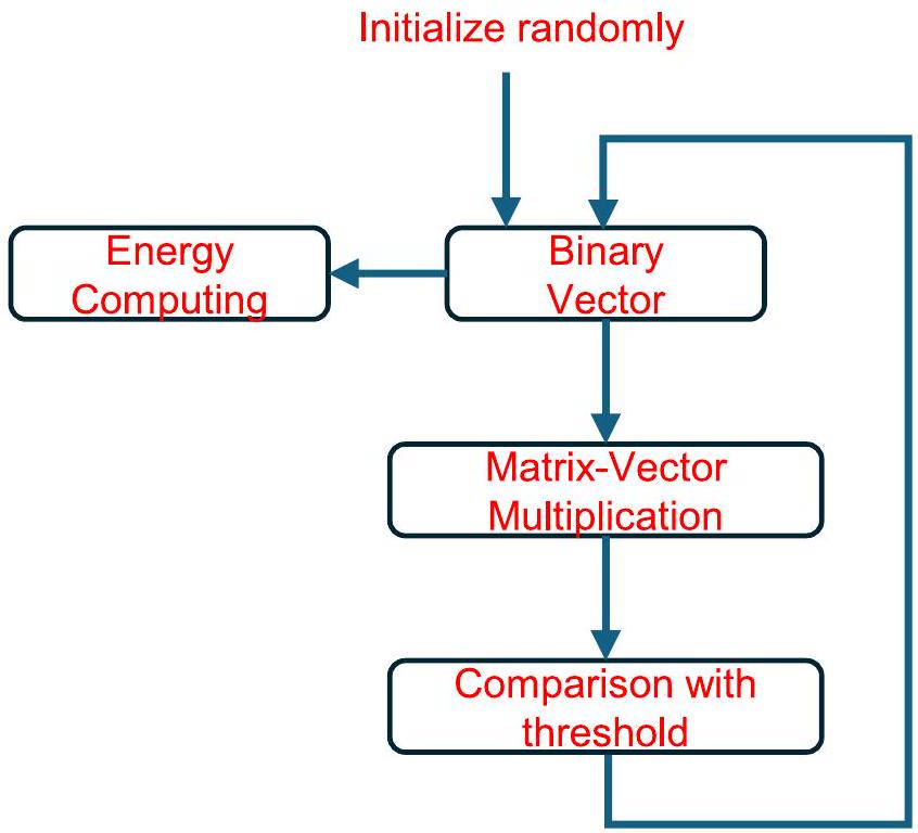
يمكن تنفيذ هذا الخوارزم في نظام حوسبة ضوئية مع بنية مصممة خصيصًا كما هو موضح في الشكل 1b. يمكن للدارات الضوئية أن تمثل هاملتونيان إيسينغ العشوائي الموضح في المعادلة (1). في خطوة الزمنيتم ترميز حالة الدوران في وحدة البيانات وإدخالها في وحدة وزن المصفوفة لإجراء عمليات MAC الخطية. في المستقبلات، يتم تطبيق عملية غير خطية بالإضافة إلى أنواع مختلفة من ضوضاء السعة على الإشارات لتنفيذ مقارنة عتبة غير خطية مكافئة.. يتم إرسال الناتج من المقارن بشكل متكرر كمتجه إدخال جديد في الخطوة إلى مجال MAC الخطي. يتقارب هذا الخوارزم المتكرر إلى توزيع الحالة الأساسية لنموذج إيسينغ المقابل، وبالتالي يجد الحد الأدنى من المعادلة (1) باحتمالية عالية.
المصفوفة المتكررة التي تضرب حالة الدوران الحالية هيوتم ربطه بنموذج إيسين المعني (انظر الطرق والمرجع 31). يعتمد الخوارزمية الموضحة في الشكل 1ب على حساب مصفوفة MAC التكراري، مما يشير إلى أن سرعة حساب عبء العمل الكامل تعتمد بشكل كبير على سرعة وزمن تأخير كل دورة MAC.
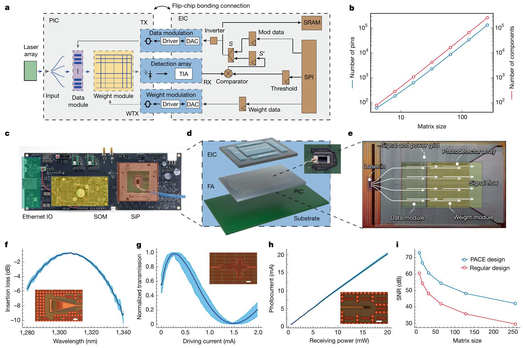
الشكل 2 | تنفيذ نظام PACE. أ، هيكل نظام PACE. الكتل الزرقاء تشير إلى مكونات المجال التناظري والكتل البنية تشير إلى مكونات المجال الرقمي. RX، المستقبل، بما في ذلك مضخم التوصيل (TIA) المتصل بأجهزة الكشف عن الضوء؛ TX، المرسل، بما في ذلك DAC ومحركات لمعدلات المتجهات؛ WTX، DAC الوزن ومحرك لمعدلات الوزن. ب، أعداد المكونات البصرية والمسامير مع زيادة حجم مصفوفة oMAC. ج، لوحة نظام PACE المتكاملة بحجم بطاقة PCle. SOM تعني النظام على الوحدة، متصلة مع PACE SiP من خلال SPI وجسر إلى الكمبيوتر المضيف عبر Ethernet IO. د، مخطط SiP المتقدم المعبأ مع ربط شريحة مقلوبة 2.5D. إدراج، SiP المعبأ مع توصيل الألياف وروابط الأسلاك إلى الركيزة. FA، مصفوفة الألياف. هـ، شرائح PIC مع تدفق الإشارة. المخطط. يتم توصيل مصادر الليزر الخارجية من خلال المنافذ المرفقة بالألياف وتدفقها عبر مجموعة المودولاتور المتجه. ثم يتم تعديل الإشارات الناتجة في وحدة الوزن وجمعها في مصفوفات المستقبل. يظهر الرسم العلوي طبقة إعادة توزيع الإشارة وشبكة الطاقة في المعادن في نهاية الخط. ف-ح، المكونات الوظيفية الحرجة وأدائها في PACE PIC، بما في ذلك موصل الشبكة (ف)، ومودولاتور ماخ-زيندر (ح) وكاشف الضوء Ge (ط). تمثل نقاط البيانات القيم المتوسطة لمواصفات الأجهزة في النظام. تشير المناطق المظللة إلى نطاقات الحد الأدنى والحد الأقصى. الصور المصغرة، صور مجهرية للأجهزة المقابلة. قضبان القياس، .أنا، نسبة الإشارة إلى الضوضاء مقابل حجم المصفوفة لنظام PACE مقابل التصميم العادي. التصميم العادي هو نفس النظام المبني على أساس الأجهزة الضوئية المبلغ عنها في المرجع 41.
لذلك، يمكن للحوسبة الضوئية تحقيق تحسين ملحوظ في الأداء في هذه المهام من خلال الاستفادة الفعالة من مزايا السرعة العالية في الحوسبة وانخفاض الكمون.
النظام والتنفيذ
لتنفيذ النظام الذي يمكنه تحقيق الأداء المستهدف باستخدام الخوارزمية التكرارية الاستدلالية الموصوفة أعلاه، هناك حاجة إلى دوائر ضوئية كبيرة الحجم يمكنها دعم حجم مصفوفة كبير بشكل ملحوظ، مع التحديات المتعلقة بعامل الشكل العالي للتكامل وأداء الجهاز المتسق. الشكل 2 يظهر التكامل العالي.محرك حسابات الحساب الضوئي (PACE) الذي طورناه في هذا العمل. كما هو موضح في الهيكل المعماري في الشكل 2أ، تم بناء هذا النظام لتنفيذ الخوارزمية التكرارية الاستدلالية الموضحة في القسم السابق بكفاءة. تم اختيار هيكل هجين مع دائرة متكاملة ضوئية (PIC) ودائرة متكاملة إلكترونية (EIC) مدمجة في نظام في حزمة (SiP)، حيثالبيانات البصرية وتنفذ وحدات الوزن عملية oMAC. تتعامل الدوائر التناظرية والرقمية المجاورة في EIC مع التحكم والمنطق التكراري. يتم تبادل الإشارات من خلال تحويل كهربائي إلى بصري عالي السرعة. التحويل بواسطة المودولات الضوئية والتحويل من الضوء إلى الكهرباء بواسطة كاشفات الضوء. تتولى الدوائر الرقمية في وحدة التحكم الإلكترونية معالجة إدخال البيانات، وقراءة البيانات، والعمليات المنطقية، بالإضافة إلى الساعة والتحكم. تم تصميم ذاكرة الوصول العشوائي الثابتة المدمجة (SRAM) لإدارة تخزين البيانات. المتجه الأولي، في إشارة إلى في الشكل 1ب، يتم حقن بيانات الوزن في محركات المتجهات ومحركات الوزن المقابلة من واجهة الأجهزة التسلسلية (SPI) لدفع معدلات المتجهات والأوزان. يتم إرسال قيم العتبة المحددة مسبقًا إلى المقارنات. ثم يبدأ النظام الدورات التكرارية. في تكرار مستقل، يتم إرسال نتائج المتجه المعالجة عبر القنوات الضوئية إلى المقارنات لتوليد متجه حالة جديد.، في إشارة إلى في الشكل 1ب. يتم تخزين المتجه الجديد والقيمة الذاتية المقابلة في SRAM بالإضافة إلى إعادته كمتجه ابتدائي لإعادة تشغيل معدلات المتجه في التكرار التالي. يتم إجراء ما مجموعه 5000 تكرار لضمان تقارب الحلول (انظر الطرق والبيانات الموسعة الشكل 1). لإقامة نظام oMAC بحجم مصفوفة أكبر من 64، يتطلب الأمر أكثر من 10,000 مكون بصري وأكثر من 10,000 دبوس لتوجيه الإشارات، كما هو موضح في الشكل 2b. وبالتالي، هناك حاجة إلى تكامل عالٍ مع تعبئة متقدمة. شكل تقليدي مع
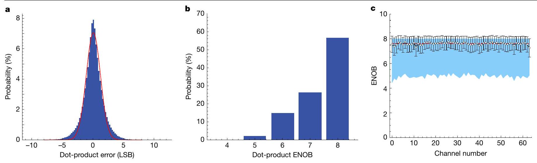
الشكل 3 | تحليل دقة ضرب المصفوفات البصرية. أ، توزيع دقة عملية ضرب النقطة الواحدة على 30,000 عملية ضرب نقطة عشوائية في تكوينين مختلفين لمصفوفة الوزن، مع إظهار متوسط خطأ قدره 0.06 LSB وانحراف معياري قدره 1.18 LSB. ب، هيستوغرام ENOB بين جميع أحداث ضرب النقاط العشوائية. ج، إحصائيات ENOB لكل قناة في دوائر PACE الضوئية. الخط الأحمر المتقطع يدل على متوسط 7.61 ENOB بين جميع القنوات. تشير أشرطة الخطأ إلى الانحراف المعياري والمنطقة المظللة تشير إلى نطاق الحد الأقصى والأدنى من ENOB في الاختبار. ستفشل المكونات البصرية الفردية والمكونات الكهربائية المتصلة من خلال لوحة منفصلة بسبب أحجام المكونات ومستوى كثافة التكامل، الذي يحده الحد الفيزيائي للتغليف في الفوتونيات المتكاملة.نظام PACE، الذي يستهدف شكل عامل متكامل للغاية، مبني على بطاقة بحجم PCle مع دمج PIC و EIC لتشكيل SiP. يتم التحكم في النظام الكامل من خلال SPI مع لوحة نظام على وحدة (SOM) ويتواصل مع المضيف عبر Ethernet IO (الشكل 2c). لتحقيق اتصالات الإشارة عالية الكثافة، يستخدم نظام PACE حلاً متقدماً للتغليف 2.5D مع ربط شريحة مقلوبة لتجميع PIC و EIC والركيزة كما هو موضح في الشكل 2d. يظهر الشكل الداخلي عرضًا علويًا لـ SiP مع الألياف المتصلة لربط PIC بالليزر الخارجي الذي يشغل الشريحة (انظر أيضًا الملاحظة التكميلية A لتفاصيل الدمج).
تم تصميم EIC على أساستكنولوجيا CMOS التجارية و PIC مبنية على أساس تجاريتكنولوجيا الفوتونيات السيليكونية مع دمج أكثر من 16,000 مكون فوتوني في شريحة واحدة، كما هو موضح في الشكل 2e. تم تصميم الدوائر الفوتونية في بنية ضوء غير متماسك مع سلسلة من وحدات البيانات، ووحدات الوزن، ومصفوفات المستقبلات، التي تم تنفيذها باستخدام معدلات ضوئية وكاشفات ضوئية.أربعة ليزر مستمر خارجي في مصفوفة متصلة بالدارات من مصفوفة الألياف المرفقة، من خلال موصلات شبكية عالية الأداء. تتراوح قوة التشغيل من أقل من مللي واط إلى حوالي 30 مللي واط لكل منها. قناة الليزر في النظام (انظر الملاحظة التكميلية أ). تصل كفاءة الاقتران المتوسطة إلى حوالي -1 ديسيبل عند طول موجي مركزي قريب منكما هو موضح في الشكل 2f.يتم إدخال المتجه الثنائي في مجموعة المودولاتور المتجه في الدائرة المتكاملة الضوئية من خلال المحولات الرقمية إلى التناظرية (DACs) والسائقين في الدائرة المتكاملة الإلكترونية لتحقيق الحالات الساطعة والداكنة في الإشارات الضوئية، والتي تت correspond إلى حالات 1 و 0 في المتجهات.
ثم يتم إرسال إشارات المتجهات المعدلة إلىوحدة وزن المصفوفة لمزيد من التعديل لتلبية ضرب المصفوفة-الناقل الخطي المعادل. يتم تعديل بيانات الناقل والوزن من خلال مجموعتين مختلفتين من معدلات ماخ-زيندر البصرية، مع طيف المعدل المستخرج النموذجي كما هو موضح في الشكل 2g. تتضمن مجموعة معدلات الناقل 64 وحدة متطابقة من معدلات ماخ-زيندر تعمل بتردد 1 جيجاهرتز مع أنظمة تعديل غير عائدة للصفر. (انظر الملاحظة التكميلية أ والشكل البياني الموسع 2 لجميع المعلومات الحيوية حول الأجهزة البصرية).
نظرًا لأن أوزان المصفوفة ثابتة لمشكلة إيسينغ معينة، تم تصميم وحدة تعديل الوزن بشكل مختلف عن مجموعة معدلات المتجهات. لتنفيذ وحدات الوزن القابلة لإعادة التكوين، تم تحسين معدلات الوزن للعمل بتردد أقل يبلغ 10 ميجاهرتز، بينما يتم تشغيلها بدقة بت أعلى بكثير بواسطة DACs والسائقين المجاورين. دقة التعديل المصممة correspondingly هي 8 بت. يتم تحويل وإدماج إشارات الضوء الناتجة في مصفوفات الكاشفات الضوئية وتضخيمها من خلال تحويل المقاومة.
الشكل 4 | نموذجين من إيزين مُهيئين في النظام. أ،حل مشكلة القص الأقصىمجموعة بيانات متجهة بحالتها الأولية العشوائيةحالة الحساب الوسيطة (ج) وحالة الحل النهائية (د). إدخالات، مُمَثلة ثنائي الأبعاد
المشكلة هي البحث عن الصورة المشفرة ذات حالات الطاقة الدنيا، مع حالتها الأولية العشوائية (f)، وحالة الحساب الوسيطة (g) وحالة الحل النهائية مع صورة حل ‘شبيهة بالقطط’ في حالة الأرض (h). الحواف التي تتطابق مع الولايات. e، Aالبحث عن التصوير المضغوط
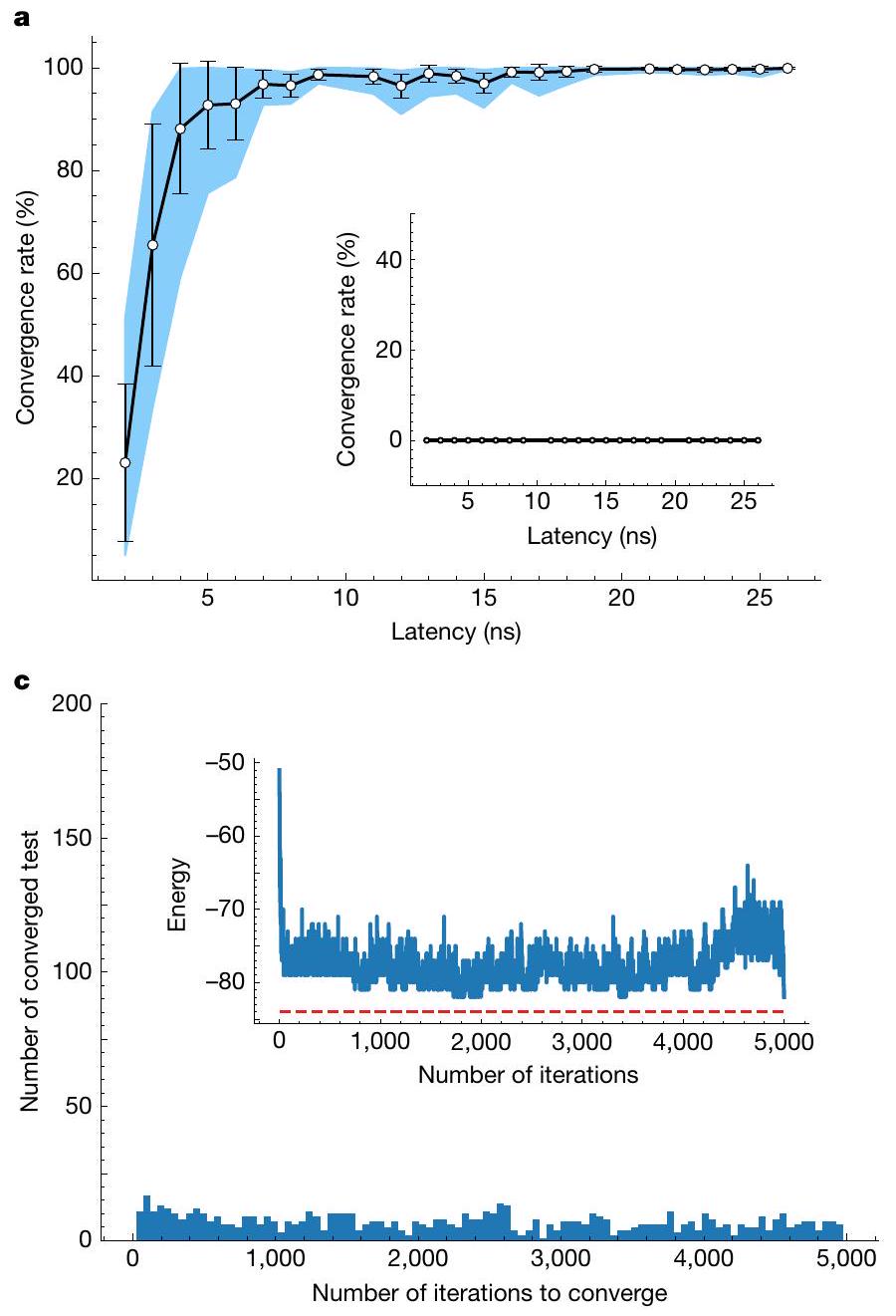
الشكل 5 | تقارب PACE Ising ومقارنته مع وحدة معالجة الرسوميات التجارية A10. أ، معدلات تقارب PACE Ising مقابل الكمون. تشير أشرطة الخطأ إلى الانحراف المعياري لعشر اختبارات عشوائية. في الإطار، عدم التقارب عندما تكون الإضاءة مطفأة في الدائرة، مما يدل على فعالية oMAC وأن الضوضاء الناتجة عن الأجهزة وحدها لا يمكن أن تحفز التقارب. ب، إحصائيات عدد التكرارات للوصول إلى الحل عند 5 نانوثانية من الكمون، على مدار 2000 حالة إدخال عشوائية. في الإطار، تطور الطاقة الدنيا في البحث التكراري. الخط الأحمر المتقطع يدل على الطاقة الدنيا المستهدفة. ج، إحصائيات عدد التكرارات التي تتقارب عند
زمن تأخير قدره 2 نانوثانية في نظام PACE. في الإطار، تطور الطاقة على مدى 5000 تكرار لحالة غير متقاربة. الخط الأحمر المتقطع يدل على الحد الأدنى المستهدف للطاقة. د، مقارنة عدد التكرارات للوصول إلى الحل بين نظام PACE وGPU التجاري. المتوسط هو 537 لنظام PACE و347 لـ NVIDIA A10 GPU، كما هو موضح بواسطة الخطوط المتقطعة. في الإطار، مقارنة زمن التأخير في الدورة الواحدة واستهلاك الوقت الكلي بين نظام PACE وNVIDIA A10 GPU. تم ضرب بيانات PACE في 100 للمقارنة البصرية.
لتنفيذ الهيكلية الاستدلالية بالكامل كما هو موضح في الخوارزمية، يحتاج نظام PACE إلى إدخال ضوضاء قابلة للتحكم في الدوائر لتحقيق تقلبات فعالة في البتات وبالتالي لتنفيذ بحث فعال عن الحل. توجد عدة مصادر للضوضاء القابلة للتحكم في نظامنا. تأتي الضوضاء المضافة بشكل أساسي من الليزر، والسائق التناظري، وTIA، بالإضافة إلى الضوضاء الرقمية المصممة في دوائر التحكم الرقمية. الضوضاء الناتجة عن الدوائر الضوئية أقل بكثير. لزيادة تقلبات البت المدفوعة بالضوضاء مع الحفاظ على توازن النظام الذي يؤدي إلى التقارب، يتم ضبط نسبة الإشارة إلى الضوضاء بنشاط من خلال قوة الليزر المدخلة، وتكوين كسب TIA المستقبل، وحقن الضوضاء الرقمية في المجال الرقمي.
دراسة دقة مصفوفة MAC البصرية
ثم نقوم بمعايرة النظام وتوصيف أداء النظام في ضرب المصفوفات الضوئية، وهو جوهر خوارزميتنا التقديرية (انظر الملاحظة التكميلية ب). للتحقق من أداء MAC في المجال الضوئي، يتم توصيف النظام من حيث دقة البت. توضح الشكل 3a توزيع خطأ الناتج النقطي المقاس لـ 30,000 متجه عشوائي تم حقنه في النظام في مجموعتان مختلفتان من تكوينات مصفوفة الوزن تتناسب مع عبء العمل الذي تم إثباته لدينا، دون أي ضبط نشط في الوقت الحقيقي لأوزان المصفوفة. متوسط خطأ قدره 0.06 بت الأقل أهمية (LSB) مع انحراف معياري يتم تحقيقه (لنتيجة أخرى لتكوينات الوزن العشوائية، انظر التوصيف الموسع في الملاحظة التكميلية C والشكل البياني الموسع 4). وبالمثل، تصل توزيع عدد البتات الفعالة (ENOB) إلى 8 بتات لأكثر من احتمالية وأكثر من 7 بتات للزيادة عنكما هو موضح في الشكل 3ب. الدقة بين القنوات المعروضة في الشكل 3ج تكشف أيضًا أن متوسط دقة قريب من 7.61 بت يتم تحقيقه في النظام تحت معدل بيانات 25 ميجاهرتز، دون أي تحكم نشط في التغذية الراجعة. يتم تطبيق معايرة أولية محددة للحفاظ على دقة النظام. النظام أيضًا متسامح معتقلبات درجة الحرارة مع انخفاض فعالية البت (انظر الملاحظة التكميلية ب). يمكن التخفيف من اعتماد درجة الحرارة المحيطة ومن المتوقع أن تتحسن دقة البت بشكل أكبر مع التحكم النشط في التغذية الراجعة ومراقبة النظام المنفذة.
عرض إيسينغ
يمكن حل مشاكل إيسينغ، التي تمثل مشاكل تحسين NP-complete النموذجية، بكفاءة باستخدام نظام PACE. للتحقق الكامل من مزايا الحوسبة الضوئية، كإثبات للمفهوم، نوضح بشكل خاص مشكلة قطع الرسم أو مشكلة التلوين الثنائي في هذا النظام النموذجي. يفصل نموذج إيسينغ/قطع الرسم الرؤوس إلى قسمين عن طريق تقليل عدد الحواف مع كل من أقسام الدوران لأعلى/أسفل (الموضحة كالرؤوس الصفراء/الزرقاء، على التوالي، في الشكل 4a) وزيادة عدد الحواف مع دورانات مختلفة (الموضحة كالرؤوس الرمادية في الشكل 4a). يعمل النظام لمدة 5000 تكرار قبل أن يتقارب إلى حل. يتم ضبط نسبة الإشارة إلى الضوضاء في النظام من خلال تكوينات مختلفة من طاقة الليزر وكسب TIA في المجال التناظري، بالإضافة إلى الضوضاء الرقمية في المجال الرقمي، للتقارب بكفاءة إلى حلولها مع الاستفادة من الضوضاء الديناميكية الداخلية لنظامنا. يتم توضيح الحالات الأولية والمتوسطة والنهائية النموذجية التي تتوافق مع الحد الأدنى من الحواف الملونة البالغ 9 في الشكل 4b-d. يمكن أن توفر الإضافات في الأشكال المرسومة ثنائي الأبعاد تصويرًا بصريًا بديهيًا للنسب النسبية للرؤوس الصفراء والزرقاء والرمادية داخل كل حالة. أيضًا، تم تصميم عرض مماثل لمشكلة تذكر الصورة المعادلة.في هذه الحالة، يمكن استخراج رسم بياني بحجم 64 مع 197 حافة من صورة RGB مسطحة بحجم -بكسل (الشكل 4e)، والتي تتوافق مع مصفوفة الجوار المتناظرة المنفية للرسم البياني. من خلال التطور الديناميكي عبر حالة أولية عشوائية، يتقارب نظام PACE أخيرًا إلى الحل الذي يتوافق مع الصورة المستهدفة التي تظهر قطة، كما هو موضح في الشكل 4h (انظر الطرق).
ثم نقوم بتوصيف أداء نظامنا في حل مشاكل إيسينغ (انظر الطرق، الملاحظة التكميلية A والشكل 5 من البيانات الموسعة). يتم ضبط ساعة النظام على 1 جيجاهرتز (انظر الملاحظة التكميلية A) ويمكن تكوين زمن التأخير في كل حلقة من 1 إلى 26 نانوثانية. يتم تسجيل النتائج من جميع التكرارات في ذاكرة النظام. مع عشرة دفعات من 2000 اختبار تقارب إيسينغ، فإن متوسط معدل التقارب للعثور على أفضل الحلول هو أكثر من مع أدنى زمن تأخير يبلغ 5 نانوثانية، كما هو موضح في الشكل 5a. ينخفض متوسط نسبة التقارب إلى أقل من عند زمن تأخير يبلغ 2 نانوثانية، بسبب القيود الداخلية للتأخير التي تفرضها دورات معالجة الإشارة بالإضافة إلى سرعة الساعة. يمكن رفع أو تحسين هذا القيد من خلال استخدام تصميم جهاز بديل مع عرض نطاق ترددي أعلى وسرعة ساعة أعلى مع تصميم دوائر أكثر إحكامًا في كل من EIC وPIC.يمكن أن يصل معدل التقارب إلى ما يقرب من مع إعداد زمن تأخير أكبر في النموذجين المعروضين. يشير ذلك إلى أن زمن حساب نظام PACE يمكن أن يحقق حدًا أدنى قدره 5 نانوثانية. هذا أسرع بنحو 500 مرة من تكرار واحد عند تشغيل نفس الحمل على وحدة معالجة الرسوميات التجارية عالية الأداء NVIDIA A10، والتي تم قياس زمن تأخير أكبر من .
يوضح الشكل 5b وc الرسوم البيانية لعدد التكرارات الإجمالية المطلوبة لتقارب إيسينغ في دفعة واحدة عند زمني تأخير 5 و2 نانوثانية، على التوالي.
مع مزيد من تحسين الإشارة والمعايرة، يمكن تحقيق زمن تأخير قدره 3 نانوثانية في الأجهزة المستقبلية. للمقارنة، قمنا أيضًا باستخراج الرسم البياني لحساب إيسينغ الذي يعمل على وحدة معالجة الرسوميات A10 باستخدام نفس الخوارزمية التكرارية الاستدلالية، حيث تمت إضافة الضوضاء في المجال الرقمي. ثم تتم مقارنة نتائج الأداء مع نظام PACE تحت تكوين زمن تأخير 5 نانوثانية، كما هو موضح في الشكل 5d. تظهر الرسوم البيانية تشابهًا قويًا، مع متوسط عدد التكرارات المطلوبة للتقارب البالغ 347 و537 لوحدة معالجة الرسوميات ونظام PACE، على التوالي. وبالمثل، يتم تحقيق إجمالي زمن حساب قدره مع نظام PACE، وهو أقصر بكثير من زمن الحساب مع وحدة معالجة الرسوميات، كما هو موضح في الإضافة في الشكل 5d. يعكس هذا تسريعًا بمقدار مرتبتين من حيث الحجم في نظام PACE مقارنة بوحدة معالجة الرسوميات (انظر الملاحظة التكميلية D والأشكال 6 و7 من البيانات الموسعة لمزيد من التفاصيل). يبرز هذا النتيجة ميزة الحوسبة الضوئية على زمن التأخير وسرعة الحساب التي حققها نظام PACE.
الخاتمة
في الختام، لقد قمنا بتنفيذ نظام مسرع ضوئي متكامل للغاية يعتمد على تقنية الفوتونيات السيليكونية التجارية. تم تحقيق دوائر MAC الضوئية مع أكثر من 16000 مكون مدمج على شريحة واحدة. تم تحقيق دقة متوسطة للبتات تبلغ 7.61 بت في النظام وتم عرض التطبيقات لحل مشكلة قطع الرسم مع زمن تأخير منخفض للغاية. تمت مقارنة الأداء لحل نفس عبء العمل الحسابي مع أداء وحدة معالجة الرسوميات A10 عالية الأداء التجارية. تكشف النتائج التجريبية أنه تم تحقيق تحسينات بأكثر من مرتبتين من حيث الحجم في زمن التأخير ووقت الحساب مع oMAC في نظام PACE مقارنة بوحدة معالجة الرسوميات التجارية. نعتقد أن هذا العرض يمكن أن يفيد استكشاف نماذج الحوسبة الجديدة، وهياكل الأنظمة، والتطبيقات المعتمدة على دوائر الفوتونيات المتكاملة على نطاق واسع.
المحتوى عبر الإنترنت
أي طرق، مراجع إضافية، ملخصات تقارير Nature Portfolio، بيانات المصدر، بيانات موسعة، معلومات تكميلية، شكر وتقدير، معلومات مراجعة الأقران؛ تفاصيل مساهمات المؤلفين والمصالح المتنافسة؛ وبيانات توفر البيانات والرموز متاحة على https://doi.org/10.1038/s41586-025-08786-6.
16. أشتيني، ف.، جيرز، أ. ج. وأفلاتوني، ف. شبكة عصبية ضوئية عميقة على الشريحة لتصنيف الصور. Nature 606، 501-506 (2022).
17. بسالتيس، د.، برادي، د.، غو، إكس.-ج. ولين، س. تصوير هولوجرافي في الشبكات العصبية الاصطناعية. Nature 343، 325-330 (1990).
18. سيو، س. ي. وآخرون. مراجعة لتقنية الفوتونيات السيليكونية وتطوير المنصات. J. Lightwave Technol. 39، 4374-4389 (2021).
19. ديلهاي، ب. وآخرون. توليد مشط التردد الضوئي من ميكرو ريزوناتور أحادي. Nature 450، 1214-1217 (2007).
20. بوغارتس، و. وآخرون. دوائر ضوئية قابلة للبرمجة. Nature 586، 207-216 (2020).
21. ليانغ، د. وباويرز، ج. إ. تقدم حديث في التكامل الضوئي الهجين III-V على السيليكون. Light Adv. Manuf. 2، 59-83 (2021).
22. وي، م. وآخرون. التكامل الأحادي للمواد القابلة للتغيير في الخط الخلفي في الفوتونيات السيليكونية المصنعة في المصانع. Nat. Commun. 15، 2786 (2024).
23. يانغ، ل.، جي، ر.، زانغ، ل.، دينغ، ج. وشي، كيو. معالج إشارة ضوئي متوافق مع CMOS على الشريحة. Opt. Express 20، 13560-13565 (2012).
24. تايت، أ. ن. وآخرون. شبكات ضوئية عصبية نيرومورفية باستخدام بنوك أوزان فوتونية سيليكونية. Sci. Rep. 7، 7430 (2017).
25. أندرسون، م.، ما، س.-ي.، وانغ، ت.، رايت، ل. وماكماهون، ب. محولات ضوئية. Trans. Mach. Learn. Res. (في الصحافة).
26. وانغ، ت. وآخرون. استشعار الصورة باستخدام شبكات عصبية ضوئية غير خطية متعددة الطبقات. Nat. Photonics 17، 408-415 (2023).
27. هيوز، ت. و.، مينكوف، م.، شي، ي. وفان، س. تدريب الشبكات العصبية الضوئية من خلال التراجع في الموقع وقياس التدرج. Optica 5، 864-871 (2018).
28. باي، س. وآخرون. التراجع في الموقع المحقق للتعلم العميق في الشبكات العصبية الضوئية. Science 380، 398-404 (2023).
29. زانغ، ه. وآخرون. شريحة عصبية ضوئية لتنفيذ شبكة عصبية ذات قيم معقدة. Nat. Commun. 12، 457 (2021).
30. تشينغ، ج. وآخرون. مجموعة صغيرة من الحلقات الدقيقة التي تؤدي إلى ضرب مصفوفة كبيرة ذات قيم معقدة. Front. Optoelectron. 15، 15 (2022).
31. روك-كارميس، س. وآخرون. خوارزميات تكرارية استدلالية لآلات إيسينغ الضوئية. Nat. Commun. 11، 249 (2020).
32. برابهو، م. وآخرون. تسريع آلات إيسينغ التكرارية في الدوائر الضوئية المتكاملة. Optica 7، 551-558 (2020).
33. أمبروجيو، س. وآخرون. شريحة analog-Al للتعرف على الكلام الفعال من حيث الطاقة والنقل. Nature 620، 768-775 (2023).
34. سكيب، م. وآخرون. في مؤتمر ومعرض اتصالات الألياف الضوئية 2022 (OFC) 01-03 (IEEE، 2022).
35. زو، ه. ه. وآخرون. حوسبة ضوئية فعالة من حيث المساحة مع شبكة عصبية متكاملة متباينة. Nat. Commun. 13، 1044 (2022).
36. جوبّي، ن. ب. وآخرون. في المؤتمر السنوي الرابع والأربعين حول معمارية الكمبيوتر (ISCA 17) 1-12 (ACM، 2017).
37. سيلو، د. وآخرون. في مؤتمر 2016 الحادي والعشرين للإلكترونيات الضوئية والاتصالات (OECC) الذي عقد بالتزامن مع المؤتمر الدولي 2016 حول الفوتونيات في التبديل (PS) 1-3 (IEEE، 2016).
38. بيريز، د. وكابماني، ج. تحليل قابل للتوسع لشبكات الموجات الضوئية المتكاملة العشوائية. أوبتيكا 6، 19-27 (2019).
39. ريد، ج. ت.، ماشانوفيتش، ج.، غاردس، ف. ي. وتومسون، د. ج. معدلات ضوئية من السيليكون. نات. فوتونيكس 4، 518-526 (2010).
40. فاسيك، ب. وكورتاس، إ. م. الترميز ومعالجة الإشارة لأنظمة التسجيل المغناطيسي (CRC، 2004).
41. فيرارو، ف. ج. وآخرون. منصات فوتونيات السيليكون من إيميك: نظرة عامة على الأداء وخارطة الطريق. في مؤتمر SPIE 12429، 1242909 (2023).
42. أميت، د. ج.، غوتفراوند، هـ. وسومبولينسكي، هـ. نماذج زجاج الدوران للشبكات العصبية. فيز. ريف. أ 32، 1007-1018 (1985).
43. شركة تايوان لصناعة أشباه الموصلات (TSMC). تقنية المنطق. TSMC https://www.tsmc.com/english/dedicatedFoundry/technology/logic (2024).
ملاحظة الناشر: تظل Springer Nature محايدة فيما يتعلق بالمطالبات القضائية في الخرائط المنشورة والارتباطات المؤسسية.
الوصول المفتوح: هذه المقالة مرخصة بموجب رخصة المشاع الإبداعي للاستخدام غير التجاري، والتي تسمح بأي استخدام غير تجاري، ومشاركة، وتوزيع، وإعادة إنتاج في أي وسيلة أو صيغة، طالما أنك تعطي الائتمان المناسب للمؤلفين الأصليين والمصدر، وتوفر رابطًا لرخصة المشاع الإبداعي، وتوضح إذا قمت بتعديل المادة المرخصة. ليس لديك إذن بموجب هذه الرخصة لمشاركة المواد المعدلة المشتقة من هذه المقالة أو أجزاء منها. الصور أو المواد الأخرى من طرف ثالث في هذه المقالة مشمولة في رخصة المشاع الإبداعي للمقالة، ما لم يُشار إلى خلاف ذلك في سطر الائتمان للمادة. إذا لم تكن المادة مشمولة في رخصة المشاع الإبداعي للمقالة واستخدامك المقصود غير مسموح به بموجب اللوائح القانونية أو يتجاوز الاستخدام المسموح به، ستحتاج إلى الحصول على إذن مباشرة من صاحب حقوق الطبع والنشر. لعرض نسخة من هذه الرخصة، قم بزيارة http:// creativecommons.org/licenses/by-nc-nd/4.0/.
(ج) المؤلفون 2025
طرق
مشكلة إيسينغ
الهاميلتونيان لمشكلة إيسينغ العامة يُعطى بواسطة
حيث أن يمثل عنصرًا من مصفوفة التي تصف الربط بين و . يُفترض أن تكون المصفوفة متناظرة، و يمثل المجال المغناطيسي الخارجي المطبق، والذي غالبًا ما يتم تجاهله لتقييم حلول إيسينغ. تتمثل مشكلة إيسينغ في العثور على متجه الدوران لتقليل .
في هذا العمل، نستخدم فئة من الخوارزميات التكرارية الاستدلالية التي تم اقتراحها كنهج فعال لحل مشاكل إيسينغ باستخدام الفوتونيات المتكاملة . في تنفيذ الأجهزة الضوئية، من الضروري تحويل متجه الدوران إلى متجه ثنائي ، حيث يتم تعريف كل عنصر على أنه . سيتم بدء هذا المتجه الثنائي عشوائيًا ثم يتم تكراره. تتضمن كل تكرار من الحلقة العمليات التالية:
في كل تكرار، يتم إجراء ضرب مصفوفة-متجه مشوش، يُشار إليه بـ
حيث أن مشتق من المصفوفة (المرجع 31). ثم يتم مقارنته مع متجه العتبة لإنتاج متجه الإدخال للتكرار التالي.
يتم حساب متجه العتبة مسبقًا، حيث يمكن وصف كل عنصر بأنه
تنفيذ عبء عمل إيسينغ
في مثال حفظ الصورة (صورة بكسل لقط)، قمنا بالتكرار على متجه ، بينما صورة القط هي صورة . تحتاج الصورة إلى أن تكون مسطحة إلى متجه ليتم تكرارها.
شرح التقارب
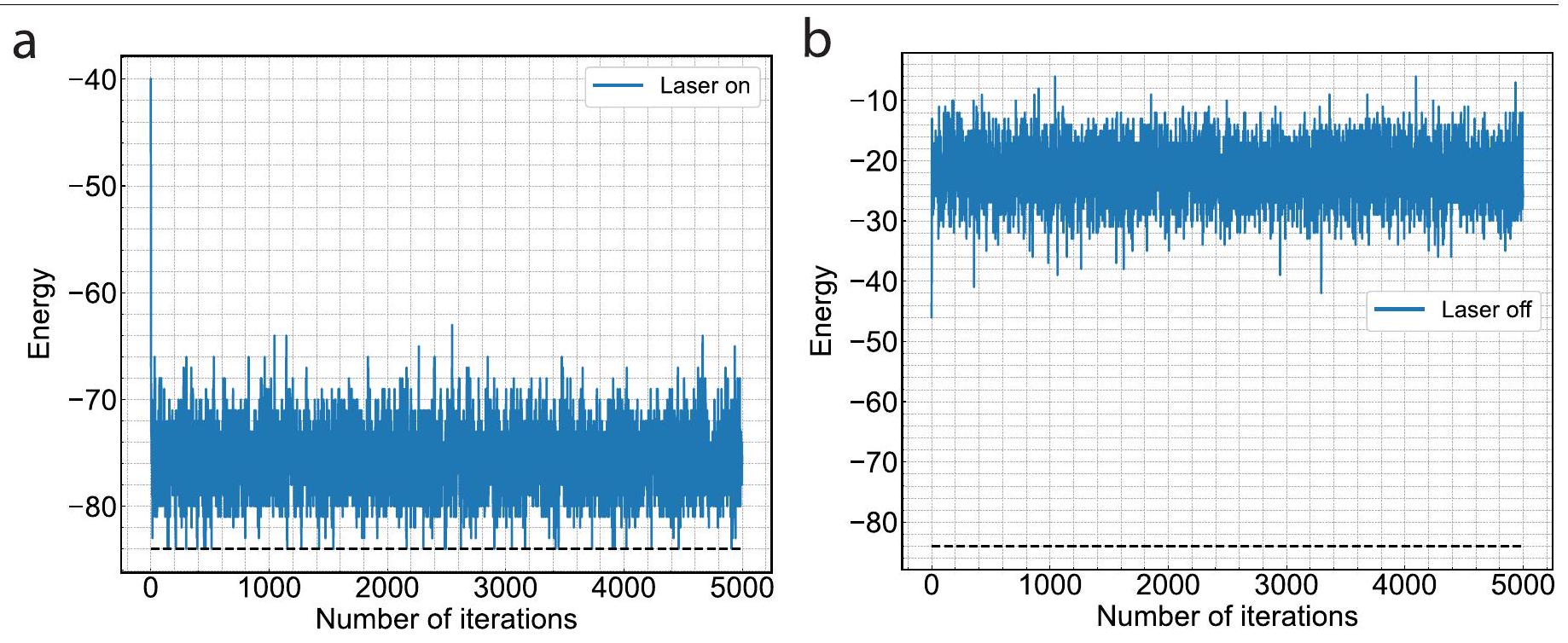
في تجارب عرض إيسينغ، يتم تكوين عدد التكرارات إلى 5000 ويتم تسجيل نتائج كل تكرار. عند اكتمال التكرارات، يتم حساب الطاقة المقابلة لكل نتيجة لتحديد ما إذا كان أي متجه قد وصل إلى حالة الطاقة الدنيا. إذا وصلت أي نتيجة إلى حالة الطاقة الدنيا، يُعتبر الحساب قد تقارب. تُظهر البيانات الموسعة الشكل 5 كل من الحالة المتقاربة (اللوحة أ) والحالة غير المتقاربة (اللوحة ب). بدأت كلتا الحالتين بمدخلاتهما العشوائية الخاصة وكانت طاقاتهما الأولية حوالي -40 . علاوة على ذلك، فإن القيمة النظرية للطاقة الدنيا، المشار إليها بالخط المنقط، هي -84 . من الواضح أن النظام يمكنه التكرار بسرعة نحو الحل الأمثل عندما يكون الليزر قيد التشغيل. على العكس، عندما يكون الليزر متوقفًا، تزداد الطاقة إلى حوالي -20 ، وهو أسوأ حتى من مدخل عشوائي.
عندما يتم إيقاف تشغيل الليزر، لا يتم توليد أي تيار ضوئي ويصبح ناتج النظام قريبًا من انحياز المحول التناظري إلى الرقمي 128، المتأثر بشكل رئيسي بالضوضاء من TIA. الانحراف المعياري لضوضاء TIA حوالي 2 LSB (أقل بتات ذات دلالة من المحول التناظري إلى الرقمي) لجميع القنوات. إذا تم ضبط عتبات المقارنات بعيدًا، على سبيل المثال، 6 LSB، قد تجد بعض القنوات صعوبة في تبديل مخرجاتها. سيؤدي ذلك إلى زيادة كبيرة في احتمال أن تكون هذه القنوات مدمجة مع 0s و 1s ثابتة أثناء التكرار. وبالتالي، يفشل النظام بأكمله في تحقيق التقارب.
توفر البيانات
تُقدم البيانات مع هذه الورقة. سيتم مراجعة جميع الطلبات الأخرى للبيانات والمواد بسرعة من قبل المؤلفين المعنيين لتحديد ما إذا كانت تخضع لالتزامات الملكية الفكرية أو السرية.
44. هرمكوفيتش، ج. خوارزميات لمشاكل صعبة. مقدمة في التحسين التوافقي، العشوائية، التقريب، والاستدلال (سبرينغر، 2001).
الشكر: نشكر س. زانغ وز. شيوي على دعمهما في هذا المشروع.
مساهمات المؤلفين: ي.س. و هـ.م. ابتكرا الفكرة. ي.س.، هـ.م. و م.س. صمما التجارب. س.هـ.، إ.د. و ز.س. نفذوا التجارب وعالجوا البيانات، بمساعدة ز.س.، ي.ب.، ج.ز.، ي.ز.، ي.إكس.، ج.-ك.ل.، ي.د.، هـ.ج.، ل.ج.، لي.و.، ل.أ.، ج.ز.، ج.س.، س.ي.، و.ز.، هـ.ز. و لو.و. و.ك.، س.هـ.، ل.أ. و ز.س. قدموا التحليل النظري. ي.س.، س.هـ. و ب.ب. كتبوا المخطوطة، مع مساهمات من جميع المؤلفين ودعم أكاديمي من ج.ر.-س. من خلال المشاركة في المناقشات النظرية ومراجعة المخطوطة. ي.س.، هـ.م. و ب.ب. أشرفوا على المشروع.
المصالح المتنافسة: لدى المؤلفين براءات اختراع ذات صلة مُنحت تحت أرقام براءات الاختراع الأمريكية B2 و US 11,907,832 B2.
معلومات إضافية
المعلومات التكميلية: النسخة عبر الإنترنت تحتوي على مواد تكميلية متاحة على https://doi.org/10.1038/s41586-025-08786-6.
يجب توجيه المراسلات والطلبات للحصول على المواد إلى بو بنغ، هواييو مينغ أو ييتشن شين.
معلومات مراجعة الأقران: تشكر ناتشر سايمون بيلودو، أنطوني ريزو والمراجعين الآخرين المجهولين على مساهمتهم في مراجعة الأقران لهذا العمل.
معلومات إعادة الطبع والأذونات متاحة على http://www.nature.com/reprints.
الشكل الموسع 1 | هيكل مضاعف المصفوفة-متجه PACE. تمثل الخطوط البرتقالية الإشارات الضوئية والخطوط السوداء المنقطة والصلبة تمثل الإشارة الكهربائية. تمثل الخطوط الصلبة أو المنقطة قبل دخول TIA زوجًا من الإشارات التفاضلية.
مقالة
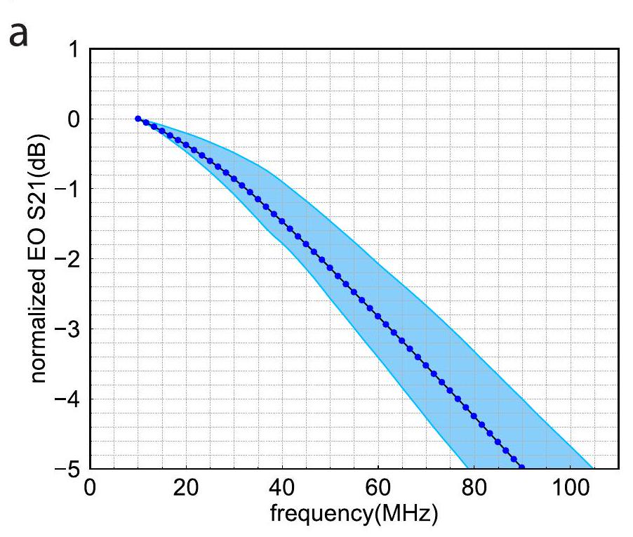
الشكل الموسع 2 | الاستجابة الكهربائية إلى الضوئية/الضوئية إلى الكهربائية للمعدل والكاشف الضوئي. أ، استجابة S21 لمعدل الوزن المستخدم في PIC. ب، استجابة S21 للكاشفات الضوئية المستخدمة
ب
في PIC. تمثل نقاط البيانات القيم المتوسطة لمواصفات الجهاز في النظام، وتوضح المناطق المظللة نطاقات الحد الأدنى والحد الأقصى.
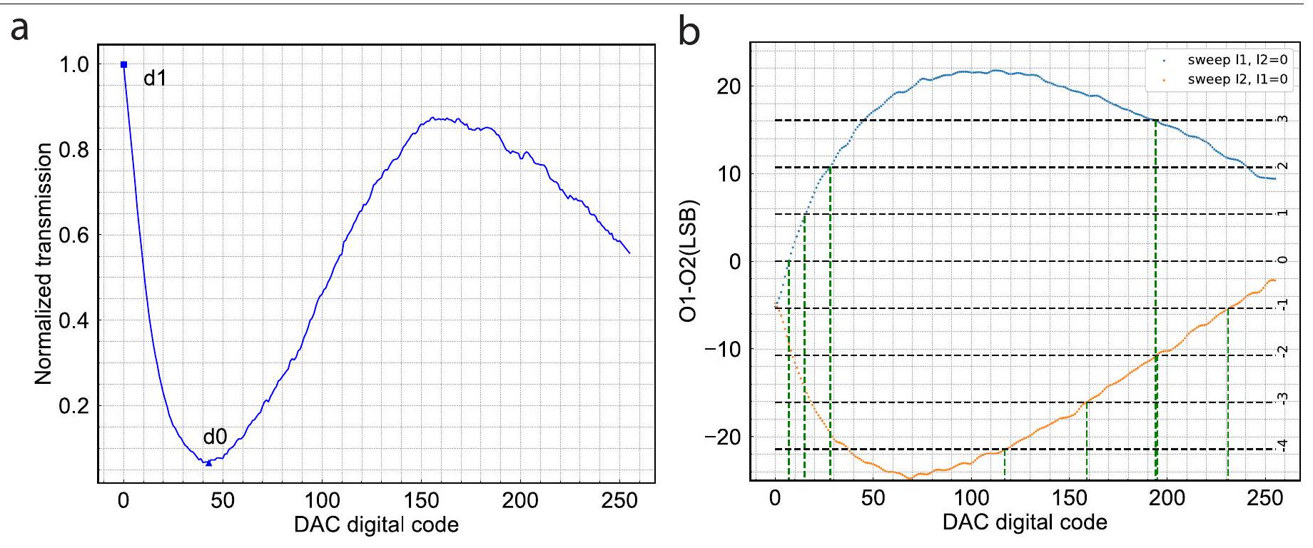
الشكل الموسع 3 | معايرة عنصر المتجه وعنصر المصفوفة. أ، منحنى النقل المنظم لشفرة DAC الرقمية التي تمسح لقناة عنصر المتجه. ب، منحنى منقى لعنصر المصفوفة وأيضًا الخريطة من القيمة العددية ( -4 إلى 3 ) إلى رموز DAC.
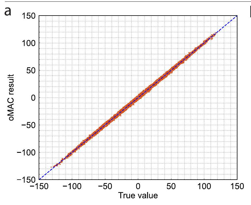
الشكل الموسع 4 | دقة ضرب المصفوفة-متجه. أ، نتائج oMAC مقابل القيم الحقيقية. الخط المنقط يتوافق مع الدالة ‘ والنقاط البرتقالية هي نتائج حساب oMAC. ، توزيع
عملية ضرب نقطة واحدة، والتي تظهر متوسط خطأ قدره -0.06 LSB وانحراف معياري قدره 1.37 LSB.
الشكل الموسع تغير الطاقة خلال التكرارات. أ، مثال على التقارب عندما يكون الليزر قيد التشغيل. ب، مثال على حالة غير متقاربة. الخط المتقطع يمثل حالة الطاقة المستهدفة. عندما يتم تحقيق الطاقة المستهدفة في غضون 5000 تكرار، يُعتبر ذلك تقاربًا.
أ
الشكل البياني الممتد 6 | سير عمل إيزينغ. أ، سير عمل نظام PACE، حيث يتم تصميم دائرة مخصصة لحساب الطاقة يمكن أن تعمل بالتوازي مع التكرارات. ب، سير عمل وحدة معالجة الرسوميات A10، حيث يتم تنفيذ التكرارات وحسابات الطاقة بشكل متسلسل.
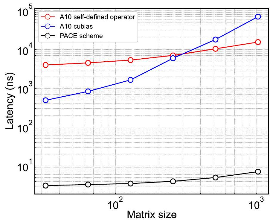
الشكل 7 من البيانات الموسعة | مقارنة الكمون بين وحدة معالجة الرسومات A10 ونظام PACE. الخط الأحمر يوضح الكمون للعمليات المعرفة ذاتياً، والتي تم تحسينها بناءً على العناصر المدرجة. الخط الأزرق هو الكمون عند استخدام مكتبة cuBLAS من NVIDIA. الخط الأسود هو الكمون المقدر باستخدام نظام PACE.
هو، ك.، زانغ، إكس.، رين، س. وسون، ج. في مؤتمر IEEE 2016 لرؤية الكمبيوتر والتعرف على الأنماط (CVPR) 770-778 (IEEE، 2016).
كريزيفسكي، أ.، سوتسكيڤر، إ. وهينتون، ج. تصنيف ImageNet باستخدام الشبكات العصبية التلافيفية العميقة. تقدمات في نظم معالجة المعلومات العصبية 25 (NIPS 2012) 1-9 (2012).
شين، ي. وآخرون. التعلم العميق مع الدوائر النانوية المتماسكة. نات. فوتونيكس 11، 441-446 (2017).
Lin، X. وآخرون. التعلم الآلي الكلي البصري باستخدام الشبكات العصبية العميقة الانكسارية. العلوم 361، 1004-1008 (2018).
Shiyue Hua , Erwan Divita , Shanshan Yu , Bo Peng , Charles Roques-Carmes , Zhan Su , Zhang Chen , Yanfei Bai , Jinghui Zou , Yunpeng Zhu , Yelong Xu , Cheng-kuan Lu , Yuemiao Di , Hui Chen , Lushan Jiang , Lijie Wang , Longwu Ou , Chaohong Zhang , Junjie Chen , Wen Zhang , Hongyan Zhu , Weijun Kuang , Long Wang , Huaiyu Meng , Maurice Steinman & Yichen Shen
Integrated photonics, particularly silicon photonics, have emerged as cutting-edge technology driven by promising applications such as short-reach communications, autonomous driving, biosensing and photonic computing .As advances in AI lead to growing computing demands, photonic computing has gained considerable attention as an appealing candidate. Nonetheless, there are substantial technical challenges in the scaling up of integrated photonics systems to realize these advantages, such as ensuring consistent performance gains in upscaled integrated device clusters, establishing standard designs and verification processes for complex circuits, as well as packaging large-scale systems. These obstacles arise primarily because of the relative immaturity of integrated photonics manufacturing and the scarcity of advanced packaging solutions involving photonics. Here we report a large-scale integrated photonic accelerator comprising more than 16,000 photonic components. The accelerator is designed to deliver standard linear matrix multiply-accumulate (MAC) functions, enabling computing with high speed up to 1 GHz frequency and low latency as small as 3 ns per cycle. Logic, memory and control functions that support photonic matrix MAC operations were designed into a cointegrated electronics chip. To seamlessly integrate the electronics and photonics chips at the commercial scale, we have made use of an innovative 2.5D hybrid advanced packaging approach. Through the development of this accelerator system, we demonstrate an ultralow computation latency for heuristic solvers of computationally hard Ising problems whose performance greatly relies on the computing latency.
In recent years, the advent of new computing models has instigated notable advancements in computational technology. These technologies are primarily dedicated to accelerating linear computation. Specifically, matrix MAC operations play a pivotal role in deep learning and neural networks . They form the core of numerous machine learning algorithms and account for most computational resources required for training and inference. However, MAC operations are power-intensive, exacerbating power consumption and operational requirements of transistors. This situation is worsened by the increasing complexity of computation models and the growing need for real-time processing. Driven by the conflict between the limitation of digital semiconductor techniques and the strong demand for higher performance, alternative computing platforms have been proposed, such as photonic computing, shifting from traditional electronic computing . This transformation, although still in its nascent stages, presents a promising solution to challenges posed by the growing demand for high-speed, low-latency data processing . The advantage of photonic computation derives from the unique properties of light, allowing
simultaneous multiplication and accumulation processes as optical signals travel through guided-wave circuits. Such massive parallel operations substantially reduce data movement, thereby conserving energy. Furthermore, light-based devices can avoid the resistive losses and heating issues encountered by their electronic counterparts, potentially enhancing their energy efficiency .
However, even though the concept of optical computing was introduced several decades , a resurgence of interest has recently been spurred by rapid progress and recent innovations in silicon photonics, nanophotonics and materials science . A variety of technical developments in integrated photonics has demonstrated their potential for accelerating computation . These efforts, complemented by promising results on optical transformers and nonlinear activation functions, have confirmed the extensive potential of photonics as a platform for multitask, high-performance computing . Recent studies have also shown that integrated silicon photonics can perform training tasks . Moreover, photonic computing has demonstrated its potential to solve complex problems more efficiently .
Fig.1| Latency comparison and principle of the heuristic recurrent algorithm. a, Comparison of latency between oMAC and TPU systolic array, a typical enhanced MAC operation. In the TPU, we assume that the clock frequency is and the latency accumulates by orders of magnitude with the increase of clock cycles and matrix size linearly. By contrast,
the latency only increases linearly with the expanding matrix size in oMAC owing to the change of path length, limited to nanoseconds.b, Principle of the heuristic recurrent algorithm for oMAC. denotes the current data vector and denotes the weight module representing the transition probability.
Although new optical materials, architectures and strategies have been introduced to photonic computing to improve either their performance or their throughput, these demonstrations have been limited to single components or small-scale circuits. The real potential of photonic computing lies in very-large-scale integration and volume manufacturing technologies that could overturn or add value to traditional computing architectures. Such advantages are yet to be demonstrated in hardware, with several critical challenges still to be addressed. First, with the absence of storage in the optical domain, photonic computing must rely on optical-electronic cointegration and conversion of signals from one domain to the other. Second, like other technologies such as computing in memory , photonic computing operates in the analogue domain, which means that it faces challenges in computation accuracy, especially for large, complex circuits. Third, photonic computing requires the development of compatible models and algorithms to be implemented on this new form of hardware.
In this paper, we present experimental results showing a marked advancement in highly integrated photonic computing technologythe development of an optical matrix-vector computing acceleration chip that integrates more than 16,000 photonic components with advanced packaging. Performance analyses of this system indicate its potential for high throughput and, especially, low latency, surpassing traditional electronic-based solutions in terms of latency by two orders of magnitude. Our system design directly addresses the three above-mentioned challenges and illustrates the possibilities of using light for computation on large scales, representing an important milestone in photonic computing commercialization.
Optical MAC for heuristic recurrent algorithm
As an analogue computing approach, photonic computing has the potential advantage of achieving high bandwidth, high energy efficiency and low latency. High-bandwidth photonic computing relies on high-speed optical signal processing that can reach more than 100 Gbps (ref. 34). Energy efficiency can be further improved in architectures making use of wavelength multiplexing and/or new material platforms . However, realizing latency speedups is technically very challenging, as they rely on large-scale optical vectors and matrices to avoid time penalty from matrix decomposition or multicycle analogue-to-digital conversions. In a digital MAC operation, such as systolic arrays in tensor processing units (TPUs) , dot-product operations are decoupled and operate through the matrix elementwise (Fig. 1a, inset). Although the energy consumption can be greatly reduced by
limiting short-reach data transfer between neighbouring units, the latency grows substantially as the matrix size expands, as shown by the red curve in Fig. 1a. By contrast, latency in photonic circuits is only limited by the optical path length, which scales linearly with matrix size. Latency can therefore be smaller than 10 ns or limited by a small amount of clock cycles, which remain negligible compared with latency in digital circuits, even for large matrix sizes (approximately 50). The growth factor of optical MAC (oMAC) latency is only several picoseconds, which is close to one-thousandth of TPUs (see Supplementary Note A and Extended Data Fig. 1). This contrast highlights the potential of scaled-up photonic accelerators for applications that require large throughput and ultralow latency.
Relying on large throughput and low latency, large-scale photonic computing systems are an ideal platform to implement heuristic algorithms for combinatorial optimization tailored for photonic platforms, such as photonic recurrent Ising samplers . Here we focus on solving combinatorial problems that can be cast into an arbitrary quadratic Hamiltonian form:
in which denotes an matrix and . This Hamiltonian is that of an Ising model , which equivalently describes the interaction of many particles in terms of the coupling matrix and spin states or normalized spin states , with .
This algorithm can be implemented in a photonic computing system with a specifically designed architecture as shown in Fig. 1b. The photonic circuits can map the arbitrary Ising Hamiltonians described in equation (1). At time step , the spin state is encoded in the data module and fed into the matrix weight module for linear MAC operations. At the receivers, a nonlinear operation as well as various types of amplitude noise are imparted to the signals to implement an equivalent nonlinear threshold comparison . The output from the comparator is recurrently sent back as the new input vector at step to the linear MAC domain. This recurrent algorithm converges to the ground-state distribution of the corresponding Ising model, therefore finding the minima of equation (1) with high probability.
The recurrent matrix that is multiplying the current spin state is and is mapped to the Ising model of interest (see Methods and ref. 31). The algorithm shown in Fig. 1b relies on iterative matrix MAC computation, indicating that the computation speed of the full workload depends heavily on the speed and latency of each MAC cycle.
Fig. 2 | PACE system implementation. a, PACE system architecture. Blue blocks indicate analogue domain components and brown blocks indicate digital domain components. RX, receiver, including transimpedance amplifier (TIA) connecting to the photodetectors; TX, transmitter, including DAC and drivers for the vector modulators; WTX, weight DAC and driver for the weight modulators. b, Numbers of optical components and pins as the oMAC matrix scales up. c, Integrated PACE system board in PCle-card-size form factor. SOM stands for system on module, connecting with PACE SiP through the SPI and bridging to the host computer through Ethernet IO. d, Diagram of the advanced packaged SiP with 2.5D flip-chip bonding. Inset, packaged SiP with fibre attach and wire bonds to the substrate. FA, fibre array. e, PIC chips with signal flow
diagram. External laser sources are coupled through the fibre-attached ports and flow through the vector modulator array. The resulting signals are then modulated in the weight module and collected at the receiver arrays. The top trace shows the signal redistribution layer and power grid at the back-end-ofline metals.f-h, Critical functional components and their performance in the PACE PIC, including grating coupler (f), Mach-Zehnder modulator (g) and Ge photodetector (h). The data points represent the mean values of device specs in the system. Shaded areas denote the min-max ranges. Insets, microscope images of the corresponding devices. Scale bars, .i, SNR versus matrix size for the PACE system versus regular design. Regular design is the same system built on the basis of photonic devices reported in ref. 41 .
Therefore, photonic computing can achieve marked performance improvement in these tasks by effectively using the advantages of high computing speed and low latency.
System and implementation
To implement the system that can achieve the target performance running the above-described heuristic recurrent algorithm, large-scale photonic circuits that can support considerably large matrix size are necessary, with the challenges of high integration form factor and consistent device performance. Figure 2 shows the highly integrated Photonic Arithmetic Computing Engine (PACE) that we developed in this work. As shown in the architecture in Fig. 2a, this system is built to efficiently implement the heuristic recurrent algorithm described in the previous section. A hybrid architecture is chosen with a photonic integrated circuit (PIC) and an electronic integrated circuit (EIC) integrated in a system in package (SiP), in which optical data and weight modules execute the oMAC operation. Adjacent analogue and digital circuits in the EIC handle control and iterative logics. Signals are exchanged through a high-speed electrical-to-optical
conversion by optical modulators and optical-to-electrical conversion by photodetectors. The digital circuits in the EIC handle the data feed-in, read-out and logic operations, as well as the clock and control. An embedded static random-access memory (SRAM) is designed to manage data storage. The initial vector , referring to in Fig. 1b, and weight data are injected into the corresponding vector drivers and weight drivers from the Serial Peripheral Interface (SPI) bus to drive the vector and weight modulators. The preset threshold values are sent to the comparators. The system then starts the iterative cycles. In a standalone iteration, processed vector results through the photonic channels are sent to the comparators to generate a new state vector , referring to in Fig. 1b. The new vector and the corresponding eigenvalue are stored in the SRAM as well as being sent back as the starting vector to re-drive the vector modulators in the next iteration. A total of 5,000 iterations is performed to guarantee the convergence of the solutions (see Methods and Extended Data Fig. 1).
To establish an oMAC system with matrix size larger than 64 , more than 10,000 optical components and more than 10,000 pins to route signals are required, as shown in Fig. 2b. Thus, high integration with advanced packaging is required. A traditional form factor with
Fig.3|Optical matrix multiplication accuracy analysis. a, Distribution of single dot-product operation accuracy over 30,000 random vector dot-product operations in two different weight matrix configurations, showing an average error of 0.06 LSB and standard deviation of 1.18 LSB.b, Histogram of ENOB
among all random dot-product events. c, The channel-by-channel ENOB statistics in the PACE photonic circuits. The dashed red line denotes an average of 7.61 ENOB among all channels. The error bars denote the standard deviation and the shaded area denotes the range of the maximum and minimum ENOB in the test.
individual optical components and electrical components connected through a separate board would fail owing to component sizes and the level of integration density, which is limited by the physical limit of packaging in integrated photonics . The PACE system, targeting highly integrated form factor, is built on a PCle-size card with integration of the PIC and the EIC to form the SiP. The full system is controlled through the SPI with a system on module (SOM) board and communicates with the host through Ethernet IO (Fig. 2c). To achieve the high-density signal connections, the PACE system uses a 2.5D advanced packaging solution with flip-chip bonding to assemble the PIC, EIC and the substrate as shown in Fig. 2d. The inset shows a top view of the SiP with the fibre attach to connect the PIC with external laser that drives the chip (also see Supplementary Note A for integration details).
The EIC is designed on the basis of a commercial CMOS technology and the PIC is built on a commercial silicon photonics technology with integration of more than 16,000 photonics components in a single chip, as illustrated in Fig. 2e. The photonic circuits are designed in an incoherent light architecture with series of data modules, weight modules and receiver arrays, which are implemented with optical modulators and photodetectors . Four external continuous-wave lasers in an array are coupled into the circuits from the attached fibre array, through high-performance grating couplers. The operating power ranges from sub-mW to about 30 mW for each
laser channel in the system (see Supplementary Note A). The average coupling efficiency reaches about -1 dB at a central wavelength near , as shown in Fig. 2f. A binary vector is fed into the vector modulator array in the PIC through the digital-to-analogue converters (DACs) and drivers in the EIC to achieve the bright and dark states in optical signals, corresponding to the 1 and 0 states in the vectors.
The modulated vector signals are then sent to a matrix weight module for further modulation to fulfil the equivalent linear matrix-vector multiplication. The vector and weight data are modulated through two different sets of optical Mach-Zehnder modulators, with typical extracted modulator spectra as shown in Fig. 2g. The vector modulator array includes 64 identical units of Mach-Zehnder modulators operating at 1 GHz with non-return-to-zero modulation schemes (see Supplementary Note A and Extended Data Fig. 2 for all critical optical device information).
Because the matrix weights are fixed for a given Ising problem, the weight modulator module is designed differently from the vector modulator array. To implement the reconfigurable weight units, the weight modulators are optimized to operate at a lower frequency of 10 MHz , while being driven with much higher bit resolution by adjacent DACs and drivers. The correspondingly designed modulation accuracy is 8 bits. The output optical signals are converted and merged at the photodetector arrays and amplified through transimpedance
Fig. 4 | Two Ising models configured in the system. a, A max-cut problem-solving a vector dataset with its random initial state , intermediate computation state (c) and final solution state (d). Insets, 2D-mapped
problem, to search for the encoded image with the minimum energy states, with its random initial state (f), intermediate computation state (g) and final solution state with a’cat-like’ ground-state solution image (h).
edges that match with the states. e, A squeezed imaging-searching
Fig.5|PACE Ising convergence and its comparison with a commercial A10 GPU. a, PACE Ising convergence rates versus latency. The error bars denote the standard deviation of ten random tests. Inset, non-convergence when the light is off in the circuit, indicating the effectiveness of oMAC and that pure hardware noise alone cannot induce convergence. b, Statistics of the number of iterations to solution at 5 ns latency, over 2,000 random input states. Inset, minima energy evolution in the iterative search. Dashed red line denotes the target minima energy.c, Statistics of the number of iterations that converge at
2 ns latency in the PACE system. Inset, energy evolution over 5,000 iterations for an unconverged case. Dash red line denotes the target minima energy. d, Comparison of the number of iterations to solution between the PACE system and the commercial GPU. The average counts are 537 for the PACE system and 347 for the NVIDIA A10 GPU, shown by dashed lines. Inset, comparison of single cycle latency and total time consumption between the PACE system and the NVIDIA A10 GPU. PACE data are multiplied by 100 for visual comparison.
To fully implement the heuristic architecture as explained in the algorithm, the PACE system needs to introduce controllable noises in the circuits to achieve efficient bit flips and hence to implement an effective search of the solution. Several sources of controllable noise are present in our system. The added noise primarily comes from the laser, analogue driver, TIA, as well as digital noise designed in the digital control circuits. The noise generated from the photonic circuits is considerably smaller. To increase the noise-driven bit flipping while maintaining the balance of the system that leads to convergence, the SNR is actively tuned by the input laser power, receiver TIA gain configuration and digital noise injection in the digital domain.
Optical matrix MAC accuracy study
We then calibrate the system and characterize the performance of the system on optical matrix multiplication, which is the core of our heuristic algorithm (see Supplementary Note B). To verify the MAC performance in the photonic domain, the system is characterized in terms of bit accuracy. Figure 3a shows a measured dot-product error distribution for 30,000 random vectors injected into the system in
two different sets of weight matrix configurations that match our demonstrated workload, without any real-time active feedback tuning of the weights. An average error of 0.06 least significant bits (LSB) with standard deviation is achieved (for another result for randomized weight configurations, see expended characterization in Supplementary Note C and Extended Data Fig. 4). Correspondingly, the effective number of bits (ENOB) distribution reaches 8 bits for more than probability and more than 7 bits for greater than , as shown in Fig. 3b. The channel-to-channel bit accuracy presented in Fig. 3c also reveals that an average of close to 7.61-bit accuracy is achieved in the system under 25 MHz data rate, without any active feedback control. A specific preliminary calibration is applied to maintain the system accuracy. The system is also tolerant to temperature fluctuation with downgrade of an effective bit (see Supplementary Note B). The ambient temperature dependence can be mitigated and the bit accuracy is expected to be further improved with active feedback control and monitoring of the system implemented.
Ising demonstration
Ising problems, which represent typical NP-complete optimization problems, can be solved efficiently with the PACE system. To fully verify the advantages of photonic computing, as a proof of concept, we specifically demonstrate a graph max-cut or two-colouring problem in this prototype system. The Ising model/max-cut separates vertices into two partitions by minimizing the number of edges with each of the spin up/ down partitions (shown as yellow/blue vertices, respectively, in Fig. 4a) and maximizing the number of edges with different spins (shown as grey vertices in Fig. 4a). The system runs for 5,000 iterations before converging to a solution. The system SNR is tuned through different configurations of laser power and TIA gain in the analogue domain, as well as digital noise in the digital domain, to efficiently converge to its solutions while making use of the intrinsic dynamic noise of our system. The typical initial, intermediate and final states corresponding to a minimum coloured edge of 9 are illustrated in Fig. 4b-d. The insets of the 2D-mapped figures can provide an intuitive visual depiction of the relative proportions of yellow, blue and grey vertices within each state. Also, a similar demonstration is designed for an equivalent image memorization problem . In this case, a 64 -size graph with 197 edges can be extracted from a flattened -pixel RGB image (Fig. 4e), corresponding to the graph’s negated symmetrized adjacency matrix. Evolving dynamically through a random initial state, the PACE system finally converges to the solution corresponding to the target image showing a cat, as shown in Fig. 4h (see Methods).
We then characterize the performance of our system in solving Ising problems (see Methods, Supplementary Note A and Extended Data Fig. 5). The system clock is set at 1 GHz (see Supplementary Note A) and the latency in each loop can be configured from 1 to 26 ns . The results from all iterations are recorded in the system memory. With ten batches of 2,000 Ising convergence tests, the average convergence rate to find the best solutions is more than with a lowest latency of 5 ns , as shown in Fig. 5a. The average convergence ratio decreases to less than at a latency of 2 ns , owing to the intrinsic delay limitations introduced by signal processing cycles as well as the clock speed. The limitation can be lifted or improved by using alternative device design with higher bandwidth and higher clock speed of operation with tighter circuits design in both the EIC and the PIC . The convergence rate can reach nearly with a larger latency setting in the two demonstrated models. It indicates that the computation latency of the PACE system can achieve a minimum of 5 ns . This is nearly 500 times faster than a single iteration when running the same workload on a commercial high-end NVIDIA A10 GPU, for which greater than latency is measured.
Figure 5b,c shows histograms of the total iteration counts required for Ising convergence in one batch at latencies of 5 and 2 ns, respectively.
With further signal and calibration improvement, a latency of 3 ns could be realized in future devices. For comparison, we also extracted the histogram of the Ising calculation running on a A10 GPU using the same heuristic recurrent algorithm, in which noise is added in the digital domain. The performance results are then compared with the PACE system under 5 ns latency configuration, as shown in Fig. 5d. The histograms exhibit strong similarity, with average numbers of iterations required for convergence of 347 and 537 for the GPU and the PACE system, respectively. Correspondingly, a total computation time of is realized with the PACE system, much shorter than the computation time with the GPU, as shown in the inset of Fig. 5d. This reflects a two-orders-of-magnitude acceleration in the PACE system compared with the GPU (see Supplementary Note D and Extended Data Figs. 6 and 7 for more details). This result highlights the advantage of photonic computing on latency and computation speed realized by the PACE system.
Conclusion
In conclusion, we have successfully implemented a highly integrated photonic accelerator system based on commercial silicon photonics technology. The photonics MAC circuits are realized with more than 16,000 components integrated on a single chip. An average bit accuracy of 7.61 bits is achieved in the system and applications for solving the max-cut problem with ultralow latency are demonstrated. The performance to solve the same computation workload is compared with that of a commercial high-performance A10 GPU. The experimental results reveal that more than two-orders-of-magnitude improvements in latency and computing time are achieved with oMAC in the PACE system compared with the commercial GPU. We believe that this demonstration could benefit the exploration of new computing models, system architectures and applications based on large-scale integrated photonics circuits.
Online content
Any methods, additional references, Nature Portfolio reporting summaries, source data, extended data, supplementary information, acknowledgements, peer review information; details of author contributions and competing interests; and statements of data and code availability are available at https://doi.org/10.1038/s41586-025-08786-6.
16. Ashtiani, F., Geers, A. J. & Aflatouni, F. An on-chip photonic deep neural network for image classification. Nature 606, 501-506 (2022).
17. Psaltis, D., Brady, D., Gu, X.-G. & Lin, S. Holography in artificial neural networks. Nature 343, 325-330 (1990).
18. Siew, S. Y. et al. Review of silicon photonics technology and platform development. J. Lightwave Technol. 39, 4374-4389 (2021).
19. Del’Haye, P. et al. Optical frequency comb generation from a monolithic microresonator. Nature 450, 1214-1217 (2007).
20. Bogaerts, W. et al. Programmable photonic circuits. Nature 586, 207-216 (2020).
21. Liang, D. & Bowers, J. E. Recent progress in heterogeneous III-V-on-silicon photonic integration. Light Adv. Manuf. 2, 59-83 (2021).
22. Wei, M. et al. Monolithic back-end-of-line integration of phase change materials into foundry-manufactured silicon photonics. Nat. Commun. 15, 2786 (2024).
23. Yang, L., Ji, R., Zhang, L., Ding, J. & Xu, Q. On-chip CMOS-compatible optical signal processor. Opt. Express 20, 13560-13565 (2012).
24. Tait, A. N. et al. Neuromorphic photonic networks using silicon photonic weight banks. Sci. Rep. 7, 7430 (2017).
25. Anderson, M., Ma, S.-Y., Wang, T., Wright, L. & McMahon, P. Optical transformers. Trans. Mach. Learn. Res. (in the press).
26. Wang, T. et al. Image sensing with multilayer nonlinear optical neural networks. Nat. Photonics 17, 408-415 (2023).
27. Hughes, T. W., Minkov, M., Shi, Y. & Fan, S. Training of photonic neural networks through in situ backpropagation and gradient measurement. Optica 5, 864-871 (2018).
28. Pai, S. et al. Experimentally realized in situ backpropagation for deep learning in photonic neural networks. Science 380, 398-404 (2023).
29. Zhang, H. et al. An optical neural chip for implementing complex-valued neural network. Nat. Commun. 12, 457 (2021).
30. Cheng, J. et al. A small microring array that performs large complex-valued matrix-vector multiplication. Front. Optoelectron. 15, 15 (2022).
31. Roques-Carmes, C. et al. Heuristic recurrent algorithms for photonic Ising machines. Nat. Commun. 11, 249 (2020).
32. Prabhu, M. et al. Accelerating recurrent Ising machines in photonic integrated circuits. Optica 7, 551-558 (2020).
33. Ambrogio, S. et al. An analog-Al chip for energy-efficient speech recognition and transcription. Nature 620, 768-775 (2023).
34. Sakib, M. et al. in Proc. 2022 Optical Fiber Communications Conference and Exhibition (OFC) 01-03 (IEEE, 2022).
35. Zhu, H. H. et al. Space-efficient optical computing with an integrated chip diffractive neural network. Nat. Commun. 13, 1044 (2022).
36. Jouppi, N. P. et al. in Proc. 44th Annual International Symposium on Computer Architecture (ISCA 17) 1-12 (ACM, 2017).
37. Celo, D. et al. in Proc. 2016 21st OptoElectronics and Communications Conference (OECC) held jointly with 2016 International Conference on Photonics in Switching (PS) 1-3 (IEEE, 2016).
38. Pérez, D. & Capmany, J. Scalable analysis for arbitrary photonic integrated waveguide meshes. Optica 6, 19-27 (2019).
39. Reed, G. T., Mashanovich, G., Gardes, F. Y. & Thomson, D. J. Silicon optical modulators. Nat. Photonics 4, 518-526 (2010).
40. Vasic, B. & Kurtas, E. M. Coding and Signal Processing for Magnetic Recording Systems (CRC, 2004).
41. Ferraro, F. J. et al. Imec silicon photonics platforms: performance overview and roadmap. Proc. SPIE 12429, 1242909 (2023).
42. Amit, D. J., Gutfreund, H. & Sompolinsky, H. Spin-glass models of neural networks. Phys. Rev. A 32, 1007-1018 (1985).
43. Taiwan Semiconductor Manufacturing Company (TSMC). Logic Technology. TSMC https://www.tsmc.com/english/dedicatedFoundry/technology/logic (2024).
Publisher’s note Springer Nature remains neutral with regard to jurisdictional claims in published maps and institutional affiliations.
Open Access This article is licensed under a Creative Commons Attribution-NonCommercial-NoDerivatives 4.0 International License, which permits any non-commercial use, sharing, distribution and reproduction in any medium or format, as long as you give appropriate credit to the original author(s) and the source, provide a link to the Creative Commons licence, and indicate if you modified the licensed material. You do not have permission under this licence to share adapted material derived from this article or parts of it. The images or other third party material in this article are included in the article’s Creative Commons licence, unless indicated otherwise in a credit line to the material. If material is not included in the article’s Creative Commons licence and your intended use is not permitted by statutory regulation or exceeds the permitted use, you will need to obtain permission directly from the copyright holder. To view a copy of this licence, visit http:// creativecommons.org/licenses/by-nc-nd/4.0/.
(c) The Author(s) 2025
Methods
Ising problem
The Hamiltonian of a general Ising problem is given by
in which represents the element of an matrix that describes the coupling between and . The matrix is assumed to be symmetric, represents the applied external magnetic field, which is often neglected to benchmark Ising solvers. The Ising problem is to find the spin vector to minimize the .
In this work, we use a class of heuristic recurrent algorithms that has been proposed as an effective approach for solving Ising problems with integrated photonics . In the photonic hardware implementation, it is necessary to convert the spin vector into a binary vector , in which each element is defined as . This binary vector will be initiated randomly and then iterated. Each iteration of the loop involves the following operations:
In each iteration, a noisy matrix-vector multiplication is performed, denoted as
in which is derived from the matrix (ref. 31). is then compared with the threshold vector to yield the input vector of the next iteration.
The threshold vector is pre-computed, for which each element can be described as
Ising workload implementation
In the image memorization example (pixellized image of a cat), we iterated over a vector, whereas the image of the cat is an image. The image needs to be flattened to a vector to be iterated.
Explanation of convergence
In the Ising demonstration experiments, the number of iterations is configured to 5,000 and the results of each iteration are recorded. When the iterations complete, the energy corresponding to each result
is calculated to determine whether any vector reached the minimum energy state. If any result reaches the minimum energy state, the calculation is considered converged. Extended Data Fig. 5 shows both the converged case (panel a) and the unconverged case (panel b). Both cases began with their own random inputs and their initial energies were approximately -40 . Furthermore, the theoretical minimum energy value, indicated by the dashed line, is -84 . It is evident that the system can rapidly iterate towards the optimal solution when the laser is on. Conversely, when the laser is off, the energy increases to approximately -20 , which is even worse than a random input.
When the laser is turned off, no photocurrent is generated and the system output becomes close to the analogue-to-digital converter bias of 128, mainly influenced by the noise from the TIA. The standard deviation of TIA noise is about 2 LSB (least significant bits of the analogue-to-digital converter) for all channels. If the thresholds of the comparators are set far away, for example, 6 LSB apart, some channels may find it difficult to toggle their outputs. This will greatly increase the probability of these channels being embedded with fixed 0s and 1s during the iteration. Consequently, the entire system fails to achieve convergence.
Data availability
Data are provided with this paper. All other requests for data and materials will be promptly reviewed by the corresponding authors to determine whether they are subject to intellectual property or confidentiality obligations.
44. Hromkovič, J. Algorithmics for Hard Problems. Introduction to Combinatorial Optimization, Randomization, Approximation, and Heuristics (Springer, 2001).
Acknowledgements We appreciate S. Zhang and Z. Xue for their support in this project.
Author contributions Y.S. and H.M. conceived the idea. Y.S., H.M. and M.S. designed the experiments. S.H., E.D. and Z.C. performed the experiments and processed the data, with the help of Z.S., Y.B., J.Z., Y.Z., Y.X., C.-k.L., Y.D., H.C., L.J., Li.W., L.O., C.Z., J.C., S.Y., W.Z., H.Z. and Lo.W. W.K., S.H., L.O. and Z.C. provided theoretical analysis. Y.S., S.H. and B.P. wrote the manuscript, with contributions from all authors and academic support from C.R.-C. by participating in theoretical discussions and reviewing the manuscript. Y.S., H.M. and B.P. supervised the project.
Competing interests The authors have related patents granted under patent numbers US B2 and US 11,907,832 B2.
Additional information
Supplementary information The online version contains supplementary material available at https://doi.org/10.1038/s41586-025-08786-6.
Correspondence and requests for materials should be addressed to Bo Peng, Huaiyu Meng or Yichen Shen.
Peer review information Nature thanks Simon Bilodeau, Anthony Rizzo and the other, anonymous, reviewer(s) for their contribution to the peer review of this work.
Reprints and permissions information is available at http://www.nature.com/reprints.
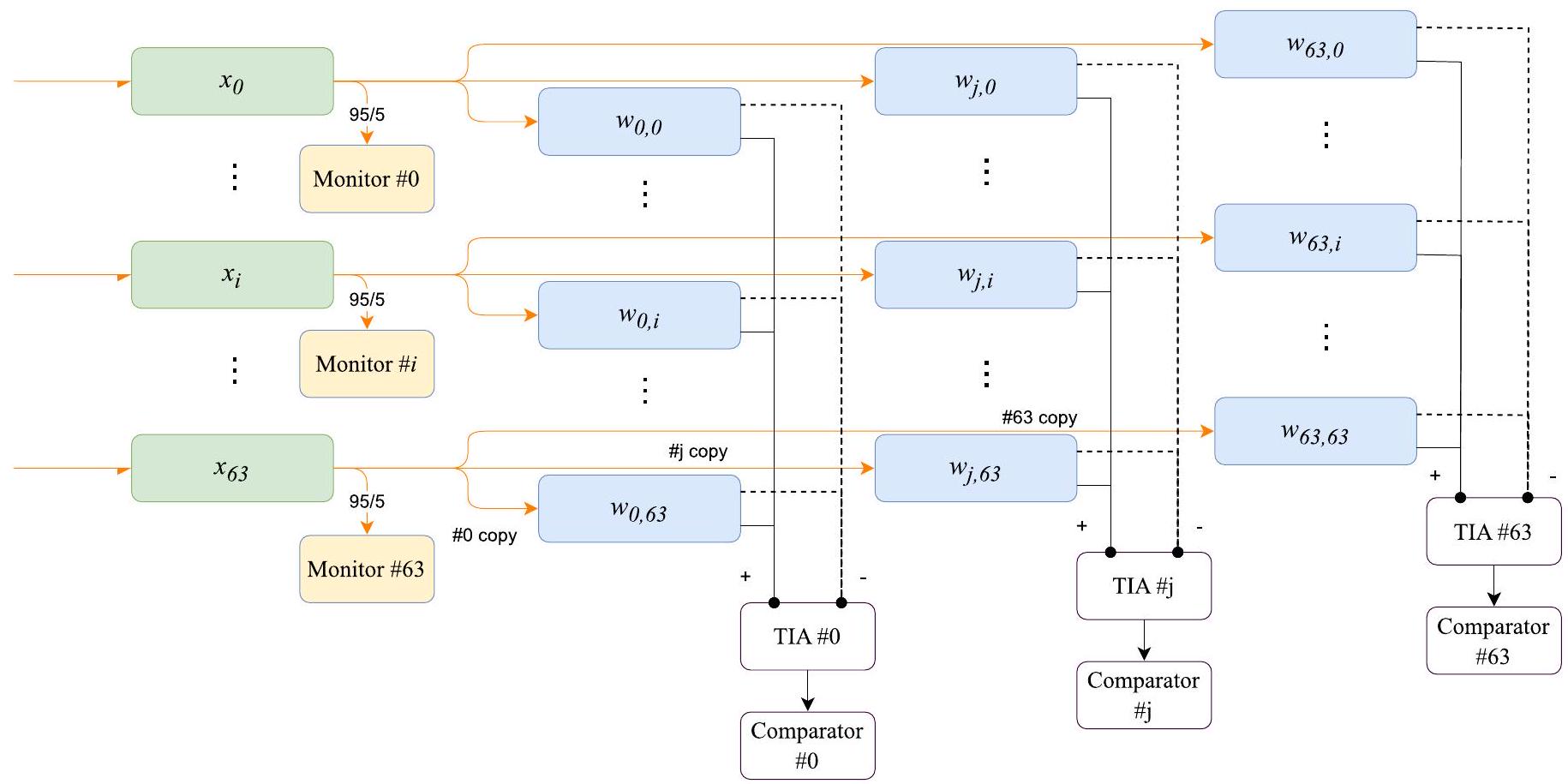
Extended Data Fig. 1 | Architecture of the PACE matrix-vector multiplier. The orange lines represent the optical signals and the dashed and solid black lines represent the electrical signal. The solid or dashed lines before entering the TIA represent a pair of differential signals.
Article
Extended Data Fig. 2 | The electrical-to-optical/optical-to-electrical response of the modulator and photodetector. a, S21 response of the weight modulator used in the PIC.b, S21 response of the photodetectors used
b
in the PIC. The data points represent the mean values of device specs in the system, and the shaded areas denote the min-max ranges.
Extended Data Fig. 3 | Calibration of vector element and matrix element. a, Normalized transmission curve of the DAC digital code sweeping for a vector element channel. b, Purified curve of a matrix element and also the mapping from numerical value ( -4 to 3 ) to DAC codes.
Extended Data Fig. 4 | Matrix-vector multiplication accuracy. a, oMAC results versus true values. The dashed line corresponds to the function ‘ and the orange points are the oMAC calculation results. , Distribution of
single dot-product operation, which shows an average error of -0.06 LSB and a standard deviation of 1.37 LSB.
Extended Data Fig. Energy change during iterations. a, Example of convergence when the laser is on.b, Example of an unconverged case. The dashed line represents the target energy state. When the target energy is achieved within 5,000 iterations, it is considered converged.
a
Extended Data Fig. 6 | The Ising workflows. a, Workflow of the PACE system, in which a dedicated circuit for energy calculation is designed that can run in parallel with the iterations.b, Workflow of the A10 GPU, in which the iterations and energy calculations are performed sequentially.
Extended Data Fig. 7 | Latency comparison of the A10 GPU and PACE schemes. The red line shows the latency of self-defined operators, which is optimized on the basis of the listed action items. The blue line is the latency of using NVIDIA’s cuBLAS library. The black line is the estimated latency using the PACE scheme.
Doerr, C. R. Silicon photonic integration in telecommunications. Front. Phys. 3, 37 (2015).
Li, N. et al. A progress review on solid-state LiDAR and nanophotonics-based LiDAR sensors. Laser Photonics Rev. 16, 2100511 (2022).
Luan, E., Shoman, H., Ratner, D. M., Cheung, K. C. & Chrostowski, L. Silicon photonic biosensors using label-free detection. Sensors 18, 3519 (2018).
Shastri, B. J. et al. Photonics for artificial intelligence and neuromorphic computing. Nat. Photonics 15, 102-114 (2021).
LeCun, Y., Bengio, Y. & Hinton, G. Deep learning. Nature 521, 436-444 (2015).
He, K., Zhang, X., Ren, S. & Sun, J. in Proc. 2016 IEEE Conference on Computer Vision and Pattern Recognition (CVPR) 770-778 (IEEE, 2016).
Krizhevsky, A., Sutskever, I. & Hinton, G. ImageNet classification with deep convolutional neural networks. Advances in Neural Information Processing Systems 25 (NIPS 2012) 1-9 (2012).
Shen, Y. et al. Deep learning with coherent nanophotonic circuits. Nat. Photonics 11, 441-446 (2017).
Lin, X. et al. All-optical machine learning using diffractive deep neural networks. Science 361, 1004-1008 (2018).
Feldmann, J., Youngblood, N., Wright, C. D., Bhaskaran, H. & Pernice, W. H. P. All-optical spiking neurosynaptic networks with self-learning capabilities. Nature 569, 208-214 (2019).
. et al. 11 TOPS photonic convolutional accelerator for optical neural networks. Nature 589, 44-51(2021).
Feldmann, J. et al. Parallel convolutional processing using an integrated photonic tensor core. Nature 589, 52-58 (2021).
Chen, Z. et al. Deep learning with coherent VCSEL neural networks. Nat. Photonics 17, 723-730 (2023).
Xu, Z. et al. Large-scale photonic chiplet Taichi empowers 160-TOPS/W artificial general intelligence. Science 384, 202-209 (2024).
Chen, Y. et al. All-analog photoelectronic chip for high-speed vision tasks. Nature 623, 48-57 (2023).