تاريخ الاستلام: 30 يوليو 2024 تم القبول: 20 فبراير 2025 معاينة المقال المعجلة استشهد بهذا المقال كالتالي: فريق PsiQuantum. منصة قابلة للتصنيع للحوسبة الكمومية الضوئية. ناتشرhttps://doi.org/10.1038/s41586-025-08820-7 (2025)
فريق PsiQuantum
هذا ملف PDF لورقة بحثية تمت مراجعتها من قبل الأقران وتم قبولها للنشر. على الرغم من أنها غير محررة، فقد خضعت المحتويات لتنسيق أولي. تقدم Nature هذه النسخة المبكرة من الورقة المطبوعة كخدمة لمؤلفينا وقرائنا. ستخضع النصوص والرسوم البيانية لعملية تحرير وتدقيق قبل نشر الورقة بصيغتها النهائية. يرجى ملاحظة أنه خلال عملية الإنتاج قد يتم اكتشاف أخطاء قد تؤثر على المحتوى، وتطبق جميع الإقرارات القانونية.
منصة قابلة للتصنيع للحوسبة الكمومية الضوئية
فريق PsiQuantum
الملخص
بينما تحمل وعودًا كبيرة من حيث انخفاض الضوضاء وسهولة التشغيل والشبكات [1]، تم استبعاد الحوسبة الكمومية الضوئية المفيدة بسبب الحاجة إلى مكونات تتجاوز أحدث التقنيات، والتي يتم تصنيعها بالملايين [2-6]. هنا نقدم منصة قابلة للتصنيع [7] للحوسبة الكمومية باستخدام الفوتونات. نقوم بتقييم مجموعة من الوحدات المتكاملة أحاديًا القائمة على الفوتونيات السيليكونية لتوليد ومعالجة وشبك وكشف الكيوبتات الضوئية المعلنة، مما يظهر كيوبتات ضوئية ذات مسارين معتحضير الحالة وموثوقية القياس، تداخل هونغ-أو-ماندل الكمي بين مصادر الفوتونات المستقلة معالرؤية، دمج الكيوبتات الثنائية معالولاء، وواجهة ربط كيوبيت من شريحة إلى شريحة معالوفاء، مشروطًا بالكشف عن الفوتونات ودون احتساب الفقد. نقدم لمحة عن مجموعة من تقنيات الجيل التالي – موجّهات السيليكون النيتريد ذات الفقد المنخفض والمكونات لمعالجة الفقد، بالإضافة إلى مصادر الفوتونات المقاومة للتصنيع، وكواشف الفوتونات عالية الكفاءة القادرة على تحديد عدد الفوتونات، وموصلات الشريحة إلى الألياف ذات الفقد المنخفض، ومحولات الطور الكهروضوئية من الباريوم التيتانات لأداء عالي وسرعة تبديل سريعة.
المقدمة
لقد تم فهم منذ فترة طويلة أن الحواسيب الكمومية المفيدة ستحتاج إلى تصحيح الأخطاء من أجل التشغيل المقاوم للأخطاء، وبالتالي ستحتاج إلى ما يقرب من ملايين الكيوبتات الفيزيائية. بسبب خصائصها المنخفضة الضوضاء بطبيعتها، تم استخدام الفوتونات لتنفيذ العديد من العروض التأسيسية للتراكب، والتشابك، وبوابات المنطق، والخوارزميات، إلخ. ومع ذلك، تم استبعاد الحوسبة الكمومية الضوئية على نطاق واسع حتى الآن بسبب عدد من المتطلبات المعلقة والتحديات.
منذ أولى الاقتراحات لآلات الحوسبة الكمومية الضوئية المقاومة للأخطاء [2-6]، كان من الواضح أنه سيكون هناك حاجة إلى عدد كبير جدًا من المكونات الضوئية لأي نظام مفيد [9، 10]. علاوة على ذلك، لتلبية متطلبات رموز تصحيح الأخطاء، يجب أن تؤدي هذه المكونات أيضًا بشكل يتجاوز أحدث ما توصلت إليه تقنيات الفوتونيات المتكاملة التقليدية [9، 10]، ويجب أن تمتد أيضًا خارج نطاق مكتبة الفوتونيات النموذجية، مما يقدم أجهزة غير قياسية – وأبرزها كاشفات الفوتونات الفردية عالية الكفاءة [11، 12]. إن الحاجة إلى عدد كبير جدًا من الأجهزة المتطابقة تقريبًا تحفز التركيز على التصنيع باستخدام عمليات تصنيع أشباه الموصلات التقليدية عالية الحجم [7]. أخيرًا، يجب دمج هذه الأجهزة معًا في نظام واسع – مما يتطلب إلكترونيات تحكم سريعة، وتبريد كريوجيني عالي الطاقة لدعم تشغيل الكاشفات الفائقة التوصيل، وشبكات منخفضة الفقد وعالية الدقة من الكيوبتات بين الوحدات.
في هذه الورقة، نصف مجموعة تكنولوجيا وكتل بناء أساسية للحوسبة الكمومية الضوئية، موضحين الوظائف الحيوية لتوليد الكيوبتات، ومعالجتها، واكتشافها، والشبكات، بما في ذلك مصادر الفوتونات الفردية، وكواشف الفوتونات الفردية فائقة التوصيل المدمجة في الموجات، وتحضير وقياس حالة الكيوبت الفردي (SPAM)، والاتصالات بين الشرائح للكيوبتات، والتداخل الكمومي للفوتونين، ودمج الكيوبتين؛ كل ذلك عند أطوال موجية للاتصالات (نطاق C). تشكل هذه العمليات الأساسية المطلوبة لمعظم الأساليب في الحوسبة الكمومية الضوئية [2-6، 9]، بما في ذلك الحوسبة الكمومية المعتمدة على الاندماج (FBQC، التي تم تقديمها مؤخرًا في [13]). يتم تصنيع هذه المكونات في مصنع أشباه الموصلات التجاري [14]، باستخدام تقنية متكاملة بالكامل- عملية تدفق الفوتونيات السيليكونية المتكاملة بقطر 300 مم، مع جميع العمليات على الشريحة.
لدخول نظام التشغيل المقاوم للأخطاء، سيتطلب ذلك مجموعة تكنولوجية مع تحسين أداء المكونات ووظائف إضافية. ولهذا الغرض، قمنا بتطوير وتقديم مكونات الجيل التالي، مع خسائر في موجة السيليكون تصل إلى أدنى مستوى منالفواصل والمعابر مع و خسائر الربط بين الألياف والرقائق منخفضة تصل إلىنتائج قياس الكوانتم المقدمة هنا مشروطة بالكشف عن الفوتونات، وإنتاج الفوتونات مُعلن ولكنه غير حتمي. للتغلب على عدم الحتمية في الحوسبة الكوانتية الضوئية، هناك حاجة إلى مفتاح ضوئي سريع للتعددية [15-18]. هنا نقدم مفاتيح تيتانات الباريوم في تقنيتنا لهذا الغرض، مع منتج فقدان الجهد. بالإضافة إلى ذلك، نعرض مصادر فوتونية قوية قادرة على توليد فوتونات غير قابلة للتمييز على مدى تحول الرنين، وكاشفات دقة عدد الفوتونات المدمجة في الموجات الضوئية معكفاءة متوسطة لفوتون واحد، ودقة تصل إلى 4 فوتونات. عند جمعها معًا، تشكل هذه المكونات الجديدة والمحسّنة مجموعة كاملة من الكتل البنائية الضوئية التي تحتوي على جميع الوظائف اللازمة لتمكين أنظمة الحوسبة الكمومية الضوئية المقاومة للأخطاء في المستقبل.
II. مجموعة التكنولوجيا وكتل البناء
تعتبر الفوتونيات السيليكونية تقنية تصنيع ناضجة، مبنية على عقود من التطوير الصناعي لتطبيقات راسخة في قطاعات الاتصالات والطب والسيارات. لقد قمنا بتعديل تدفق تصنيع الفوتونيات السيليكونية القائم ليشمل الكشف عن الفوتونات الفردية عالية الأداء وتوليد أزواج الفوتونات. حسب علمنا، هذه هي المرة الأولى التي يتم فيها تحقيق منصة تقنية فوتونية متكاملة قادرة على توليد ومعالجة وكشف الكيوبتات الفوتونية على الشريحة.
تم تطوير مجموعة تقنياتنا الأساسية في مجال الفوتونيات الكمية بالتعاون مع GlobalFoundries، ويتم تصنيعها في مصنعهم المتقدم لتصنيع أشباه الموصلات بحجم 300 مم. من خلال الاستفادة من خطوات العمليات الصناعية في تصنيع أشباه الموصلات بالاقتران مع خدمات تصميم المصانع، مثل تصحيح القرب البصري وقواعد تصميم العمليات المحسّنة، تكتسب التكنولوجيا قابلية التوسع والأداء من بيئة تجارية عالية الحجم. تشمل عملية التصنيع أكثر من 20 مستوى فوتوغرافي ومئات من خطوات المعالجة والقياس في الخط. تشمل الوحدات الحرجة التي تم تطويرها موجّهات ضوئية سلبية مصنوعة من السيليكون على العازل (SOI)، وطبقة فائقة التوصيل من نيتريد النيوبيوم (NbN) للكشف عن الفوتونات الفردية، وخنادق مليئة بالمعادن العميقة لتقليل الضوضاء الضوئية، وسخانات مقاومة للتحكم في الطور وإعادة تكوين الدوائر الضوئية، ومقابس شبكية للإدخال/الإخراج الضوئي (I/O)، وموصلات كهربائية نحاسية في نهاية الخط، وطبقات إعادة توزيع الألمنيوم.
باستخدام هذه المجموعة، نبني دوائر متكاملة ضوئية كمومية باستخدام مكونات موجات ضوئية سيليكونية قياسية، بما في ذلك الموصلات الاتجاهية، والتقاطعات، ومغيرات الطور الحرارية. نجمع هذه المكونات لإنتاج اللبنات الأساسية: مصادر أزواج الفوتونات العفوية عالية الدقة؛ أجهزة التداخل لإعادة تكوين الدائرة، ومعالجة الكيوبت، والترشيح؛ وكاشفات الفوتون الفردي المدمجة في الموجات الضوئية (الشكل 2أ). الآن نوضح أداء كل من هذه اللبنات الأساسية.
مصادر الفوتونات. من أجل بناء حالات موارد متشابكة، وبالتالي شفرة تصحيح الأخطاء، تستهلك الحواسيب الكمومية الضوئية العديد من الفوتونات الفردية، التي يجب أن تُنتج بكفاءة عالية، وتوقيت محدد جيدًا، ومعدل تكرار مرتفع، بينما تكون أيضًا نقية طيفيًا وغير قابلة للتمييز. تستخدم مصادر الفوتونات الفردية لدينا خلط الموجات الأربعة العفوي (SFWM) المدفوع بواسطة مضخة ليزر نبضي، حيث تكون عملية توليد فوتون فردي احتمالية ولكن يتم الإشارة إليها من خلال اكتشاف زوجها – مما يجعلها مصدر فوتون فردي مُشير (HSPS).
تكون رؤية تداخل الكم الثنائي الفوتون، وهو عملية رئيسية في الحوسبة الكمومية الضوئية، محدودة بنقاء الطيف للفوتونات الفردية المعلنة، والذي يتحدد بكثافة الطيف المشترك لأزواج الفوتونات. نحن نستخدم هياكل موجات ضوئية قائمة على الرنانات لتشكيل الخصائص الطيفية لمصادر الفوتونات لتحقيق نقاء طيفي عالٍ. يتم محاذاة المضخة مع تردد الرنين وتُنتج الفوتونات الفردية عند ترددات رنينية متباعدة بشكل متناظر حولها، كما هو موضح بالأشرطة المظللة في الشكل 2c. تكون مصادر الرنانات ذات الحلقة الواحدة محدودة بطبيعتها بنقاء فوتون معلن قدره [23]. نتجاوز قيود النقاء الطيفي لمصادر الرنانات الفردية باستخدام تصاميم رنانات مرتبطة بالتداخل [23]، والتي قمنا بتوصيفها لتكون لها نقاء طيفي مقاس قدره بدون تصفية طيفية (الشكل 2ب) [24].
كشف الفوتونات. يعتمد الحوسبة الكمومية الضوئية على الإشارة إلى إنشاء حالات كمومية من خلال كشف الفوتونات المتزامنة. تشمل الأمثلة الإشارة إلى فوتون مفرد من مصادر الأزواج، وتوليد حالات موارد احتمالية معلنة، وقياسات الاندماج. من أجل تحمل الأخطاء، تتطلب هذه الوظائف كشف فوتونات مفردة بكفاءة قريبة من الوحدة. قمنا بإدخال طبقة من نيتريد النيوبيوم (NbN) في هيكلنا الضوئي لتمكين كاشفات فوتونات مفردة فائقة التوصيل (SNSPDs) القابلة للتصنيع عالية الأداء.
نستخدم تصميم SNSPD على شكل دبوس شعر [25]، كما هو موضح في الشكل 2a، بسمك فيلمعرض السلك النانوي لـ وطول الكاشف. عند التشغيل في درجة الحرارة، تظهر هذه الكواشف هضابًا واضحة في معدل عدد الفوتونات مقابل تيار الانحياز (الشكل 2e وخرائط الرقاقة في [24])، مما يشير إلى كفاءة كشف داخلية عالية. يتم قياس كفاءة الكشف على الرقاقة من خلال قياسات كهربائية بصرية عند درجات حرارة منخفضة لكواشف SNSPD المدمجة في الموجات الضوئية [24]. أسفرت اختبارات كواشف SNSPD المصفاة عن كفاءة متوسطة على الرقاقة تبلغوقيمة متوسطة لـ [24]، مقيد بتصميم دبوس الشعر للكاشف.
المحولات الضوئية والفلاتر. تُعتبر المحولات الضوئية عنصرًا أساسيًا في الحوسبة الكمومية الضوئية المتكاملة، حيث تمكّن من إعداد حالة الكيوبت وإسقاطها، وتصفية المضخات، وشبكات التبديل، وتوليد حالات الموارد، وقياسات الاندماج. نستخدم تركيبات من الموصلات الاتجاهية، والتقاطعات، والحلقات لبناء الرنانات الحلقية والمحولات الضوئية من نوع ماخ-زنيدر. تم تحسين هذه المكونات من خلال دورات تصميم-اختبار وتوفر أداءً يمكن التنبؤ به مضمونًا من خلال التحكم الصارم في عملية التصنيع. مثال على تداخل ماخ-زنيدر عالي التباين، تم قياسه باستخدام HSPS وSNSPDs المتكاملة، موضح في الشكل 2d، معنسبة الانقراض.
تكون هذه الدوائر السلبية قابلة لإعادة التكوين عند الترددات المنخفضة باستخدام محولات الطور الحرارية، التي تعتبر شائعة في الفوتونيات السيليكونية. بينما يتم تبريد الدائرة نفسها إلى درجة حرارة منخفضة للغاية (لدعم تشغيل كاشفات الفوتونات الفردية الفائقة التكامل)، تصل المحولات الحرارية إلى درجات حرارة محلية تتجاوز بكثيرأثناء التشغيل. بالنظر إلى القدرة المتاحة للتبريد لكل وحدة مساحة عندتعتبر درجات الحرارة الكريوجينية، والعزل الحراري لمغير الطور – باستخدام مناطق محفورة من الركيزة السيليكونية (الشكل 1أ، ب، ي) – أمرًا حاسمًا لتحقيق كفاءة كافية. معظم، إن لم يكن جميع، هذه السخانات أصبحت زائدة عن الحاجة وسيتم إزالتها في النهاية بفضل تقنيات الجيل الثاني الموصوفة لاحقًا في هذه المخطوطة – لا سيما المصدر المقاوم للتصنيع، الذي لن يتطلب ضبطًا، بالإضافة إلى مغير الطور الكهروضوئي، الذي يمكن أن يعمل بمعدلات جيجاهرتز.
III. دوائر توليد الفوتونات الفردية المدمجة والمميزة وقياس الأداء الكمي
حتى الآن، كانت منصات الحوسبة الكمومية الضوئية تعتمد على مصادر الفوتونات الفردية خارج الرقاقة، وكاشفات الفوتونات الفردية خارج الرقاقة، أو كليهما. بينما يكفي ذلك لأغراض العرض، فإنه من الصعب جداً تحقيق كفاءة الإشعار وكثافة المكونات المطلوبة للحوسبة الكمومية المقاومة للأخطاء دون التكامل المشترك للمصدر، والمرشح، وكاشف الإشعار. من خلال دمج عناصرنا الأساسية في منصتنا شبه الموصلة، قمنا بتطوير أول مصدر فوتون فردي معتمد بالكامل ومتكامل في العالم – بما في ذلك المصدر، والترشيح، والإشعار على نفس الرقاقة. باستخدام هذا، نقوم ببناء دوائر كمومية مرجعية لقياس أداء الربط بين الكيوبتات الفردية، والكيوبتات الثنائية، والربط بين الرقائق، والذي يتم تلخيصه في الجدول I.
قمنا باختيار رقائق ضوئية من ألواح 300 مم باستخدام اختبارات كهربائية وبصرية وإلكترونية بكمية كبيرة في الخط وفي نهاية الخط عند درجة حرارة الغرفة؛ بالإضافة إلى الاختبارات عند درجات حرارة منخفضة. اختبار الكهروضوئية لأجزاء مختارة. بالنسبة لأنظمتنا الأكثر تعقيدًا، نقوم بتجميع هذه الشرائح في مجموعات (الشكل 1d) مع مبردات حرارية، وأكثر من 1000 اتصال كهربائي وما يصل إلى 200 إدخال/إخراج بصري. نقوم بتخزين هذه الحزم في أجهزة التبريد.درجة الحرارة الأساسية وقدرة تبريد تصل إلى 20 واط (الشكل 1k).
مصدر الفوتون الفردي المعلن عنه. يتطلب مصدر HSPS عالي الأداء مصادر SFWM مصممة، وكواشف إعلان، بالإضافة إلى شبكة فلاتر عالية الأداء على الشريحة، والتي سنقوم بوصفها الآن. لفصل مضخة الليزر الساطعة عن الفوتونات الفردية، نحتاج إلى suppression of the pump photons. لتحقيق ذلك في دائرة متكاملة، نقوم بدمج كل من التصفية التداخلية داخل الدليل، ودرع الكاشفات من الضوء المضخّم المتناثر خارج الدليل. تستخدم التصفية داخل الدليل سلسلة من المحولات التداخلية غير المتناظرة من الدرجة الأولى والثالثة، مجتمعة مع الرنانات المضافة والمزيلة، لاختيار رنينات مصدر فردية للفوتونات الهرالدية وفوتونات الإشارة. من خلال تحسين النطاق الطيفي الحر وقيم الاقتران لكل عنصر، نحقق رفض المضخة من (الشكل 2ج) [24]، والرفض المتزامن للعمليات البارامترية غير المرغوب فيها. يتم نقل الإشارة وفوتونات الهيرالد عبر شبكات الفلاتر مع فقدان يبلغ حوالي 1 ديسيبل. لقمع الضوء المتناثر، نقوم بحماية الكاشفات محليًا عن طريق إحاطتها بالمعادن (الشكل 1أ، ب، ج). تم بناء الدروع من خنادق معدنية عميقة وضحلة، والمعادن في نهاية الخط. نلاحظ تقريبًا 115 ديسيبل من قمع طاقة المضخة بين مدخل المضخة وSNSPDs.
سمحت الفلاتر المدمجة ودرع الضوء المتناثر، جنبًا إلى جنب مع التكامل المشترك لـ SFWMs وSNSPDs، بأول عرض، حسب علمنا، لإنتاج فوتونات مفردة مدمجة ومبشرة ناجحة على الشريحة، بمعدلات تزامن إلى حادثات (CAR [27]) تصل إلى 3000 [24].
تحضير وقياس حالة الكيوبت المفرد (SPAM). نقوم بتحضير كيوبت مشفر بالطريق [28،29] باستخدام فوتون مُعلن ومُتداخلات ثنائية الوضع، كما هو موضح في الشكل 3a. نقوم بقياس الكيوبت المشفر بالطريق باستخدام مُتداخل ثنائي الوضع وكاشفات فوتونات فائقة السرعة (SNSPDs). يتم التحكم في حالة الفوتون المفرد في وضعي الضوء بواسطة محولات طور حراري، مما يتيح تشفير حالات كيوبت عشوائية. نلاحظ متوسط دقة تحضير وقياس الكيوبت المفرد (الشكل 3e)، مشروطًا باكتشاف الفوتون [24]. بهدف فصل تأثير نسبة إشارة الضوضاء (SNR) لنظام HSPS، نكرر القياس على شريحة مختلفة ولكن مكافئة، باستخدام ضوء متماسك ساطع وكاشفات ضوئية خارج الشريحة، محققين درجة موثوقية [24]، مما يظهر أن دقة SPAM الأعلى ستكون ممكنة مع تحسين نسبة الإشارة إلى الضوضاء في HSPS.
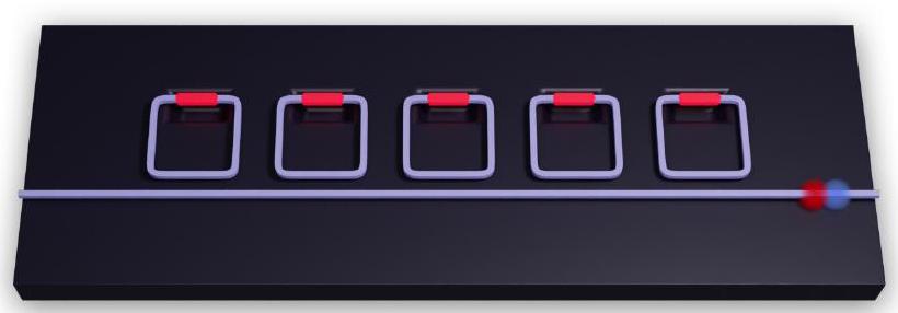
الاتصال بين الكيوبتات من شريحة إلى شريحة. لقد شهدت شبكة الوحدات الكمومية اهتمامًا متزايدًا حيث تسعى تقنيات مختلفة للتوسع خارج حدود شريحة واحدة أو فخ أو شبكة. الكيوبتات الضوئية بطول موجة الاتصالات مناسبة بشكل طبيعي للنقل عبر الألياف الضوئية، دون الحاجة إلى تحويل كمومي. بالإضافة إلى ذلك، يمكن أن يمكّن الاتصال القائم على الألياف الضوئية من وظائف جديدة إضافية مثل التداخل وتجميع الحجم النشط، مما يؤدي إلى توفير كبير في الموارد لخوارزميات مقاومة الأخطاء. لإظهار قدرة الشبكات في الكيوبتات الضوئية التي نبنيها، نقوم بإنشاء شبكة كيوبيت نقطة إلى نقطة (الشكل 3ب) ونقيم دقة الكيوبتات بعد انتقالها بين الوحدات. نقوم بتحضير حالات كيوبيت فردية عالية الدقة باستخدام نفس دائرة تحضير حالة الكيوبت كما هو موضح أعلاه، ونحولها إلى ترميز الاستقطاب باستخدام محول مسار إلى استقطاب قائم على موصل شبكي ثنائي الأبعاد [33]. نقوم بنقل الكيوبت عبر 42 مترًا من الألياف البصرية القياسية المستخدمة في الاتصالات، قبل تحويله إلى ترميز المسار في الوحدة المستقبلة وإجراء قياس حالة الكيوبت على الرقاقة. تستخدم كل من وحدات الإرسال والاستقبال كاشفات فائقة التوصيل على الرقاقة، وتعمل عند درجة حرارة الهيليوم السائل. لقد حددنا مصفوفة نقل باولي [26] لدقة القناة الفيزيائية وعمليات الهوية، مشروطة بوصول الفوتون، لتكون (الشكل 3g) [24]. يظهر النظام خسارة عالية مرتبطة بترابط الألياف مع الرقاقة بواسطة موصلات الشبكة ( الخسارة)، التي سيتم التغلب عليها في الأنظمة المستقبلية باستخدام الأجهزة المتصلة بالحافة (المناقشة أدناه).
تداخل الكم الضوئي ثنائي الفوتون. لتقييم مصادر الفوتون الفردي المتكاملة لدينا، نقوم بقياس تداخل هونغ-أو-ماندل (HOM) الكمومي بين الفوتونات المعلنة من مصدرين مستقلين مدمجين على نفس الشريحة (الشكل 3c). تعتمد الرؤية المقاسة على العديد من العوامل بما في ذلك عدم التمييز، نقاء الطيف، نقاء العدد، نسبة الإشارة إلى الضوضاء، وكفاءة الكشف في النظام. للتحكم في هذه العوامل، نقوم بتنفيذ نظام واحد يدمج التقنيات الموضحة أعلاه: مصادر أزواج الفوتونات عالية النقاء، شبكة مرشحات عالية الانقراض، وكاشفات SNSPD عالية الكفاءة ومحمية.
التداخل الكمي HOM على الرقاقة بين الفوتونات المعلنة من مصادر مختلفة، دون تصفية طيفية كبيرة، كان (الشكل 3f)، والذي نعلم أنه الأعلى المسجل في أي منصة. تم إجراء التجربة بمعدل تكرار مضخة يبلغ 125 ميجاهرتز، مع مصدر CAR منمبشر0.00024، وأقصى كفاءة كليشكو لـ [24].
دمج الكيوبتات الثنائية. دمج بيل هو قياس مشروطي على حالات بيل الثنائية وهو المثال النموذجي لفئة القياسات التي تدعم نموذج FBQC [13]. نقوم بتنفيذ دمج بيل باستخدام قياسات دمج من النوع الثاني [6] على كيوبتات ذات سكة مزدوجة. يستخدم دمج النوع الثاني دائرة بصرية خطية بأربعة أوضاع تليها كشف الفوتونات. يتطلب كل من تداخل الكيوبت الفردي والتداخل بين الكيوبتات، مما يتطلب تحضيرات كيوبت عالية الأداء وتداخل كمي ثنائي الفوتون عالي الوضوح، على التوالي.
نظهر أن عملية الاندماج يمكن أن تؤدي إلى إسقاط عالي الدقة على حالة بيل، باستخدام دائرة القياس في (الشكل 3d). يتم تحضير كيوبتين مفردين مشفرين بشكل مستقل في حالة المنتج.. باستخدام شبكة قياس اندماج قابلة لإعادة التكوين، يتم تبادل المسارات بين الكيوبتات ويتم قياس الحالة الناتجة من خلال قياسات الكيوبت الفردي. عندما يتم الكشف عن فوتون في كل زوج من الكاشفات، نقيس درجة الوفاء بـمع حالة بيل المثالية. يتم عرض مصفوفة الكثافة في الشكل 3h.
الرابع. تقنيات الجيل القادم
أداء تقنية الأساس الموصوفة أعلاه لا يزال غير كافٍ للحوسبة الكمومية الضوئية المفيدة. على وجه الخصوص، تعاني الموجّهات السيليكونية من خسائر انتشار كبيرة جدًا تجعلها غير مناسبة للتسامح مع الأخطاء، وتتطلب مصادر الفوتونات ضبطًا معقدًا واستهلاكًا كبيرًا للطاقة، كما أن التبديل البصري عالي السرعة ضروري بشكل لا مفر منه للتغلب على عدم الحتمية الجوهرية لمصادر الفوتونات الفردية العفوية.
نحن الآن نصف بعض التطورات الحاسمة نحو أداء أعلى ووظائف إضافية في منصات التكنولوجيا من الجيل التالي لدينا، المستمدة من تدفقات عمليات متعددة. نركز على مصادر الفوتونات المتقدمة، والكشف عن عدد الفوتونات عالي الكفاءة، والموجّهات ذات الفقدان المنخفض، ودمج الألياف مع الرقائق بكفاءة عالية، ومغيرات الطور الكهروضوئية على الرقاقة.
مصدر الرنان المتسلسل. تعتبر مؤشرات الأداء الرئيسية لمصادر الفوتونات هي وضوح تداخل الفوتونين وكفاءة الفوتون. ومع ذلك، هناك خصائص إضافية يجب معالجتها لتمكين تشغيل الأجهزة على نطاق الحواسيب الكمومية المفيدة. يعتبر متطلبان مهمان هما قوة الضخ المطلوبة لدفع عملية SFWM، والحرارة المفقودة عند درجات حرارة منخفضة للتحكم في المصدر وضبطه. لقد قمنا بتنفيذ مصدر رنان متسلسل يعالج هذه الجوانب في وقت واحد.
يتكون المصدر من عدة رنانات متكاملة مرتبطة بدليل موجي واحد (الشكل 4أ). من خلال التحسين المشترك لاقتران الرنانات مع الدليل الموجي، وأطوال الموجات الرنانة، وسعة الطيف الضوئي للمضخة، يمكن هندسة الكثافة الطيفية المشتركة للمصدر. لقد حقق جهازنا المكون من 24 رنانًا نقاءً محددًا أعلى. [24]، مع افتراض مرحلة طيفية مسطحة (الشكل 4ب)، بينما يتم استخدام طاقة ضخ أقل بمقدار ترتيب من المصدر المتصل بالتداخل. حتى مع الطاقة الأقلمن SiN، يحقق مصدر الرنان المتسلسل المحسن لدينااحتمالية الزوج مع حوالي 100 بيكوجول من طاقة نبضة المضخة، والتي تقع ضمن نطاق مكبرات الإربيوم القابلة للتوسع عند معدلات تكرار جيجاهرتز.
هذا المصدر من الرنانات المتسلسلة يعالج عدم التمييز بطريقة جديدة. طيف أزواج الفوتونات ثابت بواسطة طول موجة المضخة وليس بواسطة الطول الموجي الرنيني للجهاز. وبالتالي، فإن التحولات الرنينة العالمية (مثل تلك الناتجة عن اختلافات التصنيع) لها تأثير ضئيل على عدم التمييز الطيفي للفوتونات الناتجة من أجهزة مختلفة. الشكل 4c، يظهر عدم التمييز المقاس بين مصدرين كدالة لتحول الرنين [24]. باستخدام منظمات حرارية، قمنا بمحاذاة جهازين إلى نقطة التشغيل المثلى وطبقنا تحول رنيني عالمي محكوم على مصدر رنان متسلسل واحد، لمحاكاة تأثير اختلافات التصنيع. في هذا التنفيذ، نحققعدم التمييز بين مصدرين علىنافذة تحول الرنين، مقارنة بأقل منلمصدر ذو حلقة واحدة. يمكن أن تتيح القدرة المدمجة لمصدر الرنان المتسلسل على التفاوت العالمي في الطول الموجي من جهاز إلى آخر، جنبًا إلى جنب مع التحكم المتقدم في التصنيع، مصادر فوتون غير قابلة للتمييز بدون موالف.
كواشف حل عدد الفوتونات (PNRDs). تفتقر كاشفات الفوتونات الفردية المدمجة في الموجات الموجهة القابلة للتصنيع التي تم تقديمها سابقًا، على الرغم من كونها تحويلية، إلى القدرة على تمييز عدد الفوتونات المطلوبة لـ FBQC. إن القدرة على تمييز أعداد الفوتونات المنخفضة في الكشف، والإعلان عن تلك المعلومات، يسمحان بإزالة حالات عدد الفوتونات الأعلى التي يتم توليدها في مصادر SFWM، وتحديد الأحداث غير المرغوب فيها في توليد الحالة المتشابكة المعتمدة على الاندماج والحساب [21].
يمكن استخدام التعدد المكاني [34] للعديد من عناصر الكاشف الشبيهة بـ SNSPD، كما هو موضح في الشكل 4d، لتجميع كاشف قابل للتوسع مع دقة فعالة في عدد الفوتونات. في هذه الكواشف PNRDs، يكون عدد الفوتونات المكتشفة تقريبًا متناسبًا مع سعة جهد خرج الكاشف. للتحقق من هذا المفهوم، قمنا بإنتاج كواشف PNRDs مدمجة في الموجات الضوئية تحتوي على 4 و 5 خلايا وحدات، حيث حققت أفضل التصاميم كفاءات اكتشاف على الرقاقة. (الوسيط) و (المتوسط) (الشكل 4e) [24]. تتمتع هذه الكواشف بالقدرة على حل الفوتونات، كما هو موضح في المدرج التكراري في الشكل 4f [24].
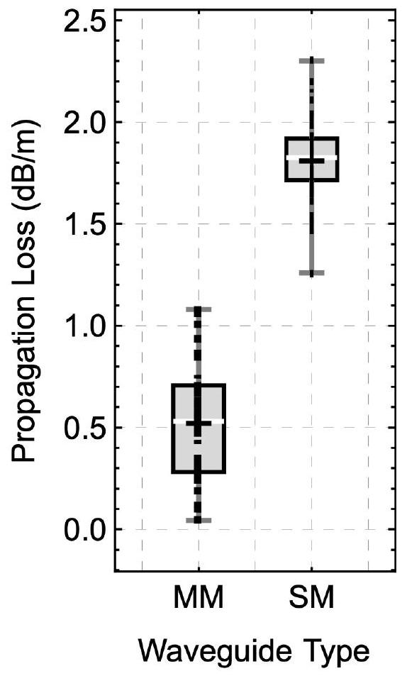
أدلة الموجات من نيتريد السيليكون ذات الخسارة المنخفضة، الموصلات الاتجاهية والتقاطعات. تقتصر أدلة الموجات المصنوعة من السيليكون على العازل في خسارة انتشار الموجات بسبب تباين معامل الانكسار الكبير [35]. من ناحية أخرى، تتمتع أدلة الموجات من نيتريد السيليكون (SiN) بتباين أقل في معامل الانكسار، مما يوفر تسوية جيدة بين الاحتجاز والحساسية لتغيرات التصنيع [35]. لقد أظهرنا خسارة أدلة الموجات من SiN ذات الوضع الواحد منوخسارة الموجة متعددة الأوضاع من (الشكل 5أ)، تم قياسه باستخدام تقنية القطع [24]. في هذه المنصة نفسها، قمنا بتنفيذ تقاطعات موجية معفقدان، ومقسمات الموجات الموجهة معالخسارة (الشكل 5ب) [24]. هذه الخسائر المكونة هيبعيدًا عن قيمة الهدف لدينا بينما خسائر الدليل الموجي في الهدف.
يوفر SiN أيضًا مزايا لتوليد الفوتونات. إن الخسارة المنخفضة للغاية جنبًا إلى جنب مع عدم خطية كير تدعم SFWM مع نسبة إشارة إلى ضوضاء عالية. علاوة على ذلك، هناك غياب للخسارة غير الخطية، مما يسمح للمصادر بالعمل بخسارة منخفضة عند معدلات أزواج عالية، على عكس السيليكون، حيث يؤدي امتصاص الفوتونين إلى تدهور الأداء.
ربط الألياف بالرقائق. يتطلب الربط منخفض الفقد للضوء من الألياف البصرية إلى رقائقنا الكوانتية الفوتونية لجعل الشبكات الألياف عملية. نحن ننفذ تصاميم جديدة لموصل الحواف التي تقلل من تداخل الأوضاع وفقدان تحويل الأوضاع، مما يمكّن من ربط عالي الأداء بين الألياف والرقائق. التحدي الرئيسي هو تحويل وضع الموجة المحصور بشدة في الرقاقة ليتناسب مع الوضع الأكبر بكثير من الألياف البصرية. لقياس فقد الإدخال لموصل الحواف، يتم وضع رقاقة بين الألياف البصرية المدخلة والمخرجة باستخدام مراحل محاذاة بصرية عالية الدقة. تُظهر الشكل 5c قياسات متكررة من اثنين من أفضل تصاميم موصل الرقاقة إلى الألياف لدينا، مع فقدان الربط إلى الألياف البصرية القياسية من فئة الاتصالات (SMF-28) من، وفقدان الاقتران إلى الألياف ذات الفتحة العددية العالية (UHNA4) من.
التبديل الكهروضوئي. من أجل التغلب على عدم الحتمية الجوهرية لكل من المصادر العفوية وبوابات الاندماج، سيتطلب الحوسبة الكمومية الضوئية مفاتيح بصرية عالية السرعة تتجاوز أحدث التقنيات، من أجل تمكين الشبكات البصرية التي يمكن إعادة تكوينها بسرعة بناءً على نتائج توليد الفوتونات المعلنة السابقة، وبوابات التشابك، ونتائج الاندماج. العنصر الرئيسي المطلوب لمثل هذه الشبكات التبديلية هو محول طور كهربائي بصري عالي السرعة ومنخفض الفقد.يمكن بناء الشبكات من خلال تضمين هذا المحول الطوري في أجهزة التداخل السلبية المكونة من مقسمات الشعاع والأجهزة المتقاطعة التي تم وصفها سابقًا [18].
أداء المحول الطوري مقيد أساسًا باختيار المادة الكهروضوئية. نحن ندمج التيتانات الباريوم (BTO) [37] في مجموعتنا الضوئية كمحول طوري كهروضوئي. لقد طورنا عملية حصرية لنمو أفلام BTO عالية الجودة باستخدام تقنية ترسيب الطبقات الجزيئية، المتوافقة مع عمليات المصانع، على رقائق السيليكون كاملة الحجم 300 مم. لقد حققناتجانس السماكةعبر كامل شريحة 300 مم، مع قيم بوكيلز الكهروبصرية لـ (مقارنة بـ لليثيوم نيوبيوم [38])، تم قياسه من خلال قياسات بوكيلز في الفضاء الحر (الشكل 5d).
المزيفتتضمن مفاتيح BTO Mach-Zehnder قسمًا لمغير الطور بطول 2 مم، مع خسارة في الانتشار قدرها (الشكل 5f) و DC من (الشكل 5g) [24]. هذا يعطي خسارة إدخال لمغير الطور قدرها ومنتج جهد فقد نصف الموجة لمغير الطور من، مما يتيح مسارًا لبناء أكبرالشبكات التحويلية ذات الفقد المنخفض المطلوبة للحوسبة الكمومية الضوئية. فقد الإدخال لهذا الجهاز هوبعيدًا عن قيمة هدفنا.
V. الخاتمة
لقد وصفنا التعديلات التي تم إجراؤها على عملية تصنيع أشباه الموصلات الصناعية للضوئيات الكمومية المتكاملة، مما يظهر أداءً قياسيًا. من خلال إضافة مواد وتصاميم وخطوات عملية جديدة، تمكنا من تمكين التصنيع بكميات كبيرة لمصادر الفوتونات المعلنة وكاشفات الفوتونات الفردية فائقة التوصيل، بالإضافة إلى معالجة الفوتونات عبر التداخل، وقابلية الضبط، والتحكم في الضوء غير المرغوب فيه. كما وصفنا أيضًا أجهزة ذات أداء أعلى، نحو حل القيود البارزة لهذه المنصة الأساسية.
الحوسبة الكمومية المعتمدة على الاندماج تدعم بروتوكولات مقاومة للأخطاء يمكنها تحمل مستوى منالخسارة البصرية الإجمالية المتراكمة بين انبعاث الفوتونات والكشف عنها، مع أخطاء لكل كيوبت في شبكة الاندماج من ترتيب 1% [13، 39-41]. هنا، لقد أظهرنا مجموعة كاملة من المكونات البصرية لـ FBQC، كل منها مع خسائر بصرية عند مستوى بضع بالمئة أو أقل، بالإضافة إلى دوائر متكاملة بالكامل تظهر تداخلًا عالي الوضوح، وتوزيعًا ووظائف قياس لكيوبتات الفوتون، جميعها بمستويات خطأ أقل من واحد بالمئة.
لا تزال هناك حاجة لتحسينات على المنصة والعمليات. سيكون من الضروري تقليل خسائر المواد والمكونات SiN بشكل أكبر، وتحسين أداء الفلاتر، وزيادة كفاءة الكاشف لدفع خسارة الفوتونات العامة والموثوقية. بعض الأمثلة المحددة على التحديات المتبقية هي: تنفيذ تقنيات منخفضة الخسارة.تحولات سريعة نحو مصدر فوتون متعدد؛ محاذاة وتغليف قابلة للتكرار لروابط حافة الشريحة إلى الألياف ذات الخسارة المنخفضة للغاية؛ وتحسين استهداف وموثوقية التصاميم الضوئية لتقليل الحاجة إلى الضبط والتقليم باستخدام السخانات، مما يقلل من الحمل الحراري عند درجات الحرارة الكريوجينية.
أخيرًا، نلاحظ أن المنصات التي قمنا بتطويرها، وتحسيناتها المستقبلية، تتمتع بمرونة عالية. ترتيبات المكونات قابلة للتكوين بشكل كبير، مما يجعل النظام مناسبًا لمختلف تنويعات هياكل الحواسيب الكمومية، وتطبيقات تكنولوجيا الكم المختلفة، وكذلك تقنيات ضوئية أخرى. إن القدرة على توصيل الشرائح بواسطة الألياف مع فقدان منخفض جدًا تجعل النظام قابلًا للتوسع تقنيًا عبر أعداد كبيرة من الشرائح الضوئية، وتسمح بإنشاء شبكات مستقبلية أو اتصالات بين أنظمة مختلفة في مجموعة من مجالات التطبيقات. على الرغم من أن الهدف الوحيد من تطويرنا هو حاسوب كمومي مقاوم للأخطاء، نأمل أن يكون تأثير منصتنا الضوئية الكمومية القابلة للتصنيع صناعيًا واسعًا وملموسًا.
الشكر والتقدير: نشكر الدعم المستمر من مستثمرينا وشركائنا والوكالات الحكومية.
مساهمات المؤلفين: تم تصور وتخطيط المنصة وتجارب القياس من قبل فريق PsiQuantum. كانت أقسام هندسة وهندسة النظام في
أنشأت PsiQuantum منهجية تحليل البيانات، والنمذجة، والأدوات المترولوجية التي دعمت التجارب، وجمعت النظام، وتولت عمليات المعايرة، وجمعت البيانات. في الوقت نفسه، كانت الفرق المسؤولة عن المكونات مسؤولة عن تطوير المكونات الضوئية، وأقامت فرق العمليات منصة التصنيع وأجهزة BTO. تم تأليف المخطوطة والمعلومات التكميلية وتحريرها من قبل جميع المؤلفين.
المصالح المتنافسة: يعلن المؤلفون عدم وجود مصالح متنافسة. [1] ج. ل. أوبراين، العلوم 318، 1567 (2007). [2] إ. كنييل، ر. لافلام، و ج. ج. ميلبورن، ناتشر 409، 46 (2001). [3] ت. س. رالف، أ. ج. وايت، و. ج. مونرو، و ج. ج. ميلبورن، فيزيكال ريفيو A 65، 012314 (2001). [4] ن. يوران و ب. ريزنيك، فيزيكال ريفيو ليترز 91، 037903 (2003). [5] م. أ. نيلسن، فيزيكال ريفيو ليترز 93، 040503 (2004). [6] د. إ. براون وت. رودولف، فيزيكال ريفيو ليترز 95، 010501 (2005). [7] هـ. جينغ، دليل تصنيع أشباه الموصلات. الطبعة الثانية (نيويورك: ماكغرو هيل للتعليم، 2018). [8] أ. ج. فاولر، س. ج. ديفيت، و ل. س. ل. هولنبرغ، معلومات الكم. حساب. 4، 237- (2004). [9] ي. لي، ب. س. همفريز، ج. ج. ميندوزا، و س. س. بنجامين، فيز. ريف. إكس 5، 041007 (2015). [10] ت. رودولف، APL فوتونيكس 2، 030901 (2017). [11] ج. ن. غولتسمان، أ. أوكونيف، ج. تشولكوفا، أ. ليباتوف، أ. سيمينوف، ك. سميرنوف، ب. فورونوف، أ. دزاردانوف، ج. ويليامز، و ر. سوبوليفسكي، رسائل الفيزياء التطبيقية 79، 705 (2001). [12] ف. مارسيلي، ف. ب. فيرما، ج. أ. ستيرن، س. هارينغتون، أ. إ. ليتا، ت. جيريتس، إ. فايشينكر، ب. بايك، م. د. شو، ر. ب. ميرين، و س. و. نام، ناتشر فوتونيكس 7، 210 (2013). [13] س. بارتولوكّي، ب. بيرتشال، هـ. بومبين، هـ. كابل، ج. داوسون، م. خيمينيو-سيغوفيا، إ. جونستون، ك. كيلينغ، ن. نيكرسون، م. بانت، ف. باستاوسكي، ت. رودولف، و ج. سبارو، اتصالات الطبيعة 14، 912 (2023). [14] ك. جيونت، ك. نامي، ف. أ. أندرسون، ج. أيا لا، ت. بارويتز، ي. بيان، ك. ك. ديزفوليان، د. م. جيل، ت. هاوتون، س. هو، ب. بينغ، م. راكوفسكي، س. راوخ، ج. س. روزنبرغ، أ. شاهين، إ. ستوبرت، وأ. ستريكر، مجلة IEEE للمواضيع المختارة في الإلكترونيات الكمومية 25، 1 (2019). [15] أ. ل. ميجدال، د. برانينغ، وس. كاستيلتو، فيزيكال ريفيو A 66، 053805 (2002). [16] ت. ب. بيتمان، ب. س. جاكوبس، وج. د. فرانسن، فيز. ريف. أ 66، 042303 (2002). [17] إ. ماير-سكوت، س. سيلبرهورن، و أ. ميجدال، مراجعة الأدوات العلمية 91، 041101 (2020). [18] س. بارتولوكّي، ب. بيرتشال، د. بونوه، هـ. كابل، م. خيمينوسيجوفيا، ك. كيلينغ، ن. نيكرسون، ت. رودولف، و ج. سبارو، (2021)، arXiv:2109.13760 [quant-ph]. [19] س. ي. سيو، ب. لي، ف. قاو، هـ. ي. تشنغ، و. تشانغ، ب. قوه، س. و. شيا، أ. سونغ، ب. دونغ، ل. و. لو، ج. لي، إكس. لو، و ج. كيو. لو، مجلة تكنولوجيا الضوء 39، 4374 (2021). [20] س. شيخار، و. بوجارتس، ل. كروستوسكي، ج. إي. باورز، م. هوشبرغ، ر. سورييف، و ب. ج. شاستري، اتصالات الطبيعة 15، 751 (2024). [21] س. بارتولوكسي، ب. م. بيرتشال، م. جيمينيو-سيغوفيا، إ. جونستون، ك. كيلينغ، م. بانت، ت. رودولف، ج. سميث، س. سبارو، و م. د. فيدريغين، (2021)، arXiv:2106.13825 [quant-ph]. [22] ج. و. سيلفرتون، د. بونيو، ج. ل. أوبراين، و م. ج. طومسون، مجلة IEEE للمواضيع المختارة في الإلكترونيات الكمومية 22، 390 (2016). [23] ز. فيرنون، م. مينوتي، س. س. تيزون، ج. أ. ستايدل، م. ل. فانتو، ب. م. توماس، س. ف. بريبل، أ. م. سميث، ب. م. ألسينغ، م. ليسيديني، وج. إ. سايب، رسالة أوبتيك 42، 3638 (2017). [24] مواد إضافية. [25] إكس. هو، سي. دبليو. هولزوارث، دي. ماسكياريلي، إي. أ. داولر، وكي. كي. بيرغرين، معاملات IEEE على الموصلية الفائقة التطبيقية 19، 336 (2009). [26] ج. م. تشاو، ج. م. غامبيتا، أ. د. كوركوليس، س. ت. ميركل، ج. أ. سمولين، س. ريجتي، س. بوليتو، ج. أ. كيف، م. ب. روثويل، ج. ر. روزن، م. ب. كيتشن، و م. ستيفن، فيز. ريف. ليت. 109، 060501 (2012). [27] ج. سي. بيينفانغ، ج. بيينفانغ، ت. جيريتس، ب. كوو، أ. ميجدال، س. بولياكوف، وأو. تي. سلاتري، IR 8486، وزارة التجارة الأمريكية، المعهد الوطني للمعايير والتكنولوجيا (2023). [28] أ. بوليتي، م. ج. كرايان، ج. ج. راريتي، س. يو، و ج. ل. أوبراين، ساينس 320، 646 (2008). [29] ج. وانغ، ف. سيارينو، أ. لاينغ، و م. ج. تومسون، ناتشر فوتونيكس 14، 273 (2020). [30] ن. لاوك، ن. سينكلير، س. بارزنجاه، ج. ب. كوفي، م. سافمان، م. سبيروبولو، و ج. سيمون، العلوم والتكنولوجيا الكمومية 5، 020501 (2020). [31] هـ. بومبين، إ. هـ. كيم، د. ليتينسكي، ن. نيكرسون، م. بانت، ف. باستاوسكي، س. روبرتس، و ت. رودولف، (2021)، arXiv:2103.08612 [quant-ph]. [32] د. ليتينسكي و ن. نيكرسون، (2022)، arXiv:2211.15465 [quant-ph]. [33] د. لويلين، ي. دينغ، إ. إ. فاروق، س. بايساني، د. باكو، ر. سانتاجاتي، ي.-ج. تشيان، ي. لي، ي.-ف. شياو، م. هوبر، م. مالك، ج. ف. سينكلير، إكس. تشو، ك. روتويت، ج. ل. أوبراين، ج. ج. راريتي، ق. غونغ، ل. ك. أوكزنلو، ج. وانغ، و م. ج. طومسون، ناتشر فيزيكس 16، 148 (2020). [34] س. جاهانميرينجاد وأ. فيوري، أوبت. إكسبريس 20، 5017 (2012). [35] و. د. ساخر، ج. س. ميكليسن، ي. هوانغ، ج. س. ماك، ز. يونغ، إكس. لو، ي. لي، ب. دومايس، ج. جيانغ، د. جودويل، وآخرون، وقائع IEEE 106، 2232 (2018). [36] ل. م. روزنفيلد، د. أ. سولواي، ج. ف. سينكلير، ف. أنانت، م. ج. تومسون، ج. ج. راريتي، وج. و. سيلفرتون، أوبت. إكسبريس 28، 37092 (2020). [37] ف. إلتس، ج. إ. فيلارريال-غارسيا، د. كايمي، هـ. سيغوارت، أ. أ. جنتيلي، أ. هارت، ب. ستارك، ج. د. مارشال، م. ج. تومسون، ج. باريتو، ج. فومبيريين، و س. أبيل، مواد الطبيعة 19، 1164 (2020). [38] د. زو، ل. شاو، م. يو، ر. تشينغ، ب. ديسياتوف، ج. ج. شين، ي. هو J. Holzgrafe، S. Ghosh، A. Shams-Ansari، E. Puma، N. Sinclair، C. Reimer، M. Zhang، و M. Lončar، Adv. Opt. Photon. 13، 242 (2021). [39] إتش. بومبين، سي. داوسون، ن. نيكرسون، م. بانت، وج. سوليفان، (2023)، arXiv:2303.16122 [quant-ph]. [40] إتش. بومبين، سي. داوسون، تي. فارلي، واي. ليو، إن. نيكرسون، إم. بانت، إف. باستاوسكي، وإس. روبرتس، (2023)، arXiv:2308.07844 [quant-ph]. [41] PsiQuantum، مخطوطة قيد الإعداد.
مقياس
قيمة التجربة (%)
كيوبت مفرد
أمان الرسائل غير المرغوب فيها
موثوقية الشريحة إلى الشريحة
زوج من الكيوبتات
رؤية التداخل الكمي
وفاء الجرس
الجدول I. مقاييس أداء الكيوبت الواحد والكيوبتين. دون احتساب الفقد. *تم قياس موثوقية SPAM الثانية المذكورة أعلاه باستخدام ضوء ساطع وكواشف خارج الرقاقة، انظر النص الرئيسي.
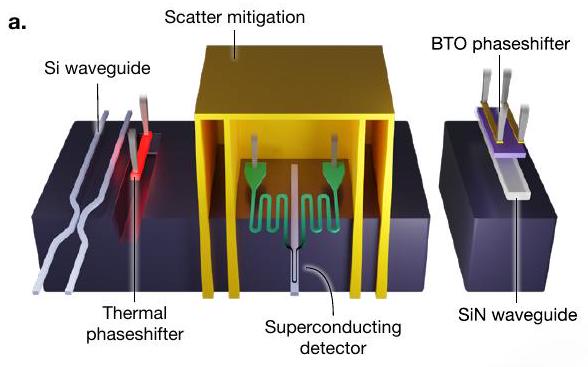
الشكل 1. كومة فوتونية كمومية متكاملة قابلة للتصنيع. و مخطط للمكونات الرئيسية ووحدات العملية. نبرز (على اليمين) خطوات عملية إضافية مدرجة في منصتنا من الجيل التالي. ج، شريحة بقطر 300 مم تحتوي على مصادر فوتونات مفردة، وكاشفات فوتونات مفردة فائقة التوصيل، ودارات تقييم كمي. د، تجميع مبرد يحتوي على شريحة ضوئية، وموزع حرارة، ولوحة دوائر إلكترونية PCB ووحدة توصيل ألياف بصرية للاتصالات مكونة من 100 قناة. هـ-ك، صورة مجهرية بصرية، صور مجهر إلكتروني مس扫描 أو صور مجهر إلكتروني نافذ لـ:مصدر الفوتون (من الأعلى إلى الأسفل)؛دليل الموجات البصرية (المقطع العرضي)؛درع الضوء المتناثر في الخندق العميق/الضحل (مقطع عرضي)؛كاشف الفوتون المفرد (من الأعلى إلى الأسفل)؛خندق العزل الحراري (مقطع عرضي)؛كاشف الفوتون المفرد على الموجّه (مقطع عرضي).جهاز كريوستات مخصص مستخدم في تجارب القياسقدرة التبريد عند 2.2 ك.
الشكل 2. العناصر الأساسية للمنصة. أ، مخططات لمصدر الفوتون، شبكة الفلاتر، المتداخل وكاشف. ب، شدة الطيف المشترك المقاسة لمصدر فوتون متصل بالتداخل، مما يشير إلى نقاء طيفي لـ [24]. ج، استجابة شبكة فلتر المضخة لدينا. نحن نحدد نطاقات تردد المضخة والإشارة والإشارة المعلنة ونظهر طيف الفلتر المقاس للإشارة المعلنة (باللون البرتقالي) والإشارة (باللون الأزرق)، المميز باستخدام SNSPDs على الشريحة. د، الاستجابة المقاسة لمتداخل ماخ-زنر (MZI) للإضاءة أحادية الفوتون المعلنة على منصة متكاملة بالكامل. نسبة الانقراض عند منفذ النقل هي إن عدم التماثل في استجابة MZI هو نتيجة لعدم ثبات حجم الخطوة، الذي يكون أدق حول ميزة واحدة فقط. لا يوجد تباين كبير في الأداء عبر الدائرة أو بين دوائر مختلفة. e، تم قياس كفاءة الكشف على الرقاقة كدالة لتيار انحياز الكاشف ( ) مُعَدل بواسطة تيار تبديل الكاشف ( )، و(في الزاوية السفلية اليمنى) معدل عدّ الكاشف (باللون الأزرق) ومعدل العدّ المظلم (باللون البرتقالي) في الثانية [24].
الشكل 3. دوائر قياس الكم. هذه الدوائر قابلة لإعادة التكوين عبر محولات الطور الحرارية المشار إليها باللون الأحمر في المخططات. مخططات: أ، إعداد وقياس الحالة الكمومية؛ ب، شبكة كيوبيت من نقطة إلى نقطة؛التداخل الكمي ثنائي الفوتون (HOM)؛ د، قياس اندماج الكيوبتات الثنائية. هـ، دقة SPAM للحالة المعاد بناؤها مع الحالة المستهدفة لحالات باولي الذاتية. و، تداخل HOM.مصفوفة نقل باولي المقاسة [26] لقناة الاتصال بين الرقائق الكيوبت.مصفوفة الكثافة المكونة من كيوبتين المعاد بناؤها بعد الاندماج (تشير الأشرطة الرمادية إلى القيم التي تقل عن عتبة 0.01).
الشكل 4. مصدر الرنان المتسلسل وPNRD. أ، مخطط المصدر. ب، شدة الطيف المشترك المقاسة لمصدر الرنانات المتسلسلة التي تظهر حتىالنقاء، مع افتراض الطور الطيفي المسطح [24]. ج، قياس عدم التمييز بين نسختين من المصدر كدالة للازاحة في طول الموجة الرنانة [24]. د، صورة ميكروغرافية بصرية من الأعلى لموصل موجات SiN المرتبط بـ PNRD، حيث تتقاطع كواشف الفوتون الفردي (SNSPDs) مع موصل الموجات وتمتص الضوء من الموصل عبر الاقتران المتلاشي. مجموعات من SNSPDs متصلة عبر مقاومات على الرقاقة لتكوين خلية وحدة. يتم توصيل خلايا الوحدة المتطابقة على التوالي. هـ، كفاءة الكشف على الرقاقة لـ PNRD الموضح في د كدالة للتيار المحايد المنظم، مع عرض المتوسط عبر 6 أجهزة فريدة [24]. هـ-إدراج، توزيع كفاءة الكشف في لقطة واحدة لكل من الأجهزة الفريدة التي تم تحييدها عندعند مستويي طاقة مدخلين. (يسار) مخطط مستمر لإشارة الكشف الضوئي الكهربائي (آثار الجهد) لوحدة PNRD مكونة من 4 خلايا. تم تسجيل الآثار باستخدام مضخم منخفض الحرارة. تظهر آثار الجهد 5 مستويات مميزة، تتوافق مع و 4 خلايا وحدة تكشف الفوتونات في نفس الوقت. (إلى اليمين، رسم بياني لتوزيع الجهد).
الشكل 5. خسارة الموجّه والمكونات، ومفتاح بيوتي. أ، ب، ج، خسارة مكونات قائمة على SiN مع المتوسط (الخط الأسود) والوسيط (الخط الأبيض). أ، قياس خسارة الموجّه SiN، موضحًا النتائج عبر رقائق نموذجية لكل من الموجّهات متعددة الأوضاع (MM) والموجّهات أحادية الوضع (SM) [24]. ب، خسارة مكونات SiN لموزعات الموجّهات والتقاطعات [24]. ج، خسارة من الشريحة إلى الألياف. يتم قياس اقتران الألياف إلى الشريحة في نظام الخسارة المنخفض باستخدام قياسات نقل متكررة على جهازين نموذجيين مصممين لألياف SMF-28 وجهاز نموذجي مصمم لألياف UHNA [24]. د، قياس كهربائي بصري في الفضاء الحر لمعامل بوكيل الفعال لفيلم BTO المزروع بطريقة MBE، مع وجود تذبذب. هـ، مقطع عرضي باستخدام المجهر الإلكتروني الماسح لمحوّل الطور BTO-on-SiN المُصنّع بالكامل. و، قياس خسارة الانتشار المعتمد على القطع لمحوّل الطور BTO-on-SiN (نقاط البيانات وخط الإرشاد)، معفترات الثقة المقدمة (خطوط متقطعة).، قياس النقل البصري لمتداخل ماخ-زيندر (MZI) معمحول طور BTO بطول مم. تم تطبيق جهد على أحد ذراعي MZI، مما أدى إلىف.س مفي تكوين غير دفع-سحب [24]، حيث هو الجهد المطلوب لتغيير الطور بـ راديان. يمكن العثور على خرائط الرقائق لهذه النتائج في المواد التكميلية [24]. د.
ب. مصدر الفوتون
د. مقياس ماخ-زيندر
ج. شبكة الفلترة
e. كاشف فوتونات مفردة من أسلاك نانوية فائقة التوصيل
أ. إعداد وقياس حالة الكيوبت المفرد
ب. الربط بين الكيوبتات
ج. تداخل كمي ثنائي الفوتون
e. وفاء الرسائل غير المرغوب فيها
ز. التداخل الكمي
99.72%
ج. الربط بين الكيوبتات
قياس اندماج الكيوبت
أ. مصدر الرنان المتسلسل
ب. المصدر JSI
ج. عدم التمييز من مصدر إلى آخر
ج. كاشف يحل عدد الفوتونات
كفاءة PNRD على الرقاقة
تقرير PNRD
أ. خسارة موجة SiN
فقدان مكون SiN
قياس فيلم بوكيلز
مقطع عرضي لمغير الطور BTO
شركة PsiQuantum، بالو ألتو 94304 كاليفورنيا، الولايات المتحدة الأمريكية شركة PsiQuantum المحدودة، دارسبرى WA4 4FS، المملكة المتحدة
A manufacturable platform for photonic quantum computing
Received: 30 July 2024
Accepted: 20 February 2025
Accelerated Article Preview
Cite this article as: PsiQuantum Team. A manufacturable platform for photonic quantum computing. Nature https://doi.org/ 10.1038/s41586-025-08820-7 (2025)
PsiQuantum Team
This is a PDF file of a peer-reviewed paper that has been accepted for publication. Although unedited, the content has been subjected to preliminary formatting. Nature is providing this early version of the typeset paper as a service to our authors and readers. The text and figures will undergo copyediting and a proof review before the paper is published in its final form. Please note that during the production process errors may be discovered which could affect the content, and all legal disclaimers apply.
A manufacturable platform for photonic quantum computing
PsiQuantum Team
Abstract
Whilst holding great promise for low noise, ease of operation and networking [1], useful photonic quantum computing has been precluded by the need for beyond-state-of-the-art components, manufactured by the millions [2-6]. Here we introduce a manufacturable platform [7] for quantum computing with photons. We benchmark a set of monolithically-integrated silicon photonics-based modules to generate, manipulate, network, and detect heralded photonic qubits, demonstrating dual-rail photonic qubits with state preparation and measurement fidelity, Hong-Ou-Mandel quantum interference between independent photon sources with visibility, two-qubit fusion with fidelity, and a chip-to-chip qubit interconnect with fidelity, conditional on photon detection and not accounting for loss. We preview a selection of next-generation technologies-low-loss silicon nitride waveguides and components to address loss, as well as fabrication-tolerant photon sources, high-efficiency photon-number-resolving detectors, low-loss chip-to-fiber coupling, and barium titanate electro-optic phase shifters for high-performance fast switching.
I. INTRODUCTION
It has long been understood that useful quantum computers will require error correction for fault-tolerant operation, and therefore on the order of millions of physical qubits [8]. Due to their intrinsic low-noise properties, photons have been used to implement many of the foundational demonstrations of superposition, entanglement, logic gates, algorithms etc. [1]. However, large-scale photonic quantum computing has so far been precluded by a number of outstanding and challenging requirements.
Since the earliest proposals for fault-tolerant optical quantum computers [2-6], it has been clear that a very large number of photonic components would be required for any useful system [9, 10]. Furthermore, to satisfy the requirements of error-correcting codes, these components should also perform beyond the state of the art of conventional integrated photonics [9, 10], and must also extend outside the scope of a typical photonics library, introducing non-standard devices – most notably high-efficiency single-photon detectors [11, 12]. The need for a very large number of near-identical devices motivates an emphasis on fabrication using conventional, high-volume semiconductor manufacturing processes [7]. Finally, these devices must be integrated together into an extensive system – demanding fast control electronics, highpower cryogenic cooling to support the operation of superconducting detectors, and low-loss, high-fidelity networking of qubits between modules.
In this paper, we describe a technology stack and basic building blocks for photonic quantum computing, demonstrating the crucial functionalities of qubit generation, manipulation, detection and networking, including single photon sources, waveguide-integrated superconducting singlephoton detectors, single-qubit state preparation and measurement (SPAM), chip-to-chip qubit interconnects, two-photon quantum interference and two-qubit fusion; all at telecom (C band) wavelengths. These constitute the basic operations required for most approaches to photonic quantum computing [2-6, 9], including fusion-based quantum computing (FBQC, recently introduced in [13]). These components are fabricated in a commercial semiconductor foundry [14], using a fully-
integrated 300 mm silicon photonics process flow, with all operations on-chip.
To enter the fault tolerant regime of operation will require a technology stack with improved component performance and additional functionality. To this end we have developed and present next generation components, with SiN waveguide losses as low as , splitters and crossings with and loss respectively, fiber-to-chip coupling losses as low as . The quantum benchmarking results presented here are conditional on photon detection, and the photon production is heralded but non-deterministic. To overcome non-determinism in photonic quantum computation, a fast optical switch for multiplexing is required [15-18]. Here we introduce barium titanate switches into our technology for this purpose, with a loss-voltage product of . Additionally, we demonstrate robust photon sources capable of indistinguishable photon generation over a resonance shift, and waveguide integrated photon number resolution detectors with single photon median efficiency, and up to 4-photon resolution. When taken together, these new and improved components constitute a feature-complete set of photonic building blocks having all of the functionality necessary to enable future faulttolerant photonic quantum computing systems.
II. TECHNOLOGY STACK & BUILDING BLOCKS
Silicon photonics is a mature manufacturing technology, built on decades of industrial development for established applications in the communications, medical and automotive sectors [19, 20]. We modified an established silicon photonics manufacturing flow to include high-performance singlephoton detection and photon pair generation (Fig. 1). To our knowledge, this is the first realization of a integrated photonic technology platform capable of on-chip generation, manipulation, and detection of photonic qubits.
Our baseline quantum-photonic technology stack was developed in partnership with GlobalFoundries, and is fabricated in their 300 mm state-of-the-art high-volume semiconductor foundry. By leveraging industrial unit process steps from semiconductor manufacturing in combination with
foundry design services, such as optical proximity correction and optimized process design rules, the technology inherits the scalability and performance of a high-volume commercial environment. The manufacturing flow includes over 20 photolithography levels and hundreds of processing and in-line measurement steps. Critical process modules developed include passive silicon-on-insulator (SOI) photonic waveguides, a niobium nitride ( NbN ) superconducting layer for single photon detection, deep metal-filled trenches for optical noise reduction, resistive heaters for phase control and optical circuit reconfigurability, grating couplers for optical input/output (I/O), back-end-of-line copper electrical interconnects, and aluminium redistribution layers.
Using this stack we build quantum photonic integrated circuits using standard silicon photonic waveguide components, including directional couplers, crossings, and thermal phase shifters. We combine these components to produce key building blocks: high-fidelity spontaneous photon pair sources; interferometers for circuit reconfigurability, qubit manipulation, and filtering; and waveguide-integrated single-photon detectors (Fig. 2a). We now outline the performance of each of these building blocks.
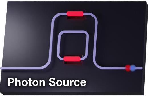
Photon sources. In order to construct entangled resource states and, in turn, an error-correcting code, photonic quantum computers consume many single photons, which must be generated with high efficiency, well-defined timing, and a high repetition rate, whilst also being spectrally pure and indistinguishable [21]. Our single-photon sources use spontaneous four-wave mixing (SFWM) [22] driven by a pulsed laser pump, where the generation of a single photon is probabilistic but heralded by the detection of its pair – making a heralded single photon source (HSPS).
The visibility of two-photon quantum interference, a key operation in photonic quantum computation, is limited by the spectral purity of the heralding single photons, which is determined by the joint spectral intensity of the photon pairs. We use resonator-based optical waveguide structures to tailor the spectral properties of the photon sources to achieve high spectral purity. The pump is aligned to a resonance frequency and single photons are generated at resonant frequencies spaced symmetrically around it, as illustrated with shaded bands in Fig. 2c. Single-ring resonator sources are intrinsically limited to a heralded photon purity of [23]. We circumvent the spectral purity limitation of single resonator sources using interferometrically-coupled resonator designs [23], which we characterized to have a measured spectral purity of without spectral filtering (Fig. 2b) [24].
Photon detection. Photonic quantum computing relies on heralding the creation of quantum states by detection of correlated photons. Examples include single photon heralding from pair sources, heralded probabilistic resource state generation, and fusion measurements. For fault-tolerance, these functions require near-unit-efficiency single-photon detection. We introduced a niobium nitride ( NbN ) layer into our photonic stack to enable high-performance manufacturable superconducting nanowire single-photon detectors (SNSPDs) [11, 12].
We use a hairpin-shaped SNSPD design [25], as depicted in Fig. 2a, with a film thickness of , nanowire width of and detector length of . When operated at temperature, these detectors exhibit clear plateaus in the photon count rate versus bias current (Fig. 2e and wafer maps in [24]), indicating high internal detection efficiency. The onchip detection efficiency is measured via cryogenic electrooptical measurements of waveguide-integrated SNSPDs [24]. Testing of screened SNSPDs yielded a median on-chip efficiency of and average value of [24], limited by the hairpin design of the detector.
Interferometers and filters. Interferometers are a key building block of integrated photonic quantum computing, enabling qubit state preparation and projection, pump filtering, switching networks, resource state generation, and fusion measurements. We use combinations of directional couplers, crossings, and rings to construct ring resonators and Mach-Zehnder-type interferometers. These components have been optimized through design-test cycles and provide predictable performance guaranteed by strict fabrication process control. An example high-contrast Mach-Zehnder interference fringe, measured with co-integrated HSPS and SNSPDs, is shown in Fig. 2d, with a extinction ratio.
Such passive circuits are reconfigurable at low frequencies using thermal phase shifters, which are commonplace in silicon photonics. While the circuit itself is cooled to cryogenic temperature (in order to support the operation of integrated superconducting single-photon detectors), the thermal phaseshifters reach local temperatures well in excess of during operation. Given the available cooling power per unit area at cryogenic temperatures, thermal insulation of the phaseshifter – using undercut regions etched from the silicon substrate (Fig. 1a,b,i) – is critical to achieve sufficient efficiency. Most if not all of these heaters are made redundant and will ultimately be removed thanks to the second-generation technologies described later in this manuscript – in particular the fabrication-tolerant source, which will not require tuning, as well as the electro-optic phaseshifter, which can operate at GHz rates.
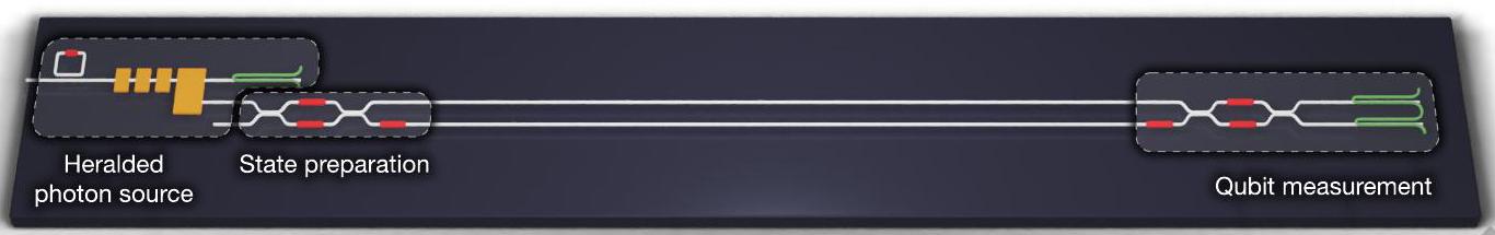
III. INTEGRATED HERALDED SINGLE PHOTON GENERATION & QUANTUM BENCHMARKING CIRCUITS
To date, photonic quantum computing platforms have depended on off-chip single photon sources, off-chip single photon detectors, or both. While sufficient for demonstration purposes, it is very challenging to achieve the heralding efficiency and component density required for practical fault tolerant quantum computing without co-integration of the source, filter and heralding detector. Through integration of our key building blocks into our semiconductor platform, we have developed the world’s first fully-integrated heralded single photon source – including source, filtering & heralding on the same chip. Using this, we construct benchmarking quantum circuits to quantify single-qubit, two-qubit and chip-to-chip qubit interconnect performance, which is summarized in Table I.
We selected photonic dies from 300 mm wafers using high-volume in-line and end-of-line electric, optical, and electro-optical room-temperature testing; as well as cryogenic
electro-optic testing for select parts. For our most complex systems, we package these dies into assemblies (Fig. 1d) together with thermal heat-sinks, more than 1000 electrical connections and up to 200 optical I/O. We house these packages in cryostats with base temperature and up to 20 W cooling capacity (Fig. 1k).
Heralded single photon source. A high performance HSPS requires engineered SFWM sources, heralding detectors, as well as a high performance filter network on-chip, which we now describe. To separate the bright laser pump from the single photons, we require suppression of the pump photons. To achieve this in an integrated circuit, we combine both interferometric in-guide filtering, and shielding of the detectors from out-of-guide scattered pump light. Inguide filtering uses a series of first-order and third-order asymmetric Mach-Zehnder interferometers combined with adddrop resonators to select single source resonances for the herald and the signal photons. Optimizing the free spectral range and coupling values of each element, we achieve pump rejection of (Fig. 2c) [24], and the simultaneous rejection of unwanted broadband parametric processes. The signal and herald photons are transmitted through filter networks with approximately 1 dB of loss. To suppress scattered light, we locally shield the detectors by encasing them in metal (Fig. 1a,b,g). The shields are constructed from deep and shallow metal-filled trenches, and back-end-of-line metals. We observe approximately 115 dB pump power suppression between the pump input and the SNSPDs.
The integrated filters and scattered light shielding, combined with co-integration of SFWMs and SNSPDs allowed for the first demonstration, to our knowledge, of successful on-chip integrated heralded single photon production, with coincidence-to-accidentals (CAR [27]) rates of up to 3000 [24].
Single qubit state preparation and measurement (SPAM). We prepare a path encoded qubit [28,29] using a heralded photon and two-mode interferometers, as illustrated in Fig. 3a. We measure the path encoded qubit using a twomode interferometer and SNSPDs. The state of the single photon in two optical modes is controlled by two thermal phase shifters, which enable the encoding of arbitrary qubit states. We observe an average single-qubit preparation and measurement fidelity of (Fig. 3e), conditional on the photon being detected [24]. Aiming to separate the impact of the HSPS’s signal to noise ratio (SNR), we repeat the measurement on a different but equivalent chip, using bright coherent light and off-chip photodetectors, achieving a fidelity of [24], showing that higher SPAM fidelity will be possible with improved HSPS SNR.
Chip-to-chip qubit interconnect. Networking of quantum modules has seen growing interest as various technologies seek to scale beyond the boundary of a single chip, trap or reticle. Telecom-wavelength photonic qubits are naturally suited for transmission through optical fiber, without the need for quantum transduction [30]. Additionally, optical fiber-based networking can enable additional novel functionality such as interleaving [31] and active-volume compilation [32] leading to large resource savings for fault-tolerant algorithms. To
demonstrate the networking capability of our photonic qubits we build a point-to-point qubit network (Fig. 3b) and assess the fidelity of qubits after propagating between modules. We prepare high-fidelity single qubit states using the same qubit state preparation circuit as described above, and convert to polarization encoding using a two-dimensional grating couplerbased path-to-polarization converter [33]. We transmit the qubit over 42 m of standard telecommunications grade optical fiber, before converting to path encoding at the receiving module and performing on-chip qubit state measurement. The transmission and receiving modules both use on-chip superconducting detectors, and operate at liquid helium temperature. We determined the Pauli transfer matrix [26] fidelity between the physical channel and the identity operation, conditional on photon arrival, to be (Fig. 3g) [24]. The system exhibits high loss associated with fiber-tochip coupling by grating couplers ( loss), which will be overcome in future systems using edge-coupled devices (discussed below).
Two-photon quantum interference. To benchmark our integrated single photon sources, we measure Hong-Ou-Mandel (HOM) quantum interference between heralded photons from two independent sources integrated on the same chip (Fig. 3c). The measured visibility depends on many factors including indistinguishability, spectral purity, number purity, signal-to-noise ratio, and system detection efficiency. To control these, we implement a single system that integrates the technologies described above: high purity, tunable photon pair sources; high extinction filter network; and high efficiency and shielded SNSPDs.
The on-chip HOM quantum interference between heralded photons from different sources, without significant spectral filtering, was (Fig. 3f), which to our knowledge is the highest measured in any platform. The experiment was performed at a pump repetition rate of 125 MHz , with a source CAR of , a heralded 0.00024 , and a maximum Klyshko efficiency of [24].
Two-qubit fusion. Bell fusion is a projective measurement onto two-qubit Bell states and is the prototypical example of the class of measurements which underpins the FBQC paradigm [13]. We implement Bell fusion using Type II fusion measurements [6] on dual rail qubits. Type II fusion uses a four mode linear optical circuit followed by photon detection. It requires both single-qubit interference and interference between qubits, enabled by high performance qubit preparations and high-visibility two-photon quantum interference, respectively.
We demonstrate that the fusion operation can perform a high fidelity projection onto a Bell state, using the benchmarking circuit in (Fig. 3d). Two independent path-encoded single qubits are prepared in the product state . Using a reconfigurable fusion-measurement network, paths are then exchanged between the qubits and the resulting state is measured via single-qubit measurements. When a photon is detected in each pair of detectors, we measure a fidelity of with the ideal Bell state. The density matrix is shown in Fig. 3h.
IV. NEXT GENERATION TECHNOLOGIES
The performance of the baseline technology described above is still not sufficient for useful photonic quantum computing. In particular, silicon waveguides incur too much propagation loss for fault tolerance, photon sources require complex and power-hungry tuning, and high-speed optical switching is unavoidably necessary to overcome the intrinsic nondeterminism of the spontaneous single photon sources.
We now describe some of the critical developments towards higher performance and additional functionality in our next-generation technology platforms, derived from multiple process flows. We focus on advanced photon sources, high-efficiency photon-number-resolving detection, low-loss waveguides, high-efficiency fiber-to-chip coupling, and onchip electro-optic phase shifters.
Cascaded resonator source. The key performance metrics for photon sources are two-photon interference visibility and photon efficiency. However, there are additional characteristics that must be addressed to enable the operation of devices at the scale of useful quantum computers. Two important considerations are the pump power required to drive the SFWM process, and the thermal-power dissipated at cryogenic temperatures to control and tune the source. We have implemented a cascaded resonator source which addresses these aspects simultaneously.
The source comprises multiple integrated resonators coupled to a single bus waveguide (Fig. 4a). Through joint optimization of the resonator-bus coupling, the resonance wavelengths, and the pump spectral amplitude, the joint spectral intensity of the source can be engineered. Our 24-resonator device has a measured upper bounded purity of [24], assuming flat spectral phase (Fig. 4b), whilst using an order of magnitude less pump power than the interferometicallycoupled source design. Even with the lower of SiN , our optimized cascaded resonator source achieves pair probability with approximately 100 pJ of pump pulse energy, which is within the range of scalable Erbium amplifiers at GHz repetition rates.
This cascaded resonators source addresses indistinguishability in a novel way. The spectrum of the photon pairs is fixed by the pump wavelength and not by the resonant wavelength of the device. Thus, global resonance shifts (e.g. from fabrication variations) have minimal impact on the spectral indistinguishability of photons generated from different devices. Fig. 4c, shows the measured indistinguishability between two sources as a function of resonance shift [24]. Using thermal tuners, we aligned two devices to the optimal operating point and applied a controlled global resonance shift to one cascaded resonator source, to simulate the impact of fabrication variation. In this implementation, we achieve two-source indistinguishability over a resonance shift window, compared to less than for a single-ring source. The built-in tolerance of the cascaded resonator source to device-to-device global wavelength variation, together with state-of-the-art fabrication control, can enable tunerless indistinguishable photon sources.
Photon-number-resolving detectors (PNRDs). The
waveguide-integrated manufacturable single-photon detectors presented earlier, while transformative, lack the photon-number-resolving capability required for FBQC. The ability to distinguish low photon numbers in detection, and to herald on that information, allows for both the removal of higherorder photon number states generated in SFWM sources, and the identification of unwanted events in fusion-based entangled state generation and computation [21].
Spatial multiplexing [34] of many SNSPD-like detector elements, as shown in Fig. 4d, can be used to assemble a scalable detector with effective photon-number resolution. In these PNRDs, the number of detected photons is approximately proportional to the amplitude of the detector output voltage. To validate this concept, we have produced waveguide-integrated PNRDs with 4 and 5 unit cells, with the best performing designs yielding on-chip detection efficiencies of (median) and (mean) (Fig. 4e) [24]. These detectors have the ability to resolve photons, as shown in the histogram of Fig. 4f [24].
Low-loss silicon nitride waveguides, directional couplers and crossings. Silicon-on-insulator waveguides are limited in waveguide propagation loss due to their large refractive index contrast [35]. Silicon nitride (SiN) waveguides, on the other hand, have lower refractive index contrast, offering a good compromise between confinement and sensitivity to manufacturing variations [35]. We have demonstrated single-mode SiN waveguide loss of and multimode waveguide loss of (Fig. 5a), measured using a cutback technique [24]. In this same platform, we have implemented waveguide crossings with loss, and waveguide splitters with loss (Fig. 5b) [24]. These component losses are away from our target value while the waveguide losses are on target.
SiN also provides advantages for photon generation. The ultra-low-loss combined with its Kerr non-linearity supports SFWM with high signal-to-noise ratio. Further, there is an absence of non-linear loss, allowing sources to operate with low loss at high-pair rates, unlike silicon, where two-photon absorption degrades performance [36].
Fiber-to-chip coupling. Low-loss coupling of light from optical fibers to our quantum photonic chips is required to make fiber networking practical. We implement novel edge coupler designs which minimize mode overlap and mode conversion loss, enabling high-performance fiber-to-chip coupling. A key challenge is to convert the highly confined onchip waveguide mode to match the much larger mode of optical fiber. To measure the insertion loss of the edge coupler, a chip is positioned between input and output optical fibers using high-precision optical alignment stages. Figure 5c shows repeated measurements from two of our best chip-tofiber coupler designs, with coupling loss to standard telecommunications grade optical fiber (SMF-28) of , and coupling loss to high-numerical aperture fiber (UHNA4) of .
Electro-optic switching. In order to overcome the intrinsic non-determinism of both spontaneous sources and fusion gates, photonic quantum computing will require beyond-state-of-the-art high-speed optical switches, in order to enable large
optical networks which can be rapidly reconfigured based on the results of previous heralded photon generation, entangling gates, and fusion outcomes [18]. The key component required for such switching networks is a high-speed, low-loss electrooptic phase shifter. Complex networks may be constructed by embedding this phase shifter into passive interferometers constructed from the beamsplitter and crossing devices previously described [18].
The performance of the phaseshifter is fundamentally constrained by the choice of electo-optic material. We incorporate barium titanate (BTO) [37] into our photonic stack as the electro-optic phase shifter. We have developed a proprietary process for the growth of high-quality BTO films using molecular beam epitaxy, compatible with foundry processes, on full 300 mm silicon wafers. We achieved a thickness uniformity of across the entire 300 mm wafer, with electrooptic Pockels values of (compared to for lithium niobate [38]), measured through free-space Pockels measurements (Fig. 5d).
The fabricated BTO Mach-Zehnder switches include a 2 mm -long phase shifter section, with a propagation loss of (Fig. 5f) and a DC of (Fig. 5g) [24]. This gives a phase shifter insertion loss of and a phase shifter half-wave loss-voltage product of , enabling a path to construction of larger low-loss switching networks required for photonic quantum computing. The insertion loss of this device is away from our target value.
V. CONCLUSION
We have described modifications made to an industrial semiconductor manufacturing process for integrated quantum photonics, demonstrating record performance. Through the addition of new materials, designs and process steps, we have enabled volume manufacturing of heralded photon sources and superconducting single photon detectors, together with photon manipulation via interferometry, tunability, and control of unwanted light. We have also described higherperforming devices, towards a resolution of the outstanding limitations of this baseline platform.
Fusion-based quantum computing supports fault-tolerant protocols which can tolerate of order total accumulated optical loss between photon emission and detection, with perqubit errors in the fusion network of order 1% [13, 39-41]. Here we have demonstrated a feature-complete set of optical components for FBQC, each with optical losses at the few-percent or below level, as well as fully integrated circuits demonstrating high-visibility interference, distribution and measurement functionalities of photonic qubits, all with sub-percent error levels.
Improvements to the platform and processes are still required. It will be necessary to further reduce SiN materials and component losses, improve filter performance, and increase detector efficiency to push overall photon loss and fidelity. Some specific examples of the remaining challenges are: implementation of low-loss fast switches towards
a multiplexed photon source; repeatable alignment and packaging of ultra-low-loss chip-to-fiber edge connects; and improved targeting and robustness of photonic designs to minimize the need for tuning and trimming with heaters, thus further reducing the heat load at cryogenic temperatures.
Finally, we note that the platforms we have developed, and their future improvements, are highly flexible. Component arrangements are highly configurable, making the system suitable for different variations of quantum computer architectures, different quantum technology applications, and indeed other photonic technologies. The ability to connect chips by fiber with very low loss makes the system technologically scalable across large numbers of photonic dies, and allows for future networking or connections between different systems in a range of application spaces. Although the singular intent of our development is a useful fault-tolerant quantum computer, we hope the impact of our industrially-manufacturable quantum photonic platform will be broad and substantial.
PsiQuantum Team.
Koen Alexander , Avishai Benyamini , Dylan Black , Damien Bonneau , Stanley Burgos , Ben Burridge , Hugo Cable , Geoff Campbell , Gabriel Catalano , Alejandro Ceballos , Chia-Ming Chang , Sourav Sen Choudhury , CJ Chung , Fariba Danesh , Tom Dauer , Michael Davis , Eric Dudley , Ping Er-Xuan , Josep Fargas , Alessandro Farsi , Colleen Fenrich , Jonathan Frazer , Masaya Fukami , Yogeeswaran Ganesan , Gary Gibson , Mercedes Gimeno-Segovia , Sebastian Goeldi , Patrick Goley , Ryan Haislmaier , Sami Halimi , Paul Hansen , Sam Hardy , Jason Horng , Matthew House , Hong Hu , Mehdi Jadidi , Vijay Jain , Henrik Johansson , Thomas Jones , Vimal Kamineni , Nicholas Kelez , Ravi Koustuban , George Kovall , Peter Krogen , Nikhil Kumar , Yong Liang , Nicholas LiCausi , Dan Llewellyn , Kimberly Lokovic , Michael Lovelady , Vitor Riseti Manfrinato , Ann Melnichuk , Gabriel Mendoza , Brad Moores , Shaunak Mukherjee , Joseph Munns , Francois-Xavier Musalem , Faraz Najafi , Jeremy L. O’Brien , J. Elliott Ortmann , Sunil Pai , Bryan Park , Hsuan-Tung Peng , Nicholas Penthorn , Brennan Peterson , Gabriel Peterson , Matt Poush , Geoff J. Pryde , Tarun Ramprasad , Gareth Ray , Angelita Viejo Rodriguez , Brian Roxworthy , Terry Rudolph , Dylan J. Saunders , Pete Shadbolt , Deesha Shah , Andrea Bahgat Shehata , Hyungki Shin , Jeffrey Sinsky , Jake Smith , Ben Sohn , Young-Ik Sohn , Gyeongho Son , Mario C. M. M. Souza , Chris Sparrow , Matteo Staffaroni , Camille Stavrakas , Vijay Sukumaran , Davide Tamborini , Mark G. Thompson , Khanh Tran , Mark Triplett , Maryann Tung , Andrzej Veitia , Alexey Vert , Mihai D. Vidrighin , Ilya Vorobeichik , Peter Weigel , Mathhew Wingert , Jamie Wooding , Xinran Zhou
Data availability: The data that support the findings in this study are available at github.com/PsiQ/2404_17570.
Acknowledgements: We thank the continual support of our investors, partners and the government agencies.
Author contributions: The platform and benchmarking experiments were conceived and planned by the PsiQuantum team. The system architecture and engineering divisions at
PsiQuantum created the data-analysis methodology, modeling, and metrological tools that powered the experiments, assembled the system, handled calibrations, and collected data. Meanwhile, the component teams were responsible for developing photonic components, and the process teams established the manufacturing platform and BTO devices. The manuscript and Supplementary Information were composed and edited by all authors.
Competing Interests: The authors declare no competing interests.
[1] J. L. O’Brien, Science 318, 1567 (2007).
[2] E. Knill, R. Laflamme, and G. J. Milburn, Nature 409, 46 (2001).
[3] T. C. Ralph, A. G. White, W. J. Munro, and G. J. Milburn, Phys. Rev. A 65, 012314 (2001).
[4] N. Yoran and B. Reznik, Phys. Rev. Lett. 91, 037903 (2003).
[5] M. A. Nielsen, Phys. Rev. Lett. 93, 040503 (2004).
[6] D. E. Browne and T. Rudolph, Phys. Rev. Lett. 95, 010501 (2005).
[7] H. Geng, Semiconductor Manufacturing Handbook. 2nd ed (New York: McGraw-Hill Education, 2018).
[8] A. G. Fowler, S. J. Devitt, and L. C. L. Hollenberg, Quantum Info. Comput. 4, 237- (2004).
[9] Y. Li, P. C. Humphreys, G. J. Mendoza, and S. C. Benjamin, Phys. Rev. X 5, 041007 (2015).
[10] T. Rudolph, APL Photonics 2, 030901 (2017).
[11] G. N. Gol’tsman, O. Okunev, G. Chulkova, A. Lipatov, A. Semenov, K. Smirnov, B. Voronov, A. Dzardanov, C. Williams, and R. Sobolewski, Applied Physics Letters 79, 705 (2001).
[12] F. Marsili, V. B. Verma, J. A. Stern, S. Harrington, A. E. Lita, T. Gerrits, I. Vayshenker, B. Baek, M. D. Shaw, R. P. Mirin, and S. W. Nam, Nature Photonics 7, 210 (2013).
[13] S. Bartolucci, P. Birchall, H. Bombín, H. Cable, C. Dawson, M. Gimeno-Segovia, E. Johnston, K. Kieling, N. Nickerson, M. Pant, F. Pastawski, T. Rudolph, and C. Sparrow, Nature Communications 14, 912 (2023).
[14] K. Giewont, K. Nummy, F. A. Anderson, J. Ayala, T. Barwicz, Y. Bian, K. K. Dezfulian, D. M. Gill, T. Houghton, S. Hu, B. Peng, M. Rakowski, S. Rauch, J. C. Rosenberg, A. Sahin, I. Stobert, and A. Stricker, IEEE Journal of Selected Topics in Quantum Electronics 25, 1 (2019).
[15] A. L. Migdall, D. Branning, and S. Castelletto, Phys. Rev. A 66, 053805 (2002).
[16] T. B. Pittman, B. C. Jacobs, and J. D. Franson, Phys. Rev. A 66, 042303 (2002).
[17] E. Meyer-Scott, C. Silberhorn, and A. Migdall, Review of Scientific Instruments 91, 041101 (2020).
[18] S. Bartolucci, P. Birchall, D. Bonneau, H. Cable, M. GimenoSegovia, K. Kieling, N. Nickerson, T. Rudolph, and C. Sparrow, (2021), arXiv:2109.13760 [quant-ph].
[19] S. Y. Siew, B. Li, F. Gao, H. Y. Zheng, W. Zhang, P. Guo, S. W. Xie, A. Song, B. Dong, L. W. Luo, C. Li, X. Luo, and G.-Q. Lo, Journal of Lightwave Technology 39, 4374 (2021).
[20] S. Shekhar, W. Bogaerts, L. Chrostowski, J. E. Bowers, M. Hochberg, R. Soref, and B. J. Shastri, Nature Communications 15, 751 (2024).
[21] S. Bartolucci, P. M. Birchall, M. Gimeno-Segovia, E. Johnston, K. Kieling, M. Pant, T. Rudolph, J. Smith, C. Sparrow, and
M. D. Vidrighin, (2021), arXiv:2106.13825 [quant-ph].
[22] J. W. Silverstone, D. Bonneau, J. L. O’Brien, and M. G. Thompson, IEEE Journal of Selected Topics in Quantum Electronics 22, 390 (2016).
[23] Z. Vernon, M. Menotti, C. C. Tison, J. A. Steidle, M. L. Fanto, P. M. Thomas, S. F. Preble, A. M. Smith, P. M. Alsing, M. Liscidini, and J. E. Sipe, Opt. Lett. 42, 3638 (2017).
[24] Supplementary Material.
[25] X. Hu, C. W. Holzwarth, D. Masciarelli, E. A. Dauler, and K. K. Berggren, IEEE Transactions on Applied Superconductivity 19, 336 (2009).
[26] J. M. Chow, J. M. Gambetta, A. D. Córcoles, S. T. Merkel, J. A. Smolin, C. Rigetti, S. Poletto, G. A. Keefe, M. B. Rothwell, J. R. Rozen, M. B. Ketchen, and M. Steffen, Phys. Rev. Lett. 109, 060501 (2012).
[27] J. C. Bienfang, J. Bienfang, T. Gerrits, P. Kuo, A. Migdall, S. Polyakov, and O. T. Slattery, IR 8486, US Department of Commerce, National Institute of Standards and Technology (2023).
[28] A. Politi, M. J. Cryan, J. G. Rarity, S. Yu, and J. L. O’Brien, Science 320, 646 (2008).
[29] J. Wang, F. Sciarrino, A. Laing, and M. G. Thompson,Nature Photonics14, 273 (2020).
[30] N. Lauk, N. Sinclair, S. Barzanjeh, J. P. Covey, M. Saffman, M. Spiropulu, and C. Simon, Quantum Science and Technology 5, 020501 (2020).
[31] H. Bombin, I. H. Kim, D. Litinski, N. Nickerson, M. Pant, F. Pastawski, S. Roberts, and T. Rudolph, (2021), arXiv:2103.08612 [quant-ph].
[32] D. Litinski and N. Nickerson, (2022), arXiv:2211.15465 [quant-ph].
[33] D. Llewellyn, Y. Ding, I. I. Faruque, S. Paesani, D. Bacco, R. Santagati, Y.-J. Qian, Y. Li, Y.-F. Xiao, M. Huber, M. Malik, G. F. Sinclair, X. Zhou, K. Rottwitt, J. L. O’Brien, J. G. Rarity, Q. Gong, L. K. Oxenlowe, J. Wang, and M. G. Thompson, Nature Physics 16, 148 (2020).
[34] S. Jahanmirinejad and A. Fiore, Opt. Express 20, 5017 (2012).
[35] W. D. Sacher, J. C. Mikkelsen, Y. Huang, J. C. Mak, Z. Yong, X. Luo, Y. Li, P. Dumais, J. Jiang, D. Goodwill, et al., Proceedings of the IEEE 106, 2232 (2018).
[36] L. M. Rosenfeld, D. A. Sulway, G. F. Sinclair, V. Anant, M. G. Thompson, J. G. Rarity, and J. W. Silverstone, Opt. Express 28, 37092 (2020).
[37] F. Eltes, G. E. Villarreal-Garcia, D. Caimi, H. Siegwart, A. A. Gentile, A. Hart, P. Stark, G. D. Marshall, M. G. Thompson, J. Barreto, J. Fompeyrine, and S. Abel, Nature Materials 19, 1164 (2020).
[38] D. Zhu, L. Shao, M. Yu, R. Cheng, B. Desiatov, C. J. Xin, Y. Hu,
J. Holzgrafe, S. Ghosh, A. Shams-Ansari, E. Puma, N. Sinclair, C. Reimer, M. Zhang, and M. Lončar, Adv. Opt. Photon. 13, 242 (2021).
[39] H. Bombin, C. Dawson, N. Nickerson, M. Pant, and J. Sullivan, (2023), arXiv:2303.16122 [quant-ph].
[40] H. Bombin, C. Dawson, T. Farrelly, Y. Liu, N. Nickerson, M. Pant, F. Pastawski, and S. Roberts, (2023), arXiv:2308.07844 [quant-ph].
[41] PsiQuantum, Manuscript in preparation.
Metric
Experiment Value (%)
Single-Qubit
SPAM fidelity
Chip-to-chip fidelity
Two-Qubit
Quantum interference visibility
Bell fidelity
TABLE I. Single- and two-qubit performance metrics. Not accounting for loss. *Second SPAM fidelity listed above is measured with bright light and off-chip detectors, see main text.
FIG. 1. Manufacturable integrated quantum photonic stack. & , Schematic of key components and process modules. We highlight (on right) additional process steps included in our next-generation platform. c, A 300 mm wafer containing single photon sources, superconducting single-photon detectors, and quantum benchmarking circuits. d, A cryogenic assembly containing a photonic die, heat-spreader, electronic PCB & 100 -channel telecom fibre attach unit. e-k, optical micrograph, scanning-electron-microscope or transmission electron microscopy images of: , photon source (top down); , optical waveguide (cross-section); , deep/shallow trench scattered light shield (cross-section); , single-photon detector (top down); , thermal-isolation trench (cross-section); , single-photon detector on waveguide (cross-section). , custom cryostat used in benchmarking experiments with cooling power at 2.2 K .
FIG. 2. Key building blocks of the platform. a, Schematics of photon source, filter network, interferometer and detector. b, Measured joint spectral intensity of an interferometrically-coupled resonator photon source, indicating a spectral purity of [24]. c, Response of our pump filter network. We shade the pump, signal and herald frequency bands and show the measured herald (orange) and signal (blue) filter spectrum, characterized with on-chip SNSPDs. d, Measured response of a Mach-Zehnder interferometer (MZI) to heralded single-photon illumination on a fully integrated platform. The extinction ratio at the transmission port is . The asymmetry in the MZI response is an artifact of a non-constant step size, which is finer around one feature only. There is no significant variation in performance across a circuit or among different circuits. e, Measured on-chip detection efficiency as a function of detector bias current ( ) normalized by the detector switching current ( ), and (inset bottom right) the detector count rate (blue) and dark count rate (orange), per second [24].
FIG. 3. Quantum Benchmarking Circuits. These circuits are reconfigurable via thermal phase shifters indicated in red in the schematics. Schematics of: a, quantum state preparation and measurement; b, point-to-point qubit network; , two-photon quantum (HOM) interference; d, two-qubit fusion measurement. e, SPAM fidelity of the reconstructed state with the target state for Pauli eigenstates. f, HOM interference. , measured Pauli transfer matrix [26] of chip-to-chip qubit interconnect channel. , reconstructed two-qubit density matrix after fusion (grey bars indicate magnitude below 0.01 threshold).
FIG. 4. Cascaded resonator source and PNRD. a, Schematic of the source. b, Measured joint spectral intensity of a cascaded resonators source showing up to purity, assuming flat spectral phase [24]. c, measured indistinguishability of two source copies as a function of the resonance wavelength offset [24]. d, Top-down optical micrograph of a SiN-waveguide-coupled PNRD, where single-photon detectors (SNSPDs) are crossing a waveguide and absorb light from the waveguide through evanescent coupling. Sets of SNSPDs are connected through on-chip resistors to comprise a unit cell. Identical unit cells are connected in series. e, On-chip detection efficiency for the PNRD shown in d as a function of normalized bias current, showing the average across 6 unique devices [24]. e-inset, distribution of single-shot detection efficiency for each of the unique devices biased at at 2 input power levels. , (left) Persistent plot of the electrical photodetection signal (voltage traces) of a 4-unit-cell PNRD. The traces were recorded using a cryogenic amplifier. The voltage traces show 5 distinct levels, corresponding to and 4 unit cells detecting photons simultaneously. (To right, voltage trace histogram).
FIG. 5. Waveguide and component loss, and BTO optical switch. a,b,c, Loss of SiN-based components with mean (black line) and median (white line). a, SiN waveguide loss measurement, showing results across example wafers for both multi-mode (MM) and singlemode (SM) waveguides [24]. b, SiN component loss for waveguide splitters and crossings [24]. c, Chip-to-fibre loss. The fiber-to-chip coupling is measured in the low-loss regime using repeated transmission measurements on two exemplary devices designed for SMF-28 fiber and an exemplary device designed for UHNA fiber [24]. d, Free-space electro-optic measurement of the effective Pockels coefficient of an MBE-grown BTO film, with hysteresis. e, Scanning electron microscope cross-section of a fully fabricated BTO-on-SiN phase shifter. f, Cutback-based propagation loss measurement of a BTO-on-SiN phase shifter (data points and guide-line), with confidence intervals provided (dashed lines). , measured optical transmission of a Mach-Zehnder interferometer (MZI) with a mm-long BTO phase shifter. A voltage was applied to one arm of the MZI, resulting in a V.cm in a non-push-pull configuration [24], where is the voltage required to change the phase by radians. Wafer maps of these results can be found in the supplementary material [24].
d.
b. Photon source
d. Mach-Zehnder Interferometer
c. Filter network
e. Superconducting nanowire single photon detector
a. Single-qubit state preparation and measurement
b. Qubit interconnect
c. Two-photon quantum interference
e. SPAM fidelity
f. Quantum interference
99.72%
g. Qubit interconnect
h. Qubit fusion measurement
a. Cascaded resonator source
b. Source JSI
c. Source-to-source indistinguishability
d. Photon number resolving detector
e. PNRD on-chip efficiency
f. PNRD readout
a. SiN waveguide loss
b. SiN component loss
d. Pockels film measurement
e. BTO phaseshifter cross-section
PsiQuantum Corp., Palo Alto 94304 CA, USA PsiQuantum Ltd., Daresbury WA4 4FS, UK